INVITED PAPER
Special Section on Recent Progress in Active Photonic Device TechnologiesMetal-Cavity Nanolasers and NanoLEDs
Shun Lien CHUANG†a), Chi-Yu NI†, Chien-Yao LU†,andAkira MATSUDAIRA†,Nonmembers
SUMMARY We present the theory and experiment of metal-cavity nanolasers and nanoLEDs flip-chip bonded to silicon under electrical in- jection at room temperature. We first review the recent progress on micro- and nanolasers. We then present the design rule and our theoretical model.
We show the experimental results of our metal-cavity surface-emitting mi- crolasers and compare with our theoretical results showing an excellent agreement. We found the important contributions of the nonradiative re- combination currents including Auger recombination, surface recombina- tion, and leakage currents. Finally, experimental demonstration of electri- cal injection nanoLEDs toward subwavelength nanoscale lasers is reported.
key words: nanolasers, nanoLEDs, microcavity, plasmonic waveguides, metal cavity
1. Introduction
There has been intensive research on subwavelength nanoscale lasers for potential applications in future gener- ation optical interconnects, optical data storage, and high resolution biochemical imaging [1]–[3]. Since the invention of the laser [4] and semiconductor lasers [5]–[8], the size of lasers has been reduced significantly. The vertical-cavity surface-emitting lasers (VCSELs) [9], microdisk lasers [10], and the photonic crystal nanolasers [11] have reduced the size of the laser toward an ultra small cavity volume al- though the physical sizes are still a few wavelengths in three dimensions. To push the size of the lasers below the diffraction limit (i.e., a size of a half wavelength in all three directions), a recent work of a naolaser with a diameter of 210 nm and a height of 1.5 mm has been realized with electrical injection at 10 K [12]. To achieve operation at room temperature, a cavity of 300 nm in width and 6 mm in length [13] has been demonstrated with pulsed operation.
A continuous wave (CW) mode laser with a similar size has also been realized [14]. A metallo-dielectric pedestal pil- lar laser with further size reduction was made with thicker optical buffer layers [15]. Optically pumped metal-cavity nano-patch lasers at 77 K [16], nano-pan lasers at 8 K [17], and nanolasers at 300 K [18] further decreased the size to subwavelength in three dimensions. Hybrid structures in- corporating photonic crystals and metals are also proposed and investigated [19], [20]. The advantages of metal-cavity nanolasers and nanoLEDs are to provide an ultrasmall cav-
Manuscript received November 30, 2011.
Manuscript revised January 27, 2012.
†The authors are with the Department of Electrical and Com- puter Engineering, the University of Illinois at Urbana-Champaign, 1406 West Green Street, Urbana, Illinois, 61801, USA.
a) E-mail: [email protected] DOI: 10.1587/transele.E95.C.1235
Fig. 1 (a) The proposed metal-cavity surface-emitting laser structure with top and bottom DBR pairs. The GaAs substrate is removed with a flip-chip bonding to the receptor (silicon) substrate. Metals (silver) are used to conformally coat the lithographically defined semiconductor structure to form a metal cavity. An active region using quantum wells is placed in be- tween carrier injection layers. The device emits light vertically through the top surface and is circular in shape. [24]–[27] (b) Proposal of a nanocoin laser structure using bulk active region surrounded by a metal cavity [30].
ity volume with low power consumption, ultrahigh speed modulation, and ultra-high density photonic integration for intrachip optical interconnect. In contrast, microdisk lasers are restricted by the diffraction limit. Although the pho- tonic crystal lasers can effectively produce a small effective modal volume, still, they require an area with a radius of several micrometers in order to have a significant quality factor. Therefore, metal-cavity nanolasers and nanoLEDs provide the potential for true reduction of cavity volume with potential high performance. The use of metals to in- crease mirror reflectivity for lasers can be traced back to the first ruby laser by Maiman [4]. Iga’s invention of VC- SEL [9] also used a 50-μm metal aperture as a reflector, while reducing the vertical size greatly. We have recently developed a fundamental formulation for nanoscale lasers taking into account the plasmonic dispersion of the metals and the negative permittivity in metal cavity structures [21]–
[23]. Metal-cavity surface-emitting microlasers have also been proposed and demonstrated experimentally [24]–[27]
showing continuous-wave (CW) operation at room temper- ature. Nanoscale LEDs with electrical injection have also been demonstrated [28], paving the way toward subwave- length nanolasers.
Our surface-emitting configuration, Fig. 1(a), for metal-cavity nanolasers [24]–[27] consists of a few inno- vations compared to other metal-cavity lasers [29]. Our Copyright c2012 The Institute of Electronics, Information and Communication Engineers
design is based on the HE11 mode of a metal-coated insulator-semiconductor (core) coaxial structure with a cir- cular beam shape, top-emitting design, which is ideal for laser sources compared to the slit or rectangular window of other nanolasers, which usually introduces optical field distortion in certain directions. For a detailed comparison of our design using the propagation mode with others such as those using a cutoff mode structure for feedback, see [29]. Our devices require the substrate removal to reduce the propagation loss of the light output through a thick sub- strate and to reduce the heating effects [26]. The complete metal encapsulation and flip-chip bonding to a silicon sub- strate improve the optical mode confinement, provide effi- cient heat removal, and most importantly, isolate individual devices from cross talk for high density photonic integra- tion. We have demonstrated CW room temperature opera- tion for both 870 nm and 995 nm lasing wavelengths micro- lasers, moving toward nanoscale lasers.
Figure 1(b) shows our proposal of a nanocoin laser for further size reduction by removing the DBR reflectors.
In this paper, we present the progress on our proposed room temperature metal-cavity surface-emitting microlasers [27] and nanoLEDs [28], which operate in continuous-wave (CW) mode with electrical injection. We also show new theoretical results based on our theoretical model and com- parison with experimental data with a very good agreement.
We identify the contributions of radiative vs. non-radiative recombination currents, such as Auger recombination, de- fect recombination, and leakage current, as a function of the injection current. We then present our conclusion and future work.
2. Theory of Nanolasers
2.1 Design Rules
To satisfy the lasing condition for a laser, the phase and the threshold conditions have to be met simultaneously. Similar to previous work [31] on our first generation metal-cavity nanolasers [24], [25], the round trip phase conditionΦ(ω)= 2mπand the net threshold modal gain conditionG(g)=0 of a transverse mode have to be satisfied [31]
Φ(ω)=φbottom DBR(ω)+φtop DBR(ω)+2NQWhQWk(QW)R +2(NQW+1)hbkR(b)+
n∈cladding
2hnkR(n) =2mπ (1) G(g)=
n∈QW s
2hnΓL,n(ω)gM,n−
n
2hnΓL,n(ω)αi,n(ω)
−ln
⎛⎜⎜⎜⎜⎜
⎜⎝ 1
|rbottom DBR(ω)|2rtop DBR(ω)2
⎞⎟⎟⎟⎟⎟
⎟⎠=0 (2) whereωis optical frequency,hQW,hb, andhnare the thick- ness of the quantum wells, the barriers, and the segments in the cladding layers, respectively.kR(QW),k(b)R , andk(n)R are the real part of the propagation constant in quantum wells, bar- riers, and cladding layers, respectively.ΓL,nis the longitudi-
Fig. 2 The layer structure, sandwiched between two DBR regions, applied to the lasing threshold condition.
Fig. 3 The standing wave pattern calculated from the FDTD method.
The field is confined in MQW’s region and decays into DBR regions.
nal optical confinement factor. NQWis the number of quan- tum wells. The schematic layer structure is shown in Fig. 2.
The resonant (lasing) wavelength is determined by the phase condition in Eq. (1). Note that the effective indices for the top DBRs are simply refractive indices of materials since there is no waveguide in that region. The threshold material gain (g) can be obtained through the threshold modal gain condition, Eq. (2), when the cavity modal gain is balanced by the sum of the intrinsic and mirror losses. Since the scat- tering loss in the interface between the pillar and substrate is ignored in Eq. (2), the calculated gain will be underesti- mated. Nevertheless, this approach gives almost the same resonant wavelength as that from the finite-difference time domain method (FDTD), and is able to show the alignment of the standing wave pattern with the quantum wells under the resonance condition. More details can be found in [31].
Once the resonant wavelength and the location of the peaks of the standing wave are found, we use FDTD to ob- tain more accurate parameters such as the quality factor,Q, wave pattern, and energy confinement factor,ΓE. We place a dipole source with the wavelength obtained from Eq. (1) at the proper position to excite HE11mode. The standing wave pattern is shown in Fig. 3.QandΓEare 1,745 and 0.021, re- spectively. Thus, the threshold material gain is 7,241 cm−1 according togth =ω/(ΓEυgQ), whereω. is the resonance frequency andυg is the group velocity [21]. The light out- put power versus injection current (L-I) curve can be solved through the rate equations, as described in Sect. 2(b) next.
2.2 Rate Equations for Nanolasers
The rate equations for a laser cavity with the presence of metal have to be dealt with carefully. Metals function as plasmas in the optical frequency regime, implying that they are lossy, dispersive, and the real part of the permittivities can become negative. The issue for modeling a metal-cavity nanolaser involves how to normalize the optical field such that the total electromagnetic energy is one photon energy [21]. The optical field normalization is needed to obtain physically meaningful spontaneous and stimulated emission rates. The energy confinement factor should be used instead of the commonly used power confinement factor since the Poynting’s vector can be negative in the plasma region when the permittivity becomes negative and dispersive [22], [23].
The rigorous rate equations used for metal cavity nanolasers are presented below:
∂n
∂t = 1 qVa
(ηiI−Il)−Rnr(n)−Rsp(n)−Rst(n)S(n) (3)
∂S
∂t =−S
τp + ΓEβspRsp(n)+ ΓERst(n)S(n) (4) where
n=carrier density (cm−3) I=injection current (A) ηi=injection efficiency q=electron charge (Coulomb) Va=active material volume (cm−3)
Rnr(n)=nonradiative recombination rate (s−1cm−3) Rsp(n)=spontaneous emission rate (s−1cm−3) Rst(n)=stimulated emission coefficient (s−1) S(n)=photon density (cm−3)
Il=leakage current (A) τp=photon life time (s)
ΓE=optical energy confinement factor βsp=spontaneous emission coupling factor
The nonradiative recombination rate accounting for the sur- face recombination and Auger recombination is:
Rnr(n)=vs
Aa
Va
n+Cn3 (5)
where
vs=surface velocity (cm/s)
Aa=the surface area of the active material (cm2) C=Auger recombination coefficient (cm6s−1).
The spontaneous emission rate coupling to the continuum modes and them-th cavity mode is
Rsp(n)=Rsp,c(n)+Rsp,m(n) (6) The first term is spontaneous emission rate coupling into the continuum modes and is defined as:
Rsp,c(n)= 1 τsp,rad
1 Va
k
fc,k(1−fv,k) (7)
where
τsp,rad=radiative life time (s)
fc,k=Fermi-Dirac occupation probability of electrons in the conduction band
fv,k=Fermi-Dirac occupation probability of electrons in the valence band.
The second term is spontaneous emission rate coupling in a specific (m-th) cavity mode and is defined as:
Rsp,m(n)=βspRsp(n)
= ΓVEaε 2π2q2
0(εR,a(ωm)+εg,a(ωm))m20ωm
dω1π(ω−ωΔωm
m)2+Δω2m (8)
×V1a
k|ˆe·pk|2πγ(Ec,k−fc,kEv,k(1−−fv,kω))2+γ2
where
εR,a=the real part of the relative permittivity in the active region
εg,a=the real part of the relative group permittivity in the active region
|ˆe·pk|=the optical momentum matrix element (kgcm/s) γ=the linewidth of optical transition (eV)
vg=the group velocity (cm/s)
Veff =the effective modal volume (cm−3) neff=the effective index of the mode.
The optical energy confinement factor should be used for dispersive media:
ΓE=
Vadrε40
εg(r, ωm)+εR(r, ωm)
|E(r)|2
Vdrε40
εg(r, ωm)+εR(r, ωm)
|E(r)|2 (9) where the relative “group permittivity,”εg(r, ωm), is
εg(r, ωm)=∂[ωεR(r, ω)]
∂ω ω=ωm (10)
andE(r) is the optical electric field atω=ωm. Finally, the stimulated emission coefficient is
Rst(n)=vgg(n) (11)
where
vg=group velocity (cm/s) g(n)=gain coefficient (cm−1)
In addition, we take into account the leakage currentIl, which can be approximated as [32]:
Il=I0exp[−(Econf,g−ΔF)/kbT] (12) whereEconf,gandΔF are the band gap energy of the elec- tron confinement layer in the active region of the laser and the separation of quasi-Fermi levels in the conduction and valence bands, respectively [32]. I0 is a fitting parame- ter. Clearly, Il is proportional to thermionic emission rate in the gain medium and it increases with carrier density, i.e.
a largerΔF, and temperature. Due to the current leakage, the carrier density is not completely pinned with increasing bias current even after the threshold condition is reached.
In addition, we use the 4×4 Luttinger-Kohn Hamilto- nian under the axial approximation [33] to calculate the op- tical gain spectra of the active region consisting of 5 pairs of In0.21Ga0.79As (4.2 nm)/Ga0.12As0.88P (6 nm) quantum wells at various carrier densities. Due to the thin barrier thickness, the wave function coupling among quantum wells occurs and this effect is taken into account in our gain model.
3. Metal Cavity Surface-Emitting Microlasers
For our metal-cavity surface-emitting microlaser [27], as illustrated in Fig. 1, optical feedback is provided by a bottom 23-pair and a top (emission side) 33-pair Al0.9Ga0.1As/Al0.12Ga0.88As quarter-wavelength DBR lay- ers. Multiple quantum wells composed of 5 pairs of In0.21Ga0.79As (4.2 nm) quantum wells and GaAs0.88P0.12
(6 nm) barriers under the strain balance condition are used in the active region. The fundamental HE11mode preserves the circular beam shape and a null-free emission pattern [27]. The round-trip phase shift is tuned to match the res- onance condition according to Eq. (1) through the introduc- tion of metal dispersion and modal characteristics into the effective index. Phase shifts from the imperfect reflection of metal/semiconductor interface are included for the reso- nance wavelength prediction. The threshold material gain gthis estimated as described in Sect. 2.
Lithography and dry etching are used to create the mi- cropost structure. A silver coating is performed by e-beam evaporation after the sidewall passivation of SiNx. The mi- cropost has a radius of∼1.0μm and a height of∼4.0μm just through the active region. A complete removal of the origi- nal GaAs substrate by wet etching and flip-chip bonding to silicon are used to transfer the devices. The etching stops right at the exposure of the DBR layers where ann-contact was deposited. In Figs. 4(a) and (b), the device shows a las- ing wavelength of 995 nm and a clear threshold of 2.6 mA in the light output power vs. injection current (L-I curve) with CW operation at room temperature. The output power goes to 8μW at a bias current of 4 mA.
Fig. 4 (a) The L-I curve under CW current injection with a threshold around 2.6 mA at room temperature. The emission power can go up to more than 8μW. (Inset: A SEM micrograph of a 2μm-diameter cavity be- fore insulator encapsulation.) (b) The corresponding spectra under different biases. A clear lasing peak at 995 nm was observed. (Inset: The cross- section electric field squared|E|2inside the active region calculated by the finite element method and the infrared camera image while operating [27].)
4. Comparison between Theory and Experiment To calculate the light output power vs. current (L-I curve) and compare it with the experimental data, the thermal ef- fect has to be considered in the rate equations. Thus, a self- consistent model has to be used, i.e., the power difference between the electrical and optical power contributes to heat dissipation and leads to increase of temperature inside the device. Therefore, leakage current, spontaneous emission and stimulated emission not only vary with carrier density but also temperature. Moreover, the high carrier density and temperature increase redshift the optical transition en- ergy due to two mechanisms: one is band gap renormaliza- tion from many-body effects and the second is the band gap change from material lattice constant change with tempera- ture.
To take these two affects into account, the reduction of energy difference for each optical transition (5 transitions due to coupling among 5 MQW’s),ΔEg, is modeled as:
ΔEg=−a(T −Tsink)−ΔEBRn˜c (13) whereT andTsink are the temperature inside the active re- gion and the temperature set in the heat sink, which is 300 K in the case, respectively, and ˜nis surface carrier density nor- malized to 1×1012cm−2. Note that the carrier density is the total carrier density within 5 quantum wells. The first term represents the effect of material band gap change with temperature and the second term is due to band gap renor- malization. a can be extracted from Hamiltonian calcula- tion. As for the band gap renormalization, it is widely be- lieved thatΔEg approximately depends on the carrier den- sity n with power of third order. However, the screening effect in InxGa1−xAs/InGaAsP latticed matched to GaAs for 980 nm laser system can alleviate the band gap shrinkage from band gap renormalization at high carrier density [34], which means that with the consideration of the screening ef- fect, the band gap shrinkage is not as significant as expected.
Based on the above discussions, we use: a=0.43 meV/K, ΔEBR=9.759 meV, and c=0.52. The dependence of elec- tron confinement layer, Al0.35Ga0.65As, on temperature [35]
is also considered in the leakage current. Figure 5 shows the comparison between theory and experiment of the L-I curve, and an excellent agreement is demonstrated.
In our calculation, the surface velocity is set as 1.01× 105cm/s,τsp,rad =2.8 ns, C=1.31×10⁻²⁹cm6/s, andηi= 0.58. The collection efficiency is used to match the theoret- ical optical output power with the experiment data.
Furthermore, the power from the spontaneous emission is also included in our theoretical L-I curve. A concave curve below the threshold current can be observed in Fig. 5.
The reason is that in the long wavelength, Auger recombina- tion can be significant and dominate in the injection current at high bias. Thus, the current is proportional ton3at high current injection. On the other hand, the light power be- low the threshold condition is from spontaneous emission, which is approximately proportional ton2. Thus, the light
Fig. 5 The comparison between theoretical L-I curve (blue dot curve) and experimental curve (red curve). The threshold current Ith is around 2.5 mA.
Fig. 6 (a) The surface recombination rate (black curve) and Auger re- combination rate (red dot curve). (b) The stimulated emission (RstS) and spontaneous emission (Rsp) rates. The former surpasses the latter at around 2.75 mA.
output power below threshold condition is proportional to current with the dependence of I2/3.
To further verify this concept, the surface and Auger recombination rates are shown in Fig. 6(a). At low current injection, the surface recombination rate is larger than the Auger recombination rate. With increase of current, Auger recombination rate dominates the nonradiative recombina- tion process and results in the concave curve below thresh- old. In addition, the stimulated emission and spontaneous emission rates are plotted in Fig. 6(b). An intentional de- tuning of 15 nm is designed in this layer structure with the consideration that the gain peak alignment with the cavity resonant wavelength at high bias.
The stimulated emission surpasses the spontaneous emission around 2.75 mA. Furthermore, the different scales
Fig. 7 The leakage current increases versus injection current. Due to increase of carrier density and temperature, leakage current increases ex- ponentially in high bias.
in Figs. 6(a) and 6(b) show the nonradiative recombination rate dominates the injection current. The surface recombi- nation rate depends on the ratio of active material area to volume, which is two over radius for cylinder, and the sur- face velocity. The large ratio of the surface area to volume is inevitable in nanolasers and thus, the reduction of sur- face velocity is necessary for decreasing threshold current.
This can be improved either by using a better passivation or making devices work at lower temperatures. To reduce the Auger recombination, one method is to use a wide band gap material or to reduce the threshold material gain, and hence, the carrier density to alleviate Auger recombination rate.
In addition, the increase of carrier density even after threshold current is clearly seen in Fig. 6(a). The clear turn- ing point after threshold current is apparent for Auger re- combination rate since it is proportional to cube ofn. The smaller slope in the Auger recombination rate after thresh- old implies the slow increase in carrier injection and the lin- earity also means Auger recombination rate dominates the current at higher bias. The reason that the carrier density is not pinned is that with increase of temperature, the quasi- Fermi distribution starts to broaden and reduces the electron and hole occupation probabilities in the transition energies.
Therefore, a larger carrier density is needed to maintain the modal gain to overcome the total loss. However, this mech- anism leads to a larger Fermi energy separation, ΔF. In conjunction with the increase of temperature, these two ef- fects enhance the increase of leakage current, which results in the rollover of the L-I curve at high bias. Figure 7 shows the trend and the leakage current increases from a negligible scale to 0.25 mA as injection current increases. According to our model, the temperature inside the laser increases from 300 K to 335 K during the operation.
The extraction of spontaneous emission coupling factor βcan be carried out from the ratio ofβRsp(n) overRsp(n);
and it obviously depends on the carrier density. Figure 8 showsβas a function of the injection current. Since both βRsp(n) andRsp(n) increase with current, there is a maxi- mum value ofβbefore threshold, which is around 0.65 mA in this case. It increases when theβRsp(n) starts to increase whileRsp(n) increases gradually. After the threshold,Rsp(n) keeps increasing due to thermal effect butβRsp(n) is saturat- ing, which makesβgradually decrease. Theβvalue around
Fig. 8 The spontaneous emission coupling factorβas a function of current. Around the threshold at 2.75 mA,βis around 0.45%.
threshold current is 0.45%. This number can be further im- proved by increasing the energy confinement factor.
5. Further Size Reduction: Metal-Cavity Surface- Emitting Nanolasers and NanoLEDs
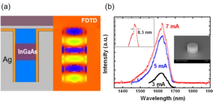
Toward nanoscale lasers with further reduction in the cavity volume, we have fabricated metal encapsulated nano-cavity light emitting diodes, which operate with electrical injec- tion at room temperature. Figure 9(a) shows a schematic diagram of our fabricated nanoLED [28], where the active region is a bulk InGaAs layer with InP cladding. The cav- ity height of this device is designed as 200 nm, leading to a fundamental HE111 mode. Figures 9(b)–(d) show SEM images of the key steps in device fabrication. The metal- defined nanocavity has a total layer thickness of 200 nm and a radius with the smallest of 750 nm. The sidewall of the disk is passivated with SiNxbefore metallization. This layer serves as a sidewall passivation, electrical isolation, and op- tical cladding layer between the active region and the sur- rounding metal. The smallest cavity volume encapsulated by silver is about 0.45μm3, which corresponds to 0.11λ30in terms of the free space wavelength.
The I-V curve, Fig. 10(a), indicates good electrical iso- lation between anode and cathode by the thin 100 nm sili- con nitride layer. It shows an excellent diode turn-on volt- age at 1.06 V. The L-I curves show a slope efficiency of 0.27 mW/A at 28◦C and 0.31 mW/A at 15◦C. The electrical injection spectra, Fig. 10(b), show no degradation compared with photoluminescence (PL) spectrum from wafer before processing, but we could not observe cavity mode or spec- trum narrowing from this device. This is because a subwave- length metal cavity suffers too large radiation loss as well as metal loss at room temperature.
In order to improve the quality factor, we have also de- signed a larger cavity metal encapsulated device in an at- tempt to fabricate a laser. The device structure is similar to Fig. 11(a) except that the height is 1.599μm, which is about six times of the previous design. This is designed such that the fundamental HE11mode has six standing wave peaks along the vertical direction (HE116). The cavity di- mension is designed in the same way as Eq. (1) with special attention on the phase shift and magnitude with the metal
Fig. 9 (a) Schematic diagram of the metal-cavity surface-emitting nanoLED. The whole InP(p)-InGaAs(i)-InP (n) is encapsulated by metal with a thin SiNxinterface layer to avoid short circuit [28]. (b) SEM de- vice picture after SiNxdeposition for isolator between anode and cathode together with sidewall passivation, (c) conformal Ag covering, and (d) fin- ished device after flip-chip bonding and substrate removal.
Fig. 10 (a) The light output and voltage vs. current curves [28], and (b) electroluminescence and photoluminescence spectra for nano-LED with ra- dius of 1.0μm (cavity volume of 0.76μm3or 0.19λ30) at room temperature.
Fig. 11 (a) The structure of the device with InGaAs as the active material and the corresponding FDTD calculation showing the electric field distri- bution inside the cavity. (b) Current-dependent spectra for a device height of 1.599μm. (c) The spectra compared with the epi-wafer photolumines- cence (PL), 200 nm height device, and 1.599μm height device, showing spectral narrowing fromΔλ=190 nm to 8.3 nm.
reflector, which is a function of the metal thickness. Fig- ure 11(a) shows the device structure and the corresponding FDTD calculation showing the electric field distribution in- side the cavity for the HE116 mode. The resonant wave- length of our numerical FDTD result agrees well with the simple Fabry-Perot design result in Sect. 2. Figure 11(b) shows the optical spectra of the metal-cavity electrical in-
jection emitters at room temperature. The cavity was fabri- cated with a radius of 1μm and a height of 1.599μm, cor- responding to a volume of 1.23λ30. Room temperature spec- trum narrowing was observed with this device. Spectral nar- rowing fromΔλ=190 nm (wafer PL spectrum) to 8.3 nm was observed with the increase of the current injection. So far, the room-temperature performance of 3D-confined sub- wavelength lasers was achieved mostly by optical pumping [16], [17] with a recent electrical injection laser at low tem- perature [15]. Our preliminary successful demonstration of a metal-encapsulated nano-cavity emitter at room tempera- ture paves the way toward the realization of electrical injec- tion nanolasers.
6. Conclusion and Future Work
In conclusion, we have presented a rigorous model and demonstrated experimentally room-temperature metal- cavity surface-emitting microlasers and nanoLEDs. Our theory explains the measured light output power vs. injec- tion current (L-I curve) of the microlasers very well and identifies the relative contributions of radiative and non- radiative (Auger and defect) recombination rates as well as leakage current. Our smaller nano-coin structures [30], shown in Fig. 1(b), exhibit LED performance as described in Sect. 5. The metal reflectors are designed to replace or integrate with the reduced number of DBR pairs based on our strategy. A pure metal mirror without the DBR can be used, provided that special care is taken with the design of its thickness. To have a good laser output power, the thickness of metal reflector should be optimized. We have demonstrated the successful coating of a thin metal layer as an output coupling mirror in the nano-LED, moving toward the realization of a nano-coin laser [30].
Nanolasers pose challenges for researchers in photon- ics, both intellectually and technologically. Due to their compactness in size and substrate-free, silicon compatibil- ity, it is promising to bridge the gap between photonics and silicon electronics. They have potential applications for ultra-high density photonic integrated circuits with ultralow power consumption and ultra-small footprint and ultrafast switching speed. The prototype of our design, with its transferability, metal-shielding, and energy efficiency, com- bined with existing technology, would bring a new appli- cation platform. The process is scalable down to subwave- length fabrication. Further research is necessary to reduce the metal losses in the cavity and to overcome the techno- logical challenges of nanofabrication.
Acknowledgments
We thank our collaborators S.W. Chang formerly at UIUC, U.S.A.; T.D. German, A. Mutig, U. Pohl, and D. Bimberg at Technical University of Berlin, Germany. We also thank L. Zhang at Bell Laboratories, Alcatel-Lucent for crystal growth of the nanoLEDepi-wafers. This work was sup- ported by DARPA NACHOS program in USA.
References
[1] R.G. Beausoleil, P.J. Kuekes, G.S. Snider, S.Y. Wang, and R.S.
Williams, “Nanoelectronic and nanophotonic interconnect,” Proc.
IEEE, vol.96, no.2, pp.230–247, Feb. 2008.
[2] D.A.B. Miller, “Device requirements for optical interconnects to sil- icon chips,” Proc. IEEE, vol.97, no.7, pp.1166–1185, July 2009.
[3] M.T. Hill, “Status and prospects for metallic and plasmonic nano- lasers,” J. Opt. Soc. Am. B, vol.27, no.11, B36-B44, 2010.
[4] T.H. Maiman, “Stimulated optical radiation in ruby,” Nature, vol.187, no.4736, pp.493–494, Aug. 1960.
[5] R.N. Hall, G.E. Fenner, J.D. Kingsley, T.J. Soltys, and R.O. Carlson,
“Coherent light emission from GaAs junctions,” Phys. Rev. Lett., vol.9, no.9, pp.366–368, Nov. 1962.
[6] M.I. Nathan, W.P. Dumke, G. Burns, F.H. Dill, Jr., and G. Lasher,
“Stimulated emission of radiation from GaAs p-n junctions,” Appl.
Phys. Lett., vol.1, no.3, pp.62–64, Nov. 1962.
[7] N. Holonyak, Jr. and S.F. Bevacqua, “Coherent (visible) light emis- sion from GaAs1−xPx junctions,” Appl. Phys. Lett., vol.1, no.2, pp.82–83, Oct. 1962.
[8] T.M. Quist, R.H. Rediker, R.J. Keyes, W.E. Krag, B. Lax, A.L.
McWhorter, and H.J. Zeiger, “Semiconductor maser of GaAs,”
Appl. Phys. Lett., vol.1, no.4, pp.91–92, Dec. 1962.
[9] H. Soda, K. Iga, C. Kitahara, and Y. Suematsu, “GaInAsP/InP sur- face emitting injection lasers,” Jpn. J. Appl. Phys., vol.18, no.6, pp.2329–2330, June 1979.
[10] A.F.J. Levi, R.E. Slusher, S.L. McCall, T. Tanbun-Ek, D.L.
Coblentz, and S.J. Pearton, “Room temperature operation of mi- crodisk laser with submilliamp threshold current,” Electron. Lett., vol.28, no.11, pp.1010–1012, May 1992.
[11] H.G. Park, S.H. Kim, S.H. Kwon, Y.G. Ju, J.K. Yang, J.H. Baek, S.B. Kim, and Y.H. Lee, “Electrically driven single-cell photonic crystal laser,” Science, vol.305, no.5089, pp.1444–1447, Sept. 2004.
[12] M.T. Hill, Y.S. Oei, B. Smalbrugge, Y. Zhu, T. de Vries, P.J. van Veldhoven, F.W.M. van Otten, T.J. Eijkemans, J.P. Turkiewicz, H. de Waardt, E.J. Geluk, S.H. Kwon, Y.H. Lee, R. Notzel, and M.K. Smit,
“Lasing in metallic-coated nanocavities,” Nature Photon., vol.1, no.10, pp.589–594, Oct. 2007.
[13] M.T. Hill, M. Marell, E.S.P. Leong, B. Smalbrugge, Y. Zhu, M.
Sun, P.J. van Veldhoven, E.J. Geluk, F. Karouta, Y. Oei, R. N¨otzel, C.Z. Ning, and M.K. Smit, “Lasing in metal-insulator-metal sub- wavelength plasmonic waveguides,” Opt. Express, vol.17, no.13, pp.11107–11112, June 2009.
[14] K. Ding, Z. Liu, L. Yin, H. Wang, R. Liu, M.T. Hill, M.J. H. Marell, P.J. van Veldhoven, R. N¨otzel, and C.Z. Ning, “Electrical injection, continuous wave operation of subwavelength-metallic-cavity lasers at 260 K,” Appl. Phys. Lett., vol.98, no.23, 231108, June 2011.
[15] J.H. Lee, M. Khajavikhan, A. Simic, Q. Gu, O. Bondarenko, B.
Slutsky, M.P. Nezhad, and Y. Fainman, “Electrically pumped sub- wavelength metallo-dielectric pedestal pillar lasers,” Opt. Express, vol.19, no.22, pp.21524–21531, Oct. 2011.
[16] K. Yu, A.M. Lakhani, and M.C. Wu, “Subwavelength metal- optic semiconductor nanopatch lasers,” Opt. Express, vol.18, no.9, pp.8790–8799, April 2010.
[17] S.H. Kwon, J.H. Kang, C. Seassal, S.K. Kim, P. Regreny, Y.H. Lee, C.M. Lieber, and H.G. Park, “Subwavelength plasmonic lasing from a semiconductor nanodisk with silver nanopan cavity,” Nano Lett., vol.10, no.9, pp.3679–3683, Aug. 2010.
[18] M.P. Nezhad, A. Simic, O. Bondarenko, B. Slutsky, A. Mizrahi, L.
Feng, V. Lomakin, and Y. Fainman, “Room-temperature subwave- length metallo-dielectric lasers,” Nat. Photon., vol.4, pp.395–399, April 2010.
[19] A.M. Lakhini, M. Kim, E.K. Lau, and M.C. Wu, “Plasmonic crystal defect laser,” Opt. Express, vol.19, no.19, pp.18237–18245, Sept.
2011.
[20] X. Yang, A. Ishikawa, X. Yin, and X. Zhang, “Hybrid photonic plas-
monic crystal nanocavities,” ACS Nano., vol.5, no.4, pp.2831–2838, March 2011.
[21] S.W. Chang and S.L. Chuang, “Fundamental formulation for plas- monic nanolasers,” IEEE J. Quantum Electron., vol.45, no.8, pp.1014–1023, Aug. 2009.
[22] S.W. Chang, T.R. Lin, and S.L. Chuang, “Theory of plasmonic Fabry-Perot nanolasers,” Opt. Express, vol.18, no.14, pp.15039–
15047, June 2010.
[23] S.W. Chang, C.Y.A. Ni, and S.L. Chuang, “Theory for bowtie plas- monic nanolasers,” Opt. Express, vol.16, no.14, pp.10580–10595, July 2008.
[24] C.Y. Lu, S.W. Chang, S.L. Chuang, T.D. Germann, and D. Bimberg,
“Metal-cavity surface-emitting microlaser at room temperature,”
Appl. Phys. Lett., vol.96, no.25, 251101, June 2010.
[25] C.Y. Lu, S.W. Chang, S.L. Chuang, T.D. Germann, U.W. Pohl, and D. Bimberg, “CW substrate-free metal-cavity surface microemit- ters at 300 K,” Semicond. Sci. Technol., vol.26, no.1, pp.014012–
014018, Nov. 2011.
[26] C.Y. Lu, S.W. Chang, S.L. Chuang, T.D. Germann, U.W. Pohl, and D. Bimberg, “Low thermal impedance of substrate-free metal cav- ity surface-emitting microlasers,” IEEE Photonics Technol. Lett., vol.23, no.15, pp.1031–1033, Aug. 2011.
[27] C.Y. Lu, S.L. Chuang, A. Mutig, and D. Bimberg, “Metal-cavity surface-emitting microlaser with hybrid metal-DBR reflectors,” Opt.
Lett., vol.36, no.13, pp.2447–2449, June 2011.
[28] A. Matsudaira, C.Y. Lu, S.L. Chuang, and L. Zhang, “Demonstra- tion of metallic nano-cavity light emitters with electrical injection,”
CLEO:2011 — Laser Applications to Photonic Applications, OSA Technical Digest (CD) (Optical Society of America, 2011), paper JMA5.
[29] M.T. Hill and M.J.H. Marell, “Surface-emitting metal nanocav- ity lasers,” Adv. Opt. Technol., vol.2011, pp.314952–314959, July 2011.
[30] C.Y. Lu and S.L. Chuang, “A surface-emitting 3D metal-nanocavity laser: Proposal and theory,” Opt. Express, vol.19, no.14, pp.13225–
13244, June 2011.
[31] S.W. Chang, C.Y. Lu, S.L. Chuang, T.D. Germann, U.W. Pohl, and D. Bimberg, “Theory of metal-cavity surface-emitting microlasers and comparison with experiment,” IEEE J. Sel. Top. Quantum Elec- tron., vol.17, no.6, pp.1681–1692, Dec. 2011.
[32] P.W. Mena, J.J. Morikuni, S.M. Kang, A.V. Harton, and K.W. Wyatt,
“A comprehensive circuit-level model of vertical-cavity surface- emitting lasers,” J. Lightwave Technol., vol.17, no.12, pp.2612 – 2632, Dec. 1999.
[33] S.L. Chuang, Physics of Photonic Devices, 2nd ed., Chapter 4, Wi- ley, New York, 2009.
[34] S.H. Park and D. Ahn, “Screening effects on the bandgap renor- malization of strained InGaAs/InGaAsP quantum well lasers lattice matched to GaAs,” Appl. Phys. Lett., vol.68, no.13, pp.1844–1846, March 1996.
[35] S.A. Lourenc¸o, I.F.L. Dias, J.L. Duarte, E. Laureto, E.A. Meneses, J.R. Leite, and I. Mazzaro, “Temperature dependence of optical tran- sitions in AlGaAs,” J. Appl. Phys., vol.89, no.11, pp.6159–6164, June 2001.
Shun Lien Chuang received the B.S. de- gree in electrical engineering from National Tai- wan University in 1976, and the M.S., E.E., and Ph.D. degrees in electrical engineering from the Massachusetts Institute of Technology in 1980, 1981, and 1983, respectively. In 1983, he joined the faculty in the Department of Electri- cal and Computer Engineering at the University of Illinois at Urbana-Champaign, where he is currently the Robert MacClinchie Distinguished Professor since 2007. He was a visitor at AT&T Bell Laboratories (1989), the SONY Research Center (1995), and NTT Basic Research Laboratories (1997). He was also a visitor at NASA Ames Research Center (1999), Fujitsu Research Laboratories (2000), Cavendish Laboratory at the University of Cambridge (2002), and Technical Univer- sity of Berlin (2009). He is conducting research on nanolasers, plasmonics, strained quantum-well and quantum-dot semiconductor lasers, and super- lattice infrared photodetectors. He is the author ofPhysics of Photonic De- vices,2nd edition, 2009, (Physics of Optoelectronic Devices, first edition, 1995), Wiley, New York. He has published more than 400 journal and con- ference papers and given many invited talks at conferences and institutions.
He served as an Associate Editor for theIEEE Journal of Quantum Elec- tronics (1997–2003)and IEEE Journal of Lightwave Technology (2007–
2008). He was a General Co-Chair for Slow and Fast Light Meeting of the Optical Society of America, July, 2008 and has served in many technical program committees of IEEE and Optical Society of America. He was a Feature Editor for a special issue inJournal of Optical Society of Amer- ica BonTerahertz Generation, Physics and Applicationsin 1994. He also edited a feature section on Mid-Infrared Quantum-Cascade Lasers in the June 2002 issue ofthe Journal of Quantum Electronics. He is a Fellow of the American Physical Society, the IEEE, and the Optical Society of Amer- ica. He has been cited many times for Excellence in Teaching at the Univer- sity of Illinois. He was selected as an Associate at the Center for Advanced Study (campus honor) at the University of Illinois in 1995. He was awarded a Fellowship from the Japan Society for the Promotion of Science to visit the University of Tokyo in 1996. He received the Engineering Excellence Award from the Optical Society of America in 2004, the IEEE Lasers and Electro-Optical Society (LEOS) Distinguished Lecturer Award for 2004–
2006, and the William Streifer Scientific Achievement Award from IEEE (LEOS) in 2007. He received the Humboldt Research Award for Senior US Scientists in 2008 and Microoptics Conference Award in 2011. He served as an elected member in the Board of Governors for the IEEE Photonics Society for 2009–2011.
Chi-Yu Ni received the B.S. degree in electrical engineering and the M.S. degree in photonics and optoelectronics from the National Taiwan University, Taipei, Taiwan, in 2000 and 2002, respectively. He is currently pursuing the Ph.D. degree in the Department of Electrical and Computer Engineering, University of Illinois at Urbana-Champaign, Urbana. His current re- search interests include semiconductor physics, mainly in optoelectronics, including plasmonic devices, lasers, and modulators.
Chien-Yao Lu received the B.S. and M.S.
degrees in electrical engineering from the Na- tional Taiwan University, Taipei, Taiwan, in 2003 and 2005, respectively. He is currently working toward the PhD degree at the Depart- ment of Electrical and Computer Engineering, University of Illinois at Urbana-Champaign, USA. He is conducting research on the design, fabrication, and characterization of nanopho- tonic and plasmonic devices. During the Ph.D.
study, he has designed and fabricated several metal-cavity lasers, including the devices used in this paper. His work on substrate-free metal-cavity microlasers won the best poster award (1st place) in international Nano-Optoelectronics Workshop (i-NOW) 2010. He was the recipient of the Nick and Katherine Holonyak, Jr. Outstanding Research Award from the Department of Electrical and Computer En- gineering, University of Illinois at Urbana-Champaign and the Bor-Uei Chen Memorial Scholarship Award from the Photonics Society of Chinese- Americans in 2011.
Akira Matsudaira received his B.S.
degree from Purdue University in 2006 and M.S. degree from University of Illinois Urbana- Champaign in 2008. He is currently pursuing his Ph.D. degree under the supervision of Pro- fessor S.L. Chuang in the Department of Electri- cal and Computer Engineering at the University of Illinois. His research includes designing, fab- rication and characterization of optoelectronic devices. He is especially interested in physics of slow light in semiconductor optical amplifier, high speed characterization of integrated photonic devices, and fabrication of practical metal cavity semiconductor nanolasers.