SREEP-2: SR-Equivalent Generator for Secure and Testable Scan Design
Katsuya Fujiwara
Dept. of Computer Science and Engineering Akita University
Akita, 010-8502, JAPAN [email protected]
Hideo Fujiwara
Graduate School of Information Science Nara Institute of Science and Technology
Nara, 630-0192, JAPAN [email protected]
Hideo Tamamoto
Dept. of Computer Science and Engineering Akita University
Akita, 010-8502, JAPAN [email protected]
Abstract—It is important to find an efficient design-for- testability methodology that satisfies both security and testability though there exists an inherent contradiction between security and testability for digital circuits. The authors reported a secure and testable scan design approach by using extended shift registers that are functionally equivalent but not structurally equivalent to shift registers [14], and clarified the cardinality of shift-register equivalents (SR- equivalents) to evaluate the security level [15]. In this paper, we present how to apply SR-equivalent circuits to scan design so that the modified scan designed circuits are both secure and testable. We consider how to design SR-equivalent circuits under several constraints and how to control/observe SR- equivalent circuits to guarantee easy scan-in/out operations. We also discuss how secure the modified scan designed circuits are. A program called SREEP-2 is presented to solve those problems.
Keywords—design-for-testability; scan design; shift register equivalents; security; scan-based side-channel attack.
I. INTRODUCTION
The design of secure chips demands protection of secret information, which may cause conflicts with the requirements for making the chip easily testable. While testing techniques such as scan design entail increased testability (controllability and observability) of the chip, they can also allow access to important data in a secure chip a lot easier. This makes it difficult for scan chains to be used especially in special cryptographic circuits where secret key streams are stored in internal registers, thus a problem in testing these types of circuits is imminent. However, quality of these circuits is highly in demand currently due to increase in the need of secure systems [3]. Fundamentally, the problem lies on the inherent contradiction between testability and security for digital circuits. Hence, there’s a need for an efficient solution such that both testability and security are satisfied. To solve this challenging problem, different approaches have been proposed [4-13]. All the approaches except [13] add extra hardware outside of the scan chain. Disadvantages of this are high area overhead, timing overhead or performance degradation, increased complexity of testing, and limited security for the registers part among others.
In [14], we proposed a secure and testable scan design approach by using extended shift registers that are functionally equivalent but not structurally equivalent to shift registers. The proposed approach is only to replace the
original scan register with a modified scan register that requires little area overhead and no performance overhead with respect to normal operation. To show the security level for the proposed approach, we clarified the cardinality of those classes of shift register equivalents (SR-equivalents) [15]. In this paper, we present how to apply SR-equivalent circuits to scan design so that the modified scan designed circuits are both secure and testable. We consider how to design SR-equivalent circuits under several constraints such as area overhead and how to control/observe SR-equivalent circuits in order to guarantee easy scan-in/out operations. We also discuss how secure the modified scan designed circuits are. A program called SREEP-2 is presented to solve those problems.
II. SR-EQUIVALENT CIRCUITS
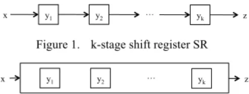
Consider a k-stage shift register shown in Figure 1. For the k-stage shift register, the input value applied to x appears at z after k clock cycles. Suppose a circuit C with a single input x, a single output z, and k flip-flops as shown in Figure 2. If the input value applied to x of C appears at the output z of C after k clock cycles, the circuit C behaves as if it is a k-stage shift register.
A circuit C with a single input x, a single output z, and k flip-flops is called functionally equivalent to a k-stage shift register (or SR-equivalent) if the input value applied to x at any time t appears at z after k clock cycles, i.e., z(t+k) = x(t) for any time t.
Figure 3 illustrates an example of 3-stage SR-equivalent circuit R1. The table in Figure 3 can be obtained easily by symbolic simulation. As shown in the table, z(3)=x(0), i.e., the input value applied to x appears at z after k=3 clock cycles, and hence the circuit is SR-equivalent. Although the input/output behavior of R1 is the same as that of the 3-stage shift register, the internal state behavior of R1 is different from the shift register. For the shift register SR, the input sequence (x(0), x(1), x(2)) which transfers SR to the state (y1(2), y2(2), y3(2)) is (x(0), x(1), x(2)) = (y3(2), y2(2), y1(2)). The initial state (y1(0), y2(0), y3(0)) can be identified as
Figure 1. k-stage shift register SR
Figure 2. k-stage SR-equivalent circuit C
y1 y2 yk
x! …! z!
x! y1 y2 …! yk z!
(y1(0), y2(0), y3(0)) = (z(2), z(1), z(0)) from the output sequence (z(0), z(1), z(2)). However, for the SR-equivalent circuit R1, the input sequence which transfers R1 to the state (y1(2), y2(2), y3(2)) is (x(0), x(1), x(2)) = (y3(2)+y2(2), y2(2), y1(2)) from Figure 3, and the initial state (y1(0), y2(0), y3(0)) can be identified as (y1(0), y2(0), y3(0)) = (z(2), z(1), z(0)+z(1)) from the output sequence. Therefore, without the information on the structure of R1 one cannot control/observe the internal state of R1. From this observation, replacing the shift register with an SR- equivalent circuit makes the scan circuit secure.
The SR-equivalent circuit shown in Figure 3 is a linear feed-forward shift register. SR-equivalent circuits can also be realized by a linear feedback shift register and/or by inserting inverters as shown in Figure 4. SR-equivalent circuits can be realized not only by linear feed- forward/feedback shift registers with/without inverters but also by more general circuits. In [15], we showed the number of k-stage SR-equivalent circuits for each type of circuits and the whole circuits. They are 2k+1-1, 2k(k+1)/2-1, 2k(k+1)/2-1, (2k(k+1)/2-1)( 2k+1-1), (2k(k+1)/2-1)( 2k+1-1), and 2k!/k!, for I2SR, LF2SR, LFSR, I2LF2SR, I2LFSR, and the whole circuits, respectively. From these cardinality of SR- equivalents, the complexity or the difficulty of identifying the structure of SR-equivalent circuits increases more than exponentially as the stage of SR increases. Hence, very high security can be realized by using SR-equivalent circuits. A. How to Design SR-Equivalent Circuits
For the class of I2SRs, any k-stage I2SR with even number of inverters is SR-equivalent. For the classes of LF2SR and I2LF2SR, any k-stage LF2SR and I2LF2SR can be modified to be SR-equivalent by manipulating the linear
sum of the output. For the classes of LFSR and I2LFSR, any k-stage LFSR and I2LFSR can be modified to be SR- equivalent by manipulating the linear sum of the input.
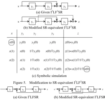
To illustrate an example, consider a k-stage I2LF2SR given in Figure 5(a). Here, k=3. By symbolic simulation illustrated in Figure 5(c), the output z(3) becomes x(2)⊕1⊕x(0). To change x(2)⊕1⊕x(0) into x(0), we add extra value x(2)⊕1 to the output z, i.e., x(2)⊕1⊕x(0)⊕x(2)⊕1=x(0). To do so, we modify the circuit by adding extra feed-forward from y1 with inverter to z as shown in Figure 5(b). Then, the modified circuit becomes SR-equivalent.
Similarly, a k-stage I2LFSR given in Figure 6(a) can be modified to the SR-equivalent circuit by adding extra feedback from y2 to x as shown in Figure 6(b).
B. How to Control/Observe SR-Equivalent Circuits
For a synthesized SR-equivalent circuits, the following two problems are important in order to utilize the SR- equivalent circuit as a scan shift register in testing. One problem is to generate an input sequence to transfer the circuit into a given desired state. This is called state- justification problem. The other problem is to determine the initial state by observing the output sequence from the state. This is called state-observation problem.
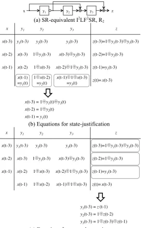
Consider a 3-stage I2LF2SR, R2, given in Figure 7(a). This I2LF2SR is SR-equivalent. Figure 7 illustrates how to solve state-justification and state-observation problem. By using symbolic simulation, we can derive equations to obtain an input sequence (x(t-3), x(t-2), x(t-1)) that transfers R2 from any state to the desired final state (y1(t), y2(t), y3(t)) as illustrated in Figure 7(b). Similarly, as illustrated in Figure 7(c), we can derive equations to determine uniquely the initial state (y1(t), y2(t), y3(t)) from the output sequence. Figure 8 illustrates the same state-justification and state- problems for another SR-equivalent I2LFSR, R3.
(a) SR-equivalent circuit R1
(b) Behavior of R1 by symbolic simulation Figure 6. Example of SR-equivalent circuit
y1 y2 y3
x! z!
x y1 y2 y3 z!
x(0) y1(0) y2(0) y3(0) z(0) = y2(0) y3(0) x(1) x(0) y1(0) y1(0) y2(0) z(1) = y2(0)
x(2) x(1) x(0) x(0) y1(0) z(2) = y1(0) x(2) x(1) x(1) x(0) z(3) = x(0)
(a) Inversion-inserted SR (I2SR) (b) Linear feed-forward SR (LF2SR)
(c) Linear feedback SR (LFSR) (d) Inversion-inserted linear feed-forward SR (I2LF2SR)
(e) Inversion-inserted linear feedback SR (I2LFSR) Figure 4. Five types of linear circuits
y1 y2 y3
x! z! x! y1 y2 y3 z!
y1 y2 y3
x! z!
y1 y2 y3
x! z!
y1 y2 y3
x! z!
(a) Given I2LF2SR
(b) Modified SR-equivalent I2LF2SR
(c) Symbolic simulation
Figure 5. Modification to SR-equivalent I2LF2SR
y1 y2 y3
x! z!
y1 y2 y3
x! z!
x y1 y2 y3 z!
x(0) y1(0) y2(0) y3(0) z(0)=y3(0) x(1) x(0) 1 y1(0) x(0) y2(0) z(1)=x(0) y2(0)
x(2) x(1) 1 x(0) x(1) 1 y1(0) z(2)=x(1) 1 y1(0)
x(2) 1 x(1) x(2) 1 x(0) z(3)=x(2) 1 x(0)
(a) Given I2LFSR (b) Modified SR-equivalent I2LFSR
Figure 3. Modification to SR-equivalent I2LFSR
y1 y2 y3
x! z! x! y1 y2 y3 z!
III. APPICATION TO SCAN DESIGN
A scan-designed circuit consists of a single or multiple scan chains and the remaining combinational logic circuit (kernel) as illustrated in Figure 9. A scan chain is regarded as a circuit consisting of a shift register with multiplexers that select the normal data from the combinational logic circuit and the shifting data from the preceding flip-flop as shown in Figure 10(a). Here, we replace the shift register with a modified SR-equivalent shift register as shown in Figure 10(b).
However, to reduce the area overhead as much as possible, not all scan chains are replaced with modified scan chains. As shown in Figure 11, only parts of scan chains necessary to be secure are replaced with modified SR- equivalent scan chains that cover secret registers to be protected, and the size of the modified scan chains is large enough to make it secure. The size of modified scan chain can be determined by the expected security level computed from the cardinality of SR-equivalent circuits that was described in the previous section. The delay overhead due to additional EOR gates influences only scan operation, and hence there is no delay overhead for normal operation.
IV. PROGRAM SREEP-2
We have considered the synthesis problem of desired SR equivalent circuits and state justification/observation problem for SR-equivalent circuits. To solve those problems,
(a) SR-equivalent I2LF2SR, R2
(b) Equations for state-justification
(c) Equations for state-observation
Figure 10. State-justification and state-observation for R2
y1 y2 y3
x! z!
x y1 y2 y3 z!
x(t-3) y1(t-3) y2(t-3) y3(t-3) z(t-3)=1 y1(t-3) y3(t-3)
x(t-2) x(t-3) 1 y1(t-3) x(t-3) y2(t-3) z(t-2)=1 y2(t-3)
x(t-1) x(t-2) 1 x(t-3) x(t-2) 1 y1(t-3) z(t-1)=y1(t-3)
x(t-1)!
=y1(t) 1=yx(t-2) 2(t) x(t-1) 1 x(t-3)
=y3(t) z(t)=x(t-3)
x(t-3) = 1 y1(t) y3(t) x(t-2) = 1 y2(t) x(t-1) = y1(t)
x y1 y2 y3 z!
x(t-3) y1(t-3) y2(t-3) y3(t-3) z(t-3)=1 y1(t-3) y3(t-3)
x(t-2) x(t-3) 1 y1(t-3) x(t-3) y2(t-3) z(t-2)=1 y2(t-3)
x(t-1) x(t-2) 1 x(t-3) x(t-2) 1 y1(t-3) z(t-1)=y1(t-3) x(t-1)! 1 x(t-2) x(t-1) 1 x(t-3) z(t)=x(t-3)
y1(t-3) = z(t-1) y2(t-3) = 1 z(t-2) y3(t-3) = 1 z(t-3) z(t-1)
(a) SR-equivalent I2LFSR, R3
(b) Equations for state-justification
(c) Equations for state-observation
Figure 9. State-justification and state-observation for R3
y1 y2 y3
x! z!
x y1 y2 y3 z!
x(t-3) y1(t-3) y2(t-3) y3(t-3) z(t-3)=1 y3(t-3)
x(t-2) x(t-3) y2(t-3) 1 y1(t-3) y3(t-3) y2(t-3) z(t-2)=1 y2(t-3) x(t-1) 1 x(t-2) y1(t-3) y3(t-3) 1 x(t-3) 1 y1(t-3) y3(t-3) z(t-1)=y1(t-3) y3(t-3)
1 x(t-1) x(t-3) = y1(t)! 1 x(t-2) = y2(t) 1 x(t-3) = y3(t) z(t)=x(t-3)
x(t-3) = 1 y3(t) x(t-2) = 1 y2(t) x(t-1) = y1(t) y3(t)
x y1 y2 y3 z!
x(t-3) y1(t-3) y2(t-3) y3(t-3) z(t-3)=1 y3(t-3)
x(t-2) x(t-3) y2(t-3) 1 y1(t-3) y3(t-3) y2(t-3) z(t-2)=1 y2(t-3) x(t-1) 1 x(t-2) y1(t-3) y3(t-3) 1 x(t-3) 1 y1(t-3) y3(t-3) z(t-1)=y1(t-3) y3(t-3)
1 x(t-1) x(t-3)! 1 x(t-2) 1 x(t-3) z(t)=x(t-3)
y1(t-3) = 1 z(t-3) z(t-1) y2(t-3) = 1 z(t-2) y3(t-3) = 1 z(t-3)
Figure 7. Scan-designed circuit
(a) Standard scan register
(b) Modified scan register (SR-equivalent) Figure 8. Standard and modified scan registers
Scan Chain!
…!
Combinational Logic Circuit (Kernel)!
Scan Chain!
…!
…!
…! …! ……! …!
y1 y2 y3
x! 0 1! z!
0 1!
0 1!
y1 y2 y3
x! 0 1! z!
0 1!
0 1!
Figure 11. Replacement of scan chain by modified scan chain
Scan Chain! Secret Register!
Secret Register!
Standard Scan Chain Modified Scan Chain Standard Scan Chain (SR-equivalent)
we made a program of SR-equivalent generator called SREEP-2 that is an updated version of our previous program SREEP (Shift Register Equivalents Enumeration and Synthesis Program) [15].
A. Synthesis for SR-Equivalent Circuits
Given several constraints, SREEP-2 generates SR- equivalent circuits that satisfy the constraints. The constraints are the number of stages or flip-flops, lower and upper limits of each number of feed-forwards, feedbacks, and inverters.
The procedure is as follows.
(1) From the given constraints, enumerate possible circuits that satisfy the constraints.
(2) For each enumerated circuit, check if it is SR- equivalent or not. If it is SR-equivalent, then it is an output as a solution. Otherwise, add extra feed- forwards, feedbacks, and/or inverters so that the modified circuit becomes SR-equivalent.
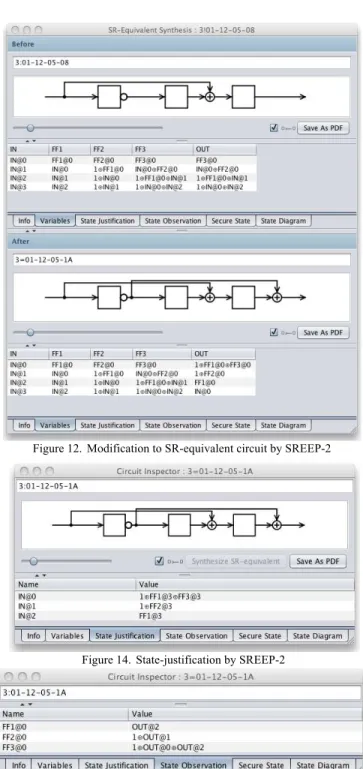
SREEP adopts GUI (graphical user interface) for expressing outcome by circuit diagram and table. SR-ID code is introduced to represent the structure of each type of linear circuit uniquely. In Appendix, some examples of the outcome by SREEP-2 are presented. Figure 12 shows an example of the outcome for step 2, modification to SR- equivalent, by SREEP-2.
B. State Justification for SR-Equivalent Circuits
Given a k-stage SR-equivalent circuit, SREEP-2 generates equations to obtain state justification sequences for the circuit. From the equations, an input sequence of length k that transfers the circuit to a desired final state can be uniquely computed.
The procedure is as follows.
(1) By symbolic simulation, express the value of each flip- flop FFi(k) at final time k by input values, x(0), x(1), …, x(k-1).
(2) Change the form of the obtained k equations into the form such that input values, x(0), x(1), … , x(k-1), are expressed by the values of flip-flops at final time k. Figure 13 shows an outcome example for state-justification by SREEP-2, which are IN@0 = 1⊕FF1@3⊕FF3@3, IN@1
= 1⊕FF2@3, and IN@2 = FF1@3. They are x(0)=1⊕FF1(3), x(1)=1⊕FF2(3), and x(2)=FF1(3). In Appendix, an outcome of state-justification for 16-bit SR- equivalent circuits is presented.
C. State Observation for SR-Equivalent Circuits
Similarly, given a k-stage SR-equivalent circuit, SREEP-2 generates equations to solve state observation problem for the circuit. From the generated equations, the initial state of the circuit can be uniquely computed from the output sequence of length k.
The procedure is as follows.
(1) By symbolic simulation, express the output values at all times, z(0), z(1), …, z(k), by the input value at time 0, x(0), and the values of flip-flops at time 0, FF1(0), FF2(0),…, FFk(0).
(2) Change the form of the obtained k equations into the form such that the value of each flip-flop, FF1(0), FF2(0),…, FFk(0), are expressed by the output values, z(0), z(1), … , z(k-1).
Figure 14 shows an outcome example for state-observation by SREEP-2, which are FF1@0 = OUT@2, FF2@0 = 1⊕OUT@1, and FF3@0 = 1⊕OUT@0⊕OUT@2. They are FF1(0)=z(2), FF2(0)=1⊕z(1), and FF3(0)=1⊕z(0)⊕z(2). D. Case study for 16-bit SR-Equivalent Circuits
The program SREEP-2 was executed on the computer with Xeon E5550 (2.66GHz x 2) with the constraints such
Figure 12. Modification to SR-equivalent circuit by SREEP-2
Figure 14. State-justification by SREEP-2
Figure 13. State-observation by SREEP-2
that the number of stages is 16, the number of feed-forwards is between 2 and 4, and the number of feedbacks is 0. The outcome of the execution is as follows. SREEP-2 took 293 seconds to generate all SR-equivalent circuits that satisfy the given constraints. The number of SR-equivalent circuits that satisfies the constraints is 58,393. Two circuits out of them are presented in Appendix. Equations to solve the state-justification and state-observation for those circuits are also presented in Appendix.
V. SECURITY LEVEL OF PROPOSED SCAN DESIGN Here, we consider how secure the modified scan designed circuits are, from two viewpoints; one is the complexity of identifying the structure of SR-equivalent circuits and the other is the possibility of leakage of the contents in each FF.
The complexity of identifying the structure of SR- equivalents is proportional to the cardinality of the class of SR-equivalents. In [15], we showed the cardinality of each class of SR-equivalent circuits. For example, the cardinality of k-stage SR-equivalent I2LF2SRs is (2k(k+1)/2-1)( 2k+1-1). Hence, the complexity or the difficulty of identifying the structure of SR-equivalent circuits increases more than exponentially as the number of flip-flops increases. So, it is very hard and intractable to identify the structure of a given SR-equivalent circuit from the information on input/output relation only.
However, even if the structure of an SR-equivalent circuit is different from that of SR and is hard to be indentified, it is not secure if part of the contents of the SR- equivalent circuit leak out. Consider the 16-bit SR- equivalent circuits C2 presented in Appendix. Suppose the size of a secret register to be protected is 8 bits. Here, if we assign 8 flip-flops from FF1 to FF8 to the secret register, the contents of the secret register appear at the output because OUT@15 = FF1@0, OUT@14 = FF2@0, OUT@13 = FF3@0, OUT@12 = FF4@0, OUT@11 = FF5@0, OUT@10 = FF6@0, OUT@9 = FF7@0, and OUT@8 = FF8@0. Hence, it is not secure. On the other hand, consider the 16-bit SR-equivalent circuits C1 presented in Appendix. The contents of all flip-flops except FF1 do not leak out. So, if we use 8 flip-flops except FF1 as the secret register, the contents of the secret register never leak out and it is secure.
To confirm the security, we need to check if the contents of each flip-flop leak out or not. SREEP-2 generates the logic expressions of the output of the circuit at each clock cycle as illustrated in Appendix, which can be used to check if the contents of each flip-flop appears at the output, i.e., it leaks out.
VI. CONCLUSION
In this paper, we presented how to apply SR-equivalent circuits to scan design so that the modified scan designed circuits are both secure and testable. We presented how to design SR-equivalent circuits under several constraints and how to control/observe SR-equivalent circuits to guarantee easy scan-in/out operations. We also considered how secure the modified scan designed circuits are, from two
viewpoints; one is the complexity of identifying the structure of SR-equivalent circuits and the other is the possibility of leakage of each FF’s contents. A program called SREEP-2 was presented to solve those problems.
ACKNOWLEDGEMENTS
This work was supported in part by Japan Society for the Promotion of Science (JSPS) under Grants-in-Aid for Scientific Research (B) (No. 20300018).
REFERENCES
[1] H. Fujiwara, Y. Nagao, T. Sasao, and K. Kinoshita, "Easily testable sequential machines with extra inputs," IEEE Trans. on Computers, Vol. C-24, No. 8, pp. 821-826, Aug. 1975.
[2] H. Fujiwara, Logic Testing and Design for Testability, The MIT Press 1985.
[3] K. Hafner, H. Ritter, T. Schwair, S. Wallstab, M. Deppermann, J. Gessner, S. Koesters, W. Moeller, and G. Sandweg, "Design and test of an integrated cryptochip," IEEE Design and Test of Computers, pp. 6-17, Dec. 1999.
[4] D. Hely, M.-L. Flottes, F. Bancel, B. Rouzeyre, and N. Berard. "Scan design and secure chip." 10th IEEE International On-Line Testing Symposium, pp. 219–224, 2004.
[5] D. Hely, F. Bancel, M.L. Flottes, and B. Rouzeyre. "Securing scan control in crypto chips." Journal of Electronic Testing - Theory and Applications, Vol. 23, No. 5, pp. 457–464, Oct. 2007.
[6] B. Yang, K. Wu, and R. Karri. "Scan based side channel attack on dedicated hardware implementations of data encryptionstandard." International Test Conference 2004, pp. 339–344, 2004.
[7] B. Yang, K. Wu, and R. Karri. "Secure scan: A design-for-test architecture for crypto chips." IEEE Trans. on Computer-Aided Design of Integrated Circuits and Systems, Vol. 25, No.10, pp. 2287–2293, Oct. 2006.
[8] J. Lee, M. Tehranipoor, and J. Plusquellic, "A low-cost solution for protecting IPs against scan-based side-channel attacks," 24th IEEE VLSI Test Symposium, pp. 94 - 99, 2006.
[9] J. Lee, M. Tehranipoor, C. Patel, and J. Plusquellic. "Securing designs against scan-based side-channel attacks." IEEE Trans. on Dependable and Secure Computing, Vol. 4, No. 4, pp. 325–336, Oct.-Dec. 2007. [10] S. Paul, R. S. Chakraborty, and S. Bhunia. "VIm-Scan: A low
overhead scan design approach for protection of secret key inscan- based secure chips." 25th IEEE VLSI Test Symposium, pp. 455–460, 2007.
[11] M. Inoue, T. Yoneda, M. Hasegawa, and H. Fujiwara, “Partial scan approach for secret information protection,” 14th IEEE European Test Symposium, pp. 143-148, May 2009.
[12] U. Chandran and D. Zhao, “SS-KTC: A high-testability low-overhead scan architecture with multi-level security integration,” 27th IEEE VLSI Test Symposium, pp. 321-326, May 2009.
[13] G. Sengar, D. Mukhopadhyay, and D. R. Chowdhury. "Secured flipped scan-chain model for crypto-architecture." IEEE Trans. on Computer-Aided Design of Integrated Circuits and Systems, Vo. 26, No.11, pp. 2080-2084, November 2007.
[14] H. Fujiwara and M.E.J. Obien, “Secure and testable scan design using extended de Brujin graph,” 15th Asia and South Pacific Design Automation Conference, pp. 413-418, Jan. 2010.
[15] K. Fujiwara, H. Fujiwara, M.E.J. Obien, and H. Tamamoto, “SREEP: Shift register equivalents enumeration and synthesis program for secure scan design,” 13th IEEE International Symposium on Design and Diagnosis of Electronic Circuits and Systems, pp. 193-196, April 2010.
[16] O. Sinanoglu and A. Orailoglu, “Modeling scan chain modifications for scan-in test power minimization,” International Test Conference 2003, pp. 602-611, 2003.
[17] SREEP: http://sreep.fujiwaralab.net/.
APPENDIX
Figure 15. C1 : 16=00001-A0002-00004-00008-00010-00020-A0041-00080-00100-00200-00400-00800-01000-02000-04100-08008-B0000
Figure 16. C2 : 16=00001-00002-00004-00008-00010-00020-00040-00080-00100-00200-00402-20800-01000-02000-04800-08040-12000