A Method of Test Generation for Path Delay Faults
in Balanced Sequential Circuits
Satoshi Ohtake
†, Shunjiro Miwa
‡and Hideo Fujiwara
††Graduate School of Information Science, Nara Institute of Science and Technology 8916-5 Takayama, Ikoma, Nara 630-0101, Japan
{ohtake, fujiwara}@is.aist-nara.ac.jp
‡Computer System LSI Division, NEC Electron Devices, NEC Corp. 1753 Shimonumabe, Nakahara-ku, Kawasaki, Kanagawa 211-8666, Japan
Abstract
This paper shows that path delay fault test generation problem for sequential circuits with balanced structure can be reduced to segment delay fault test generation problem for their combinationally transformed circuits. We also pro- pose a test generation method and a partially enhanced scan design method for path delay fault.
1. Introduction
For recent high performance VLSI circuits, delay test- ing is necessary to reach an acceptable quality level. Until now, many delay fault models are investigated[1]. Path de- lay fault model[2] is one of the most general models among them because distributed faults along paths can be tested and the delay size of detectable faults is scalable. How- ever, the path delay fault model has disadvantages that the number of faults with respect to the number of gates in a circuit is exponential in worst case and test generation for faults is generally hard. In order to avoid the former dis- advantage, a technique for selecting paths which are tar- gets of testing[3] and techniques for re-synthesizing cir- cuits such that the path count is reduced[4, 5] are proposed. The latter disadvantage can be avoided by synthesis-for- testability (SFT) techniques[1, 6] and design-for-testability (DFT) techniques[1, 7, 8].
In general, for sequential circuits, path delay fault cov- erage is low because there are many undetectable faults and time for generating delay tests is long because identi- fication of undetectable faults is time consuming problem. Chakraborty et al.[8] classified undetected faults into three categories: (A) combinationally non-activated paths, (B) se- quentially non-activated paths, and (C) unobservable fault effect. Path delay faults of the category (A) can only be
made detectable by SFT or DFT and combinational logic can be designed for path delay testability[6]. Regarding the category (B), the fault effect propagation problem is almost the same as fault effect propagation problem of stuck-at fault model. Chakraborty et al.[8] showed that almost of se- quentially undetectable faults are in the category (B). In or- der to ease complexity of test generation, sequentially unde- tectable faults must be decreased. The fully enhanced scan technique [7] and the partially enhanced scan technique [8] are proposed to achieve this claim.
Given a sequential circuit, the fully enhanced scan tech- nique replaces each FF by an enhanced scan FF. An en- hanced scan FF can store two bits to apply two consecutive vectors. For a sequential circuit designed by this technique, we can use a combinational path delay test generation al- gorithm to generate delay tests. Therefore high fault cover- age can be achieved with short test generation time. How- ever, this technique has disadvantage that hardware over- head which is caused by extra memory elements of en- hanced scan FFs is very high. This disadvantage can be avoided using partial scan techniques. In the partially en- hanced scan technique[8], for a sequential circuit, scan FFs are selected such that the feedback paths in the circuit are broken if these scan FFs are removed. For a sequential cir- cuit designed by this partial scan technique, we can consider the circuit to be a feedback free circuit during test genera- tion and test generation of the feedback free circuit is much easier than the original one. However, there is room for fa- cilitating test generation because it still requires a sequential path delay test generation algorithm.
For stuck-at fault testability of sequential circuits, in or- der to select scan FF effectively, sequential circuits are clas- sified by their structure as follows: {sequential circuits of acyclic structure} ⊃ {sequential circuit of internally bal- anced structure} ⊃ {sequential circuits of balanced struc- ture} and that internally balanced structures allow test gen-
20th IEEE VLSI Test Symposium, pp. 321-327, May 2002.
eration with combinational test generation complexity[9]. Although the number of scan FFs required to make a given sequential circuit acyclic is generally smaller than the num- ber of scan FFs required to make the circuit internally balanced[10], in order to apply a combinational test gener- ation algorithm to the acyclic sequential circuit, time frame expansion must be used[11] or multiple faults must be dealt with[10]. For a sequential circuit of balanced structure, the test generation problem of the circuit can be reduced to that of the combinationally equivalent circuit which can be ob- tained by replacing each FF in the original sequential cir- cuit by a wire. In other words, instead of using a sequen- tial test generation algorithm, tests of stuck-at faults in the sequential circuit can be obtained by generating tests for corresponding stuck-at faults in the combinationally trans- formed circuit using a combinational test generation algo- rithm. Therefore test generation time can be reduced signif- icantly [12].
In this work, we introduce this concept into path delay test generation for sequential circuits and propose a method of path delay test generation for sequential circuits of bal- anced structure. To put it concretely, in our test genera- tion method for path delay faults in a sequential circuit of balanced structure, we first make the sequential circuit into the combinationally transformed circuit. Next, we generate tests for segment delay faults[13] in the combinational cir- cuit instead of generating tests for the path delay faults in the sequential circuit. And finally, we transform the gener- ated tests for segment delay faults of the combinational cir- cuit into tests for path delay faults of the original sequential circuit. We also show reducibility between the test genera- tion problem for path delay faults of a balanced sequential circuit and that for corresponding segment delay faults of its combinationally equivalent circuit and propose a DFT method for making general sequential circuits path delay testable using enhanced scan FFs.
2. Preliminaries
2.1. Circuit ModelA sequential circuit is considered as an interconnection of combinational logic gates and FFs. The circuit is repre- sented by a directed graph defined as follows.
Definition 1 A circuit graph for a sequential circuit S is a directed graph G= (V,A,w).
• V is the set of vertices representing primary inputs, pri- mary outputs and gates in S.
• A ⊂ V ×V is the set of arcs representing FFs and wires in S.
• w : A $→ {0} ∪N(natural numbers) defines the weights of the arcs where a weight is the number of FFs be-
tween the corresponding gates. ✷
In this work, we assume that FFs have no hold capability and FFs are of D-type. This assumption does not impose restriction on circuit representation because any FF which has hold capability or is the other type can be modeled by a D-type FF and some logic gates.
2.2. Delay Fault Model
In this work, we are targeting path delay faults in sequen- tial circuits defined as follows.
Definition 2 In a sequential circuit, a path is defined as an order set of gates {g1,g2, . . . ,gn}, where g1 is a primary input or an FF and gnis a primary output or an FF. Also, gate giis an input to gate gi+1(1 ≤ i ≤ n − 1). A path has a delay fault if propagation time of rising or falling signal transition through the path exceeds a specified clock period. Such a delay fault on a path is said to be a path delay fault
(PDF)[1, 2, 8]. ✷
PDFs can be classified as follows: singly-testable (ST), multiply-testable and singly-testable dependent [14]. For each ST PDF, there exists at least one delay test that is ei- ther robust, validatable non-robust, or non-robust. These tests are identified by the off-input values of the PDF. In order to simplify the discussion, we consider generating de- lay tests for ST PDFs in a combinational part of a sequential circuit and do not distinguish conditions of off-inputs, i.e., we consider generating non-robust delay tests for ST PDFs. Definition 3 Let S and p be a sequential circuit and a path in S, respectively. Let f and Sf be a rising (falling) PDF on pand a faulty circuit of S produced by f , respectively. The fault f is testable if there exists an input sequence t for S and Sfsuch that the following conditions hold.
1. A rising (falling) signal transition is launched at the starting point (an FF or a primary input) of p of S by t. 2. The transition launched at the starting point of p is propagated to the ending point (an FF or a primary out- put) of p along p in S by t.
3. The captured or observed value induced by the transi- tion at the ending point of p of Sfis different from that of S.
4. The output sequence of S and that of Sfare different. Such an input sequence t is regarded as a PDF test se-
quence. ✷
Definition 4 In a combinational circuit, a segment is de- fined as an order set of gates{g1,g2, . . . ,gn}, where n is the length of the segment. The length of the segment, n, can be anywhere from 1 to the number of gates in the longest path in the circuit. Also, gate giis an input to gate gi+1(1 ≤ i ≤ n − 1). A segment has a delay fault if propa- gation time of rising or falling signal transition through the segment exceeds a specified limit. Such a delay fault on a segment is said to be a segment delay fault (SDF)[1, 13]. It is assumed that a segment delay fault is large enough to cause a delay fault on all paths that include the segment. ✷
Definition 5 Let C and s be a combinational circuit and a segment in C, respectively. Let f and Cfbe a rising (falling) SDF on s and a faulty circuit of C produced by f , respec- tively. The fault f is testable if there exists an input vector pair(t1,t2) for C and Cfsuch that the following conditions hold.
1. A rising (falling) signal transition is launched at the starting point (a gate or a primary input) of s of C by (t1,t2).
2. The transition launched at the starting point of s is propagated to the ending point (a gate or a primary out- put) of s along s in C by(t1,t2).
3. The value induced by the transition at the ending point of s of Cfis different from that of C.
4. The second output vector of C and that of Cf are dif- ferent.
Such an input vector pair(t1,t2) is regarded as an SDF 2-
pattern test. ✷
Notice that, it is conceivable that conditions of off-inputs of an SDF are the same as that of a PDF.
2.3. Circuit Transformation
Definition 6 Given a sequential circuit S whose circuit graph is acyclic, we define its combinational equivalent C(S) as the combinational circuit formed by replacing each FF in S by a buffer. Such a transformation is said the com- binational transformation (C-transformation). ✷ Notice that the original C-transformation [9] replaces FFs by wires. In order to clarify discussions about start- ing and ending points of SDFs, we use buffers instead of wires.
3. Balanced Structure
Our target circuit structure in our test generation method proposed in Section 4 is balanced structure. Balanced structure is defined as follows.
Definition 7 [15] A circuit graph G is defined to be a bal- anced structureif it satisfies the following conditions.
1. G is acyclic.
2. ∀(vi,vj) ∈ G all directed paths (if any) between them
have the same weight. ✷
Notice that the original definition of balanced structure [12] takes FFs which have hold capable into account. In this work, we need not consider such a FF because we assumed that such a FF was modeled by a FF of D-type with some logic gates.
Example 1 An example of a sequential circuit of balanced structure and its circuit graph are shown in Figure 1. In Figure 1 (a), from C1to C6are combinational logic blocks and from FF1to FF7are FFs.
In our test generation method, we generate delay tests for each output cone of a sequential circuit of balanced struc- ture. The circuit structure of the output cone is strongly
balanced structureas Theorem 1 below. Strongly balanced structure is defined as follows.
Definition 8 A circuit graph is defined to be a strongly bal- anced structure[15] if we can assign integer values t(vi) to its vertices such that it satisfies the condition:
t(vi) = t(vj) + w(a) ∀a(vi,vj). ✷ Example 2 An example of a sequential circuit of strongly balanced structure and its circuit graph are shown in Figure 2. In Figure 2 (b), integer values (boldfaced numbers in the figure) can be assigned to all vertices without contradiction. Theorem 1 [15] A circuit graph is a balanced structure iff it is strongly balanced with respect to each input (or output) cone.
For each output cone circuit of a sequential circuit of balanced structure, the following property is derived from Definition 1 and Theorem 1. Let tmax be the maximum value among values assigned to vertices of its circuit graph. Let Iibe a vertex, which corresponds to an input of the cone circuit, of the circuit graph. Let O be the vertex, which corresponds to the output of the cone circuit, of the circuit graph. An output value of O at tmax is only affected by an input value for Iiapplied at(tmax − t(Ii)).
4. Test Generation
In this section, we propose a new test generation method for PDFs of balanced sequential circuits.
4.1. Test Generation Method
Given a balanced sequential circuit SB, the test genera- tion method proceeds as follows.
For each output cone circuit SBc of SB, 1. Make a PDF list F of SBc.
2. Transform SBc into the combinationally equivalent cir- cuit C(SBc) by C-transformation.
3. Transform F into a SDF list FCof C(SBc). 4. Generate a 2-pattern test set TCfor FCof C(SBc). 5. Transform TCinto a delay test set T for F of SBc. Notice that, if SBis of strongly balanced structure, we can apply the above procedure for the whole circuit SBwithout considering cone circuits of SB.
Here, we define the fault transformation from F into FC in step 3 of the above procedure as follows.
Definition 9 Let p be a path in SB. Let gs and ge be the starting point and the ending point of p, respectively. Let s be a segment in C(SB) such that the starting point is a primary input or a buffer corresponding to gsand the ending point is a primary output or a buffer corresponding to ge. Let fpand fsbe a rising (resp. falling) PDF on p and a rising (resp. falling) SDF on s, respectively. A transformation ϕ from fpof SBinto fs(= ϕ( fp)) of C(SB) is called the fault
transformation. ✷
C1 C3 C5
C2 C4 C6
I1
I2
I3
O1
O2
FF2
FF1
FF3
FF5
FF4
FF7
FF6
(a) (b)
0 0
0 0
0
2
1 1
1 1
1
Figure 1. Balanced sequential circuit (a) and its circuit graph (b).
C1 C3 C4
C2 C5
I1
I2
I3
O1
O2
FF2
FF1
FF4
FF3
FF6
FF5
(a) (b)
0 0
0 0
0
2 1
1 1
1
2 2
1 0
1 2
2 1
0 1
Figure 2. Strongly balanced sequential circuit (a) and its circuit graph (b).
It is obvious that any PDF in SBcan be transformed into an SDF in C(SB) by the fault transformation. There exists a one-to-one mapping from a PDF in SBto an SDF in C(SB). The delay tests transformation in step 5 is defined as se- quence transformationin the next subsection.
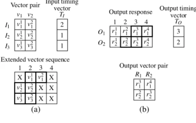
4.2. Reducibility of Test Generation Problems Given an balanced sequential circuit SB, our task of PDF test generation is to generate delay tests for all the testable PDFs. To prove the test generation method can generate delay tests for all the testable PDFs, we show that test gen- eration problem1for a set of all the PDFs FBin SBcan be reduced to that for a set of SDFs FCB in C(SB) where an SDF is transformed from a PDF by the fault transformation. We first consider strongly balanced sequential circuits. Let G be a circuit graph of a strongly balanced sequen- tial circuit SSB. Let t(qi) be an integer value which can be assigned to a vertex qisuch that it satisfies the condi- tion of Definition 8. Let tmax and tmin be the maximum value and the minimum value among values assigned to vertices of G, respectively. Let Ij( j = 1,2, . . . ,n) be a ver- tex, which corresponds to an input of SSB, of G. A vec- tor TI = (α1,α2, . . . ,αn) such that αj= tmax − t(Ij) + 1 is said to be an input timing vector of SSB. For exam- ple, an input timing vector of the circuit of Figure 2 is TI= (2,1,1) whose coordinates correspond to the primary inputs(I1,I2,I3).
Let L be tmax − tmin + 2. Let (v1,v2) be an n-bit vector pair where a vector vl is(vl1,v2l, . . . ,vlj, . . . ,vln). A vector
1A test generation problem for a fault set of a circuit consists of both generating tests for all the testable faults in the fault set and to identify untestable faults in the fault set.
X
v13 v12
v11
v23 v22
v21
X X
X
X X
r11 r12
r12 r22
r31 r32
r41 r42 v11
v13 v12
v21
v23 v22 v1 v2
1 2 3 4
1 2 3 4
Vector pair
Extended vector sequence
Output response
r31 r22
r14 r23 R1 R2 Output vector pair I1
I3 I2
2
1 1 TI
3 2 TO O1
O2 Input timing
vector Output timing
vector
(a) (b)
Figure 3. Extended vector sequence (a) and output vector pair (b)
sequence[xi j] of length L such that
xi j=
v1j if i= αj
v2j if i= αj+ 1 don’t care otherwise
is said to be an extended vector sequence of(v1,v2) with respect to TI. A transformation M which transforms from (v1,v2) into the extended vector sequence with respect to TI
is referred to as sequence transformation with respect to TI. For example, in Figure 3(a), a vector pair for the circuit of Figure 2 is transformed into the extended vector sequence with respect to the input timing vector TI.
Let Ok(k = 1,2, . . . ,m) be an vertex, which corresponds to an output of SSB, of G. A vector TO= (β1,β2, . . . ,βm) such that βk= tmax − t(Ok) + 1 is said to be an output tim- ing vectorof SSB. For example, an output timing vector of the circuit of Figure 2 is TO= (3,2) whose coordinates cor-
respond to the primary outputs(O1,O2).
Let R(C(SSB)) be an output vector pair of C(SSB) when an n-bit vector pair (v1,v2) is applied to C(SSB). Let r(Ok,βk) be an output response of a primary output corresponding to Ok at time βk when the extended se- quence of the vector pair (v1,v2) with respect to TI is applied to SSB. Let R(SSB) be a vector pair such that R(SSB) = ((r(O1,β1),r(O2,β2), . . . ,r(Om,βm)),(r(O1,β1+ 1),r(O2,β2+ 1), . . . ,r(Om,βm+ 1))). Such a vector pair R(SSB) is referred to as an output vector pair with respect to TOof SSB. For example, consider again the circuit of Figure 2, an output vector pair with respect to the output timing vector TOis obtained from an output sequence as shown in Figure 3(b).
For the relation between R(C(SSB)) and R(SSB), we can have the following lemma.
Lemma 1 The response R(C(SSB)) of C(SSB) for any n-bit vector pair and the response R(SSB) of SSBfor the extended sequence of the vector pair with respect to TI of SSB are identical.
For testable PDF of SSB, we can have the following lemma.
Lemma 2 For any testable PDF of SSB, there exists a test sequence formed as an extended sequence with respect to TI.
We call such a test sequence formed as an extended se- quence a 2-pattern extended test sequence.
The proofs of Lemma 1 and Lemma 2 are omitted here due to limitations of space. However, Lemma 1 can be eas- ily proved from Definition 8 and Lemma 2 can be easily proved from Definition 8 and Definition 3.
Let FSBbe the set of all the PDFs of SSB. Let FCSBbe a set of SDFs of C(SSB), where an SDF is transformed from a PDF by the fault transformation ϕ.
Theorem 2 The test generation problem for FSB of SSB can be reduced to the test generation problem for FCSBof C(SSB).
Proof: There exists a one-to-one mapping ϕ from a PDF in SBto an SDF in C(SB). We show that (i) a PDF fp∈ FSB
of SSBis testable iff ϕ( fp) ∈ FCSBof C(SSB) is testable and (ii) there exist a delay test transformation which transforms from a delay test for ϕ( fp) of C(SSB) into a delay test for fp
of SSB.
(i) Sufficiency: We show that if fp∈ FSBis testable, fs= ϕ( fp) ∈ FCSBis also testable. Let SSBf and C(SSBf ) be faulty circuits of SSB produced by fp and of C(SSB) produced by fs, respectively. We divide SSBf and C(SSBf ) into faulty parts and fault free parts and consider these faulty and fault free parts individually.
Faulty parts: Let C be a maximum region of connected combinational subcircuit in SSBf such that its inputs are ei- ther primary inputs or outputs of FFs, its outputs are ei- ther primary outputs or inputs of FFs, and it has the starting
point of fp as an input and the ending point of fp as an output. From Lemma 2, there exists a 2-pattern extended test sequence tpif fpis testable. From Definition 3, if fp is testable, tpmust justify a 2-pattern test(vC1,vC2) for fpof Cto the inputs of C from primary inputs of SSB and must propagate an error appeared at an output corresponding to the ending point of fpof C to a primary output of SSB. Let C′be a subcircuit corresponding to C in C(SSBf ). Circuits C and C′are the same faulty circuits and fpof C and fsof C′ can be considered as PDFs of combinational circuits C and C′. Therefore if fp is testable by(vC1,vC2) in C, fsis also
testable by(vC1,vC2) in C′.
Fault free parts: Consider a circuit SSB′produced from SSBf by replacing C with primary inputs and primary outputs and a circuit C(SSB′) produced from C(SSBf ) by replacing C′with primary inputs and primary outputs. Let G′be the circuit graph of SSB′ and its each vertex has the same in- teger value of the corresponding vertex of G. Let TI′ and TO′ be the input timing vector and the output timing vec- tor of SSB′, respectively. Let tp′ be an extended sequence of a vector pair with respect to TI′. Let M′and M′−1be an sequence transformation with respect to TI′and its inverse transformation, respectively. Let R(C(SSB′)) be the output vector pair when M′−1(t′p) is applied to C(SSB′). Let R(SSB′) be the output vector pair with respect to TO′ when t′pis ap- plied to SSB′. From Lemma 1, R(SSB′) and R(C(SSB′)) are identical because SSB′and C(SSB′) are a fault free strongly balanced circuit and its combinationally equivalent circuit, respectively. Therefore, if(vC1,vC2) can be justified to the in- puts of C in SSBf when tpis applied to the primary inputs of SSB,(vC1,vC2) must be justified to the inputs C′in C(SSBf ) by applying M−1(tp) to the primary inputs of C(SSBf ), where M−1is the inverse transformation of M. Furthermore, if the error appeared at the output of C affects a primary output of SSBf when tpis applied to SSBf , the error appeared at the output of C′must affects a primary output of C(SSBf ) when M−1(tp) is applied to C(SSBf ). Thus, if the responses of SSB and SSBf when tp is applied are different, the responses of C(SSB) and C(SSBf ) when M−1(tp) is applied are different.
Hence, if fp is testable by tp, fs is also testable by M−1(tp).
Necessity: We show that if fs∈ FCSBis testable, fp= ϕ−1( fs) ∈ FSBis also testable as the same way as the proof of sufficiency.
Faulty parts: Consider again faulty subcircuit C′and C. From Definition 5, if fs is testable in C′, there exists a 2- pattern test(vC′1 ,vC′2) for fs of C′. C′ and C are the same faulty circuits and fs and fp are the same PDFs of these circuits. Therefore if fsis testable by(vC′1,vC′2) in C′, fpis also testable by(vC′1,vC′2) in C.
Fault free parts: Consider again the circuits C(SSB′)
and SSB′. Let ts′ be an input vector pair of C(SSB′). Let R′(C(SSB′)) be the output vector pair when ts′is applied to C(SSB′). Let R′(SSB′) be the output vector pair with re- spect to TO′ when M(ts′) is applied to SSB′. From Lemma 1, R′(C(SSB′)) and R′(SSB′) are identical because SSB′ and C(SSB′) are a fault free strongly balanced circuit and its combinationally equivalent circuit, respectively. Therefore, if (vC′1,vC′2) can be justified to the inputs of C′ in C(SSBf ) when a 2-pattern test tsis applied to the primary inputs of C(SSB), (vC′1,vC′2) must be justified to the inputs C in SSBf by applying M(ts) to the primary inputs of SSBf . Furthermore, if the error appeared at the output of C′ affects a primary output of C(SSBf ) when tsis applied to C(SSBf ), the error ap- peared at the output of C must affects a primary output of SSBf when M(ts) is applied to SSBf . Thus, if the responses of C(SSB) and C(SSBf ) when tsis applied are different, the re- sponses of SSBand SSBf when M(ts) is applied are different. Hence, if fsis testable by ts, fpis also testable by M(ts). (ii) From (i), any 2-pattern test tsfor fs= ϕ( fp) ∈ FCSB can be transformed into a delay test M(ts) for fp∈ FSB. Therefore, there exists a delay test transformation M such that M transforms from a delay test for ϕ( fp) of C(SSB) into
a delay test for fpof SSB. ✷
Next, we expand Theorem 2 into balanced sequential cir- cuits.
Theorem 3 The test generation problem for FBof SB can be reduced to the test generation problem for FCBof C(SB). Proof: From Theorem 1, the output cone circuit SBc of each primary output of SBis strongly balanced. From Theorem 2 the test generation problem for PDFs of SBc can be reduced to the test generation problem for corresponding SDFs of C(SBc). The generated delay tests of SBc can be applied to SB because the primary inputs of SBexcept for the primary in- puts of SBc do not affect the primary output of SBc. Therefore
the theorem holds. ✷
4.3. Complexity of Reduction
For stuck-at fault model, the class of balanced sequential circuits has combinational test generation complexity[9]. For PDF model, we reduce test generation problem for a PDF fpof a balanced sequential circuit S to test generation problem for an SDF fsof its combinationally equivalent cir- cuit C. Here, we briefly discuss (i) the time complexities of sequential PDF test generation and combinational SDF test generation, (ii) the time complexity of C-transformation, (iii) the sizes of circuits S and C, and (iv) the sizes of faults
fpand fs.
(i) It is conceivable that the time complexity of combina- tional SDF test generation is much smaller than that of se- quential PDF test generation.
(ii) It is obvious that the time complexity of C- transformation is much smaller than the time complexity of
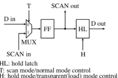
FF HL
MUX
D in D out
SCAN out
SCAN in T
0 1
H HL: hold latch
T: scan mode/normal mode control H: hold mode/transparent(load) mode control
Figure 4. Enhanced scan FF.
combinational SDF test generation.
(iii) The numbers of gates of S and C are the same. (iv) The numbers of gates on a path corresponding to fpand on a segment corresponding to fsare the same.
Therefore, we can say that the class of balanced sequential circuits has combinational path delay test generation com- plexity.
5. DFT for PDF testability
5.1. Partially Enhanced Scan DesignIn order to apply the proposed test generation method to general sequential circuits, we use partial scan technique. For a PDF of a path in a sequential circuit, a transition must be launched at the starting point of the path by the system clock. Therefore each scan FF must store at least two bits. Such a scan FF is referred as an enhanced scan FF (ESFF) [7]. An example of such an ESFF is shown in Figure 4. The ESFF is composed of a standard scan FF and an extra hold latch (HL).
Our partially enhanced scan method for a given sequen- tial circuit consists of the following two steps.
1. Select FFs of the circuit such that the circuit becomes balanced structure if these FFs are removed.
2. Replace each FF selected at the first step by an ESFF. The first step is done by the Balancing Procedure of [12] or the Balancing Algorithm of [10]. The second step is just replacing FFs by ESFFs and making a scan chain. The number of scan FFs of this partially enhanced scan method for PDFs is the same as that of the methods of [12] and [10]. The extra hardware overhead of this partially en- hanced scan method is n×Area(HL) compared with these methods where n is the number of ESFFs and Area(HL) is the area of an extra hold latch. The area overhead of our partially enhanced scan method is smaller compared to fully enhanced scan method [7]. The test generation complexity of our partially enhanced scan method is smaller than the partially enhanced scan method based on acyclic structure [8] in return for paying larger hardware compared to the partially enhanced scan method [8].
5.2. Application of Delay Test
Given a circuit S designed by our partially enhanced scan method, the test plan for applying a 2-pattern extended test sequence tpfor a PDF f is as follows. N is the number of ESFFs in S, L is the length of tpand t-th clock is operational speed clock to propagate transition through f . Each don’t care value of tpcan be replaced by either 0 or 1.
For application of tp, the t-th vector of tp must be ap- plied at operational speed after the(t − 1)-th vector of tpis
applied. Therefore, the(t − 1)-th vector and the t-th vector must be applied as follows. First, we scan in the(t − 1)- th vector using scan mode for N scan clock cycles. Second, we transfer each value of the(t −1)-th vector to each HL by placing HLs in the load mode and then place HLs in the hold mode. Next, we scan in the t-th vector using scan mode for Nscan clock cycles. Finally, we apply an operational speed clock for all the FFs using normal mode with placing HLs in the load mode. The other vectors of tpcan be applied as the above scheme or traditional scan scheme with placing HLs in the load mode. Notice that, in order to assume S is fault free circuits during application of vectors of tpexcept for the t-th and the(t − 1)-th vectors, low speed clocks must be applied to all the FFs in stead of system clock. During scan clocks are applied to ESFF, we must disable system clock for normal FFs (i.e., place normal FFs in the hold mode).
For observation of the response of tp, it is sufficient that at least one error can be observed. If an error are propa- gated to a primary output, the error can be observe from the primary output. If an error are captured at an ESFF, the er- ror can be scanned out and can be observed from the scan output of the circuit.
Consider reduction of test application time. Since each delay test for PDFs of S has many don’t care values, it is conceivable that compaction techniques are useful for re- ducing test application time. The problem of test applica- tion time reduction is our future work.
6. Conclusion
In this paper, we proposed a method of path delay test generation for sequential circuits of balanced structure and showed the correctness of the method. We also proposed a DFT method for making general sequential circuits path de- lay testable using enhanced scan FFs. It is conceivable that the test generation time and fault coverage can be improved by the methods.
Future works are to evaluate effectiveness of the method by experiments using benchmark circuits and to reduce test application time.
Acknowledgments This work is supported in part by Japan Society for the Promotion of Science (JSPS) under the Grant-in-Aid for Scientific Research A (No.12780226)
and by Foundation of Nara Institute of Science and Tech- nology under the Grant for Activity of Education and Re- search.
References
[1] A. Krstic and K.-T. T. Cheng: Delay fault testing for VLSI circuits, Kluwer Academic Publishers, 1998.
[2] G. L. Smith: “Model for delay faults based upon paths,” in Proc. of Int. Test Conf., pp. 342–349, 1985.
[3] K. Heragu, V. D. Agrawal and M. L.Bushnell: “Statistical methods for delay fault coverage analysis,” in Proc. of VLSI Design, pp. 166–170, 1995.
[4] A. Krstic and K.-T. T. Cheng: “Resynthesis of combina- tional circuits for path count reduction and for path de- lay fault testability,” in Proc. of European Design and Test Conf., pp. 486–490, 1996.
[5] I. Pomeranz and S. M. Reddy: “On synthesis-for testabil- ity of combinational logic circuits,” in Proc. of 32nd Design Automation Conf., pp. 126–132, 1995.
[6] A. K. Pramanick and S. M. Reddy: “On the design of path delay fault testable combinational circuits,” in Proc. of 20th Fault Tolerant Computing Symp., pp. 374–381, 1990. [7] B. I. Dervisoglu and G. E. Strong: “Design for testability:
Using scanpath techniques for path-delay test and measure- ment,” in Proc. of Int. Test Conf., pp. 365–374, 1991. [8] T. J. Chakraborty, V. D. Agrawal and M. L. Bushnell: “De-
sign for testability for path delay faults in sequential cir- cuits,” in Proc. of Design Automation Conf., pp. 453–457, 1993.
[9] H. Fujiwara: “A new class of sequential circuits with com- binational test generation complexity,” IEEE trans. on Com- puter, Vol. 49, No. 9, pp. 895–905, Sep. 2000.
[10] Y. C. Kim, V. D. Agrawal and K. K. Saluja: “Combinational test generation for various classes of acyclic sequential cir- cuits,” in Proc. of Int. Test Conf., pp. 1078–1087, 2001. [11] T. Inoue, T. Hosokawa, T. Mihara and H. Fujiwara: “An op-
timal time expansion model based on combinational ATPG for RT level circuits,” in Proc. of Asian Test Symp., pp. 190– 197, 1998.
[12] R. Gupta, P. Gupta and M. A. Breuer: “The BALLAST methodology for structured partial scan design,” IEEE trans. on Computer, Vol. 39, No. 4, pp. 538–544, Apr. 1990. [13] K. Heragu, J. H. Patel and V. D.Agrawal: “Segment delay
faults: A new fault model,” in Proc. of VLSI Test Symp., pp. 32–39, 1996.
[14] M. A. Gharaybeh, M. L. Bushnell and V. D. Agrawal: “Clas- sification and test generation for path-delay faults using sin- gle stuck-at fault tests,” Journal of Electronic Testing: The- ory and Applications, Vol. 11, pp. 55–67, 1997.
[15] A. Balakrishnan and S. T. Chakradhar: “Sequential circuits with combinational test generation complexity,” in Proc. of VLSI Design, pp. 111–117, 1996.