D&T
ira nsia:n o_n
This article is translated in revised form from
Monographs
of
theDes4itn
Awtoiatnior
Working Grouip oftheInform,ation ProcessingSocietv ofJapan, Vol. 19,No.3, Nov. 1983. and isreprinted withpermission. © 1983 IPS.1
Design for Testability
for Complete Test
Coverage
Very large scale circuits present great obstacles to complete
testing. A pattern generation algorithm offers a direct approach
to the problem.
Akira Motohara and Hideo Fujiwara, Osaka University
T he
problem
ofreliability
isgain- make
itdifficult
toachieveahigh
rateT
ing increasing importance with of test coverage.the rapid advance of semiconductor
Designing
fortestability
has been technology toward very large scale in- offered as asolution of
thisproblem
tegration of logic circuits. The very (see Williams and Parkeri).
Methods large scale of the circuits, however, to reduce thecomplexity
oftesting
for makes test pattern generationextreme-sequential circuits
to thelevel for
com-ly difficult,
and when test patterns can-binational circuits
havebeen proposed
not be obtained within the allowed andachieved.24 However, for
com- computation time, abortedfaults
binationalcircuits of large scale,
it is stillextremely
difficultto achieve 100 percent test coverage.summary Among the
mostpromising DFT
Some design-for-testability techniques, such as level-sensitive scan methods are those aimed at complete design, scan path, and scan/set, reduce test pattern generation of sequen- test coverage through the addition ofa tial circuits to that ofcombinational circuits by enhancing the controllabili- few hardware elements to thecircuit. ty and/or observability of all the memory elements. However, even for
com-
This redundant hardware is called test binational circuits, 100 percent test coverage of large-scale circuits ispoints. 5'6
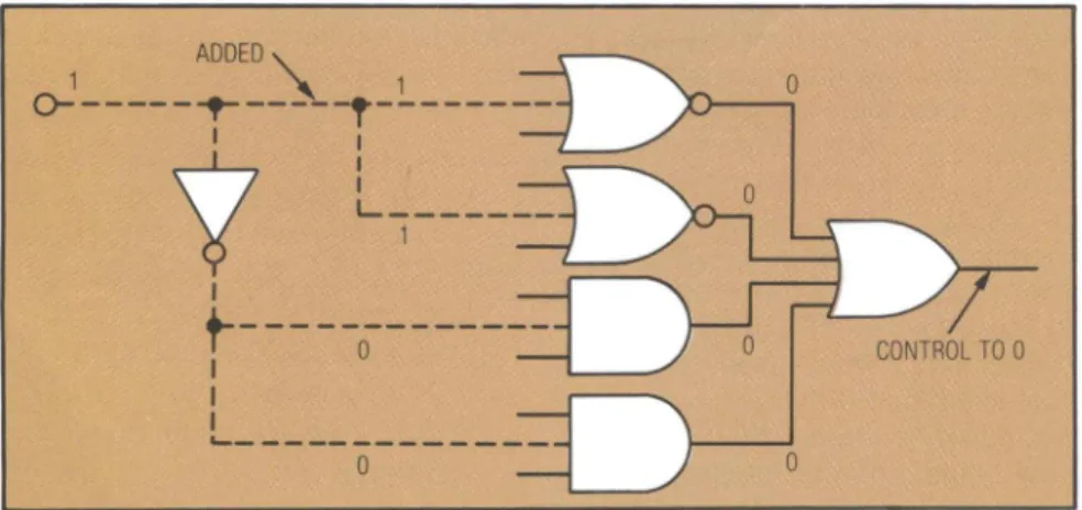
The test point strategies we generally very difficult to achieve. This article presents DFT methods are considering here fall into four cate- aimedatachievingtotalcoverage. Two methods arecompared: One,basedgories-
on testability analysis, involves the addition of test points to improve
g1
Iert
AND OR t testability beforetest pattemgeneration.The other method employs a test(1) Inse N,O gates.
pattem generation algorithm(the FAN algorithm). Results show that 100 (2) Change NOT gates to NOR, percent coveragewithintheallowed limits is difficult with the former ap- NAND, gates.
proach. The latter, however,enables us to generate a test pattern for any
(3)
Addprimary input points
for detectable fault within the allowed time limits, and 100 percent test control.coverage is possible. (4) Add primary output points
for
observation.
These strategies are illustrated in
Figuire
1.When two or more of the control test
points (Figure
1, a-c)aretobeused
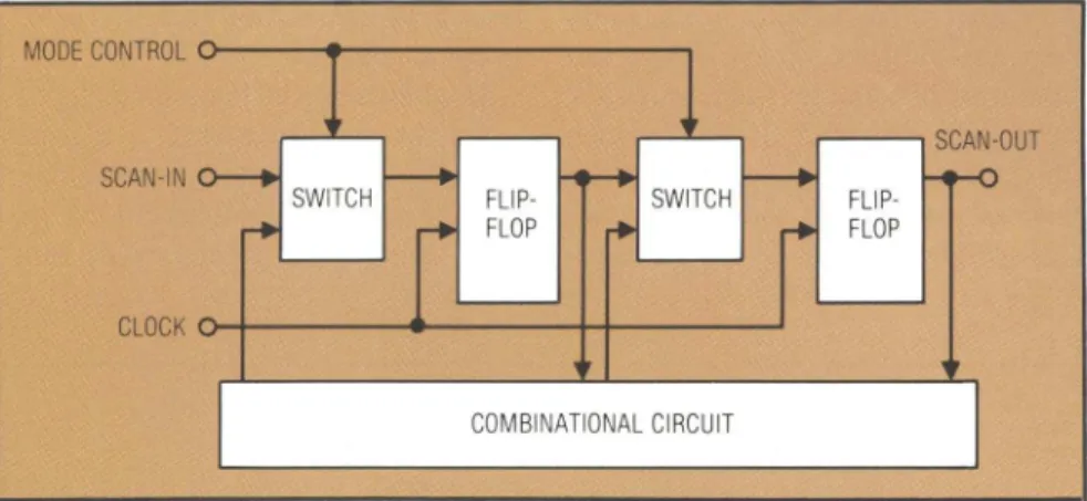
at thesametime, thev'are merged into oneprimarv input to reduce the num- ber of additional input points (Figure 2).Moreover, ifscan-pathtechnliqlS,
asshowniinFigure3,areused,one test
point wvillthen correspond toone flip- flop,and the increase in thenuimberof external points can be avoided.
We have investigated two methods ofalteringcircuitstofacilitatetestabil- itythroughthe addition oftest points.
Thefirst method is basedontestabilitv analvsis and involves the addition of test points to improve testability be- fore a test pattern is generated. Ob- tained results show that 100 percent test coverage within the allowed time limits is difficult to achieve with this method. The second method
emiploys
a test pattern generationalgorithm,
enablinig
us to generate a test pattern for any detectable fault wvithin the allowed time limits, andmaking
100 percenttest coveragepossible.Wepro-grammed the twomethods, and after
evaluating
some circuits with several thousandgates.,
vewereabletoobtain very favorable results wvith the second method. In thisarticle wveexamnineand compare these methods.Circuits considered here are com-
binational circuitsconsisting ofAND, OR, NOT, NAND, and NOR ele- ments, and faults are assumed to be Figure 1.Typesof test
points.sigetukaful.
DFT
through
testability analysis
To increase the effectiveness oftest pattern generation, testability mea-
sures, which express the ease or dif- ficulty of testing, are used in two al- gorithms: Podem7 and Fan,8 short forpath-oriented decision-makingand fanout-oriented test generation algo- rithm, respectively.
Herewedraw attentiontothe mea- surement of testability, and we de- scribe methods ofdesignmodification that facilitate testing through the im- provement oftestability. The overall
Figure2. Additionof test
points,
flow ofthese DFTmethodsis shown inFigure 4. Although theentire process could be automated, we have imple- mentedthesystem ininteractive form to improve efficiency by enabling the designer to input the choice ofsignal
lines needing improvement and the SWTC
FLOP
SWITCH FLIP-decision as to whether the desired degree of testability has been achieved. Testability analysis. Various mea-
sureshavebeen proposedasmeasures COMBINATIONALCIRCUIT
of testability.9-1 Here we use Gold- stein's measures,9 which express the
costs of controlling and observing. Figure3. Scan path method. Thus, to maximize testability, these
costs must be minimized. Goldstein proposed six measures in all, threeof whichapplytocombinationalcirciiits:
* [CC' (L)] The smallest number TsaiiyAayi
of signal lines which must have their logical values set in orderto
Coc fSga ie
setthe logical valueof signal lineL Choiceof Signal Lines for to 1; called signal line L's "I"
controllabilitycost.
* [CCO (L)] Defined in the same lec ionofTest Point
way as [CC' (L)]; called signal InsertionLocation
line L's "O"controllabilitycost.
* [CO (L )IThe smallest numberof nserionofTest Points
signal lines whichmust havetheir logical valuessetin orderto prop-
agatethe valueofsignal line L to Hasdesired
testabty
primaryoutput;called the observ- beenachieved?
abilitycost of signal lineL. Each of these valuescan be found for any given circuit through simple cal-E_D culations.
Selectionofsignallinesneedingim-
Figure
4. Work sequence in testability analysisDFr
method. provement. At this point the designercan see from the system the greatest controllability and observability cost values. Then hedecideswhether to im- prove thecontrollabilityortheobserv- ability and sets the threshold values. Values exceeding threshold valuesare then improved, starting from those nearestthe
primary input signal
line.Test point insertion locationsearch. Insertingtestpointsasshownin Figure I, a-c, markedlyimprovesthecontrol- lability for thesignal lines ontheout-
put side of the insertion point, leaving the input side
unchanged.
Accord- ingly, test points are inserted severalgates to the input side of signal lines Figure 5. Test point insertion location search.
with high controllability costs. Simi- duce here the method that was effec- neously high controllability cost. In larly, to improve observability, test tivein actual tests. the former case, it is best to insert atest pointsareinsertedseveralgatestothe Lookingatsignal line with highcon- point a bit further toward the input output sideofthesignallines withhigh trollability cost, we find two situa- side.Inthe latter case, insertionof the observability costs. The exact place- tions. Inthe first, oneofseveralinput test point is best on thesignal lineit- mentof test points is an extremely dif- lines dominates the others. In the sec- self. Space does not permit us to go ficultproblem, however, andweintro- ond, several input lines have simulta- into the standards used in deciding whetherwe arefaced with the firstor second situation, butwehave found it
generally
difficult to determine the mostsuitable standard.When asignal line has high control- lability cost, we find that either the observabilitycost drops
rapidly,
orit does not. With arapid drop,
we as-sume aproblemin
controllability,
andwe then search for aproper
point
of test-point insertion to lowerthe con- trollability cost (see Figure 5). Iftheobservability
costdoesnotdrop rapid-
ly,the next step is to analyze output. If no sudden drop in observability cost canbeseenallthe waythroughtothe primaryoutput,thenatestpoint
is in- sertedonthe original signalline a few gates towardthe outputside,asinFig-ure Id. Insertion so that the observ-
Figure 6. Test point insertion. ability costisonehalf of that for the
original signal linewasthemosteffec- tive.
Test point insertion methods. Fig-
ure6 shows one example ofan inser-
START
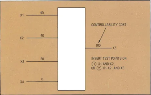
s_tion
location. The numbers appearing above each line express the control- labilitycosts. Inthisexample, thereis __ Ptomultiple inp gateGno
need to inserttest pointson inputinputside ofsignalline L lines Xltrollability cost on linethrough X4toX5.lowerInsertion ofthecon- twotestpoints,oneoneach of the lines Xl and X2 with poor controllability,
Can the method in or three test points on lines
Xl,
X2,igurelcbeapplied and X3, would be sufficient. This
Insert
testpoint
would spare us the problem of theasinFigurelc standardstobe
applied
wheninserting
Is thereanysingle _ _thetest point ontheinput line.
input gate onP? _ _ For the test point, a gate could be
added as shown in Figure la. How- ever, the addition of a gate would cause delay in a circuit designed for Inserttestpoint Insert test point high-speed operation, requiring a
asin Figurela asinFigurelb
redesign
ofthecircuit
withthe new test point. It is preferable, if possible, to use oneof the methods shown inFig-r END ure 1, b andc. Whenaddinga gate to
signal
lineL,wefollowthe flow chart in Figure 7 to determine whetherFigure 7. Selection of test point types. method lb orIccan be used.
Experimental results. After pro- all detectable faults. This method pays
fault;
when a fault isaborted,
it is gramming the design method de-special
attention toaborted faults oc- called at-difficult-to-test-for fault.
scribed above, we applied it to some
curring
after the test pattern genera- When noparticular
number ofback- circuits of several thousand gates and tionalgorithm
isapplied,
and it in- tracks isspecified,
tmaybe omitted. surveyed how the test coverage volves thesubsequent placement
of From theperspective
oftestpattern changed with the insertion of test testpoints
tomakesuch faults easiertogeneration,
aborted faults can bepoints. The computer used for our test. divided into threetypes:
calculationswasthe
large
computerat Types of aborted faults. With a test Fault type 1. An aborted fault Osaka University, an NEC System pattern generation algorithm that caused by difficulty in producing a 1000 (computation speed: 15 MIPS). sendsasignal whose value varies with faultysignal.
We used Fortran for programming, the existence or absence of a fault Fault type 2. A fault for which and for the test pattern generation (called a "faulty signal") along a faulty signal production is easy, but algorithm, we used the FAN algo- signal line on which a fault is inserted propagationof the
faulty signal
tothe rithm.8 Aborted faultswerethe faults (called a "faulty line"), we try prop- nextgate
isdifficult
ythat remained undetected after more agating a faulty signal from the faulty
Faun
t type 3.Afault
for which ob- thanThe100characteristics of thebacktrackoperations.circuits line to a primary output. When westart a backtrack cycle of a specificservation primary output
of theis faulty signal
difficult,even
atbeforedesigning fortestability arede- number(say100
times)
ofbacktracks,
though both the production and prop- scribed in Table 1. Test coveragewas t, the test pattern generation is agation of the faulty signal for more definedasfollows: aborted, indicating an aborted fault. than one gate were accomplished Testcomprehensiveness Wedifficultcanassumeto testfor.thatBelow,anabortedafault thatfaultis withoutdifficulty.
Number of detectedfaults ___ isnot
aborted-i.e.,
that doesnotap- Wecandetermine into whichof these Numberof detected faults + abortedfaults pear after alimited number of back-categories
the fault fallsby running
atracks,
t-is called a t-easily tested testpatterngeneration algorithm. Our findings are shownin thegraph inFigure8. Althoughtherearecases, as
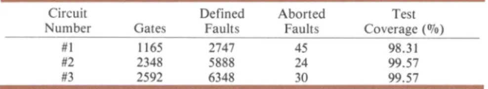
shownby circuit 3,where the insertion Table
1.
oftest points causes a clear drop in Characteristics of circuits before designing for testability. abortedfaults,therearealso cases,as
with circuit 2, where the addition of Circuit Defined Aborted Test
testpointsmakes thetestingmoredif- Number Gates Faults Faults
Coverage (%)
ficult. #1 1165 2747 45 98.31
Takingthese resultsasevidence,it is #2 2348 5888 24 99.57
clearthat themeasuresoftestabilitydo #3 2592 6348 30 99.57
notalways reflect theease or
difficulty
oftesting accurately.Also, although
the insertion oftestpointsclearly
im- proved testability, itwouldbeimpos- sibletosay that in allcasesthecircuithad been designed fortestability. \
DFT through test pattemr
generation algorithms
Asshown above, it is difficulttoob- tain complete test coverage with methodsbasedon
testability analysis.
In fact, for the number oftestpoints
added, thetestcoverage didnoteffec- tivelyimprove. Here,therefore,we ex- pand upon a method that ensures generation of test patterns for all detectable faults within the allowed computation time-in otherwords,
a method ofaddingtestpoints thatwillresult in 100 percent test coverage for Figure8.Experimentalresults oftestability analysismethod.
Insertion oftestpoints. Theoverall
START
~~~~~~~flow
is shown in Figure 9. The testpoints are of two types, showvn in
Generatepatterntest ~Figure 1, c and d. The following dis-
l 11|1 - for all faults _ cussion covers the methods of test
point insertion based on the type of aborted fault:
- allSlUck-PlaceCpericncesa
abortedtau
on (1)orte2 faultlist
_||LookigFault
t"ype
I. Test point insertionfollowstheflow chart inFigure 10,in- suringthat a
faulty
signa can e pro-selectt abortedsfault listanput duced without backtracking.
_tgenerat
clesttoprmatrnpt
_When we are tryingto assigna cer- tain value to a certain signal line, thevalueand the signal line are together ncalled an "objective." Several objec-
fault selected
tives held simultaneously are called a
"1setof
objectives."
Whensignal
linelexperiences a stuck-at fault at either0
nsert Insert or I in atype I fault, the initial objec-
s ing,
inttive
Tessis(0, L) or (I, L).st tLooking at the "type of
objective"
frame in Figure 10, wecan seethat for type(i),wecan meettheobjective byin- Select all faultstron serting a test
point
ofthe
type seen inaborted fault list and
Figure
Ic. For type (ii), the objective type 3 fault list and~~cannot
bemet. Fortype(iii), thesignal
generatetestpattern. line isaprimary
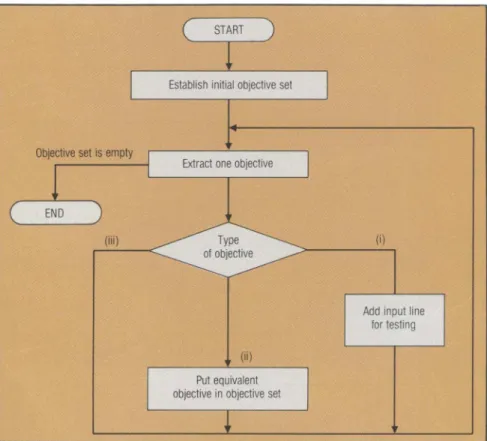
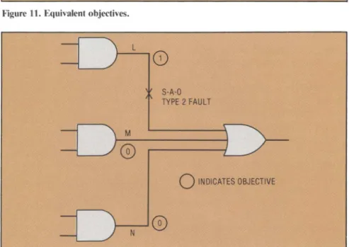
input,andnotestpoint is needed. With type(ii),weneedtoseeFigure9.Overallflow oftestpoint insertion, whattype ofvalueon theinput would enable the objective to be achieved. That value would be called the START
~~~~~~~~~~equivalent
objective" (Figure I1).After several test points have been inserted in accordance with the flow Etblishinitialobjectivese chartinFigure 10, theobjectivesetwill become empty andtheinsertion ofthe test points will be complete. For test-
ing, these input lines will become one
Extract one objective
~~~test
point according tothe circuitcon-struction in Figure 2.
Fauilt tYpe
2. Testpointinsertion for a type 2 fault is also carried out ac-.YV.
~~~~~~~~~cording
toFigure 10. However,thein-of objective
~~~~~~~itial
objectivesetis determined inadif- ferent manner from that for a type I fault.When,asinFigure
12,wehavea Addinputline stuck-at 0 fault onsignallineL,the in-testingfor itialobjective set is
~(I,L
),(0,M),
(0,N)Ptequivalent
Fut 'Ts on neto oobtectiveinobjectiveset
Faity~pe3.
Ts oitisrto oa type 3 fault is carried out only after testpointinsertion has beencompleted for fault types 1 and 2. Thetest
point
Figure10. Testpointinsertion fortypeI and type2 faults. usedisshowninFigure Id,andthefol-lowing procedures are followed to minimize the numberoftest pointsto be inserted:
First, for each
faulIt,
makea search forpossible locations that ensure that test point insertion facilitates detec- tion. Once located, a faulty signal should be produced and propagationattempted, inthesame manner as for Figure 11.Equivalent objectives.
classifying
aborted faults.Next,choose the smallestnimber of test point insertion locations that will enable all faults to be detected.
If we are to eliminate all aborted faultsby the above method, any fault occurring in the newlv added test points must be easily testable. Fol- lowingthe flow chart in Figure9, we can avoid a difficult-to-detect fault in the test points in the manner shown briefly belowv:
First, for the test point insertion shown in
Figuire
Ic, used with faulit types I and 2, consider the exarnple shownin Figure 13. Astuck-at0fault at test pointXisequivalentto astuck-at0 faultat Yand is thus easyto test
Figure
12. Initial objective fortype
2fault. for. A stuck-at 1 fauilt at X becomesredundant ifthestuck-at0faultat Yis redundant, andbecomes testableifthe stuck-at 0faultat Yis testable, because it can be tested by the same test pattern with X = 0. Thus, the stuck-at I fault at X can be seen as the equivalent of the stuck-at0faultat Y. Accordingly, the number of difficult-to-test-for
faults does not increase. Figure 13. Exampleoftestpointsfor faulttypesI and 2. Second,to usethe methodshown in
Figure Id for type 3 faults, consider the example shownin Figure 14. This type of test point insertion is carried outaftertypes I and 2 havebeen elim- inatedfrom the circuit. Accordingly, it iseasy to set signalline Yat either 0 or 1, making it easy to test signal line X.
Figure 14. Example of test points forfaulttype 3. Fxperimental results.The resultswe
obtainedfrom programming theDFT Table 2.
method incorporating a test pattern Results of design for testability withtest pattern generation algorithm. generation algorithm are shown in
Table 2. The computer, thelanguage, Circuit Computation Test
and theapplied circuits we used were Number Added Input AddedOutput Time(sec.) Coverage (o)
all the same as those we used for the #1 3 8 13.7 100.0
testability analysis method. As shown #2 1 6 11.3 100.0
inTable2,withthetestpatterngenera- #3 4 4 14.5 100.0
tion algorithm, circuits of from 1000 References 6. W.Coyand A.Vogel,"InsertingTest
to3000gateswere100percenttestable Points forSimpleTest Generation,"
with the addition of only about 10 test Proc. Fourth Intl Conf. Fault-
1. T. W. Williams and K. P. Parker, Tolerant
Systems
and Diagnostics, points. Theratiobetween the number "Design for Testability-a Survey," 1981, pp.180-186.
of the first aborted faults and the Proc. IEEE,Vol.71, No.1,Jan. 1983, 7. P. Goel, "An Implicit Enumeration number oftest points was3.4to4.1. pp.98-112. Algorithm to GenerateTests for
Com-
Compared with the resultsof thetest- . binational Logic Circuits," IEEE ability analysis method, insertion of 2. M- J. Wilhams and J. B. Angell, Trans. Computers, Vol.C-30,No.3, testpointswashighly effective.Integrated Circuits via Test
Point and Mar. 1981,pp. 215-222.Computation time. To lessen the Additional Logic," IEEE Trans. 8. H. Fujiwaraand T. Shimono, "On number oftestpoints,whenevera test Computers, Vol. C-22, No. 1, Jan. the Acceleration of Test Generation point ofthetype shown inFigure lc 1973,pp. 46 60. Algorithms," Proc. 13thFault Tolerant Computing, JuneInt'lConf. was inserted, test pattern generation 3. E. B. Eichelberger and T.
W.
1983, pp. 98-105; also IEEE Trans. wasconducted for all aborted faults. Williams, "A Logic Design Structure Computers, Vol. C-32, No. 12, Dec. Because of this, each circuit took 10-15 forLSI Testing," Proc. 14th Design 1983,pp. 1137-1144.seconds. Theprocesstookprecedence Automation Conf., June 1977, pp. 9. L. H. Goldstein, "Controllability/ over redesigning and comprised 7-30 462-468. Observability AnalysisofDigitalCir- percent of the time required for test 4 S F N cuits," IEEE Trans. Circuits and
patte genratin.Hweve, cosid- 4. S.Funasu, . Waatsui, ad T.
Systemzs,
Vol. CAS-26, No. 9, Sept.pattern generation. However, consid- *
Arima,
"TestGenerationSystems in
1979, pp.685-693.
ering that there isusuallynoguarantee Japan," Proc. 12th Design Automa- 10.
P. G. Kovijanic, "Testability
Analy- that test coverage will always be 100 tionSymp., June1975, pp. 114122. sis," Digest ofPapers,
1979 Test percent eveniftestpatterngeneration 5. J. P. Hayes and A. D. Friedman,Conf.,
pp.310-316.
time is extended by this amount, we "Test
Point Placement
to Simplify 11. H. Fujiwaraand H. Ozaki,"A
Newbelieve the time is a small price for FaultDetection," IEEE Trans.
Com-
Measure for Test Generation by a completetestcoverage. puters, Vol. C-23, No. 7, July 1974, Heuristic Method," IECE mono- Astotheexpenseinvolved in adding pp. 727-735. graph, EC80-38,Oct. 1980,pp. 1-8. hardware,weusedaverylow numberof test points and only those which could be realized at aminimumcost; thuswebelieve thatcostisnot agreat
problem.
A mong themethodswehave dis- cussedand mentionedhere,the methodutilizinga testpatterngenera- tion algorithm obtained the best resultsby far. We attribute thisto our useofadirect solutiontotheproblem
ofdifficult-to-test-for faults. [ AkiraMotohara is a graduate student in the HideoFujiwara has beenwith the Depart- Department of Electronic Engineering, ment of Electronic Engineering of Osaka Faculty ofEngineering, at Osaka Universi- University since 1974. In 1981 he was a ty. Hisresearch interests include test pat- visting assistant professor at theUniversity terngeneration, design for testability, logic ofWaterloo, and,in1984, avisitingassoci- simulation, and faultsimulation. ate professor at McGill University, Can- Hereceived the BE degree in electronic ada. His research interestsincludeswitch- engineering from Osaka University in1983. ing theory, design for testability, test He is amember ofthe Institute of Electron- patterngeneration, faultsimulation, built- ics and Communication Engineers of inself-test, and fault-tolerant systems.
ACknowledgments
Japan. Fujiwara received the BE, ME, and PhDWe wish to thank Hiroshi Ozaki, pro- degrees in electronic engineering from
fessor emeritus at Osaka University, for his OsakaUniversityin 1969, 1971, and 1974
support andencouragement of thiswork. respectively. Hewasmember of the Tech-
We also thank the members of the sixth nical ProgramCommittee ofthe 1982 In-
chair of the Department of Electronic ternational Symposiumon Fault-Tolerant
Engineering, Osaka Univeristy, for their Computing. He received an Institute of
valuable discussions. Special thanks to Electronics and CommunicationEngineers
Kenjiro Sasaoka (presently with MITI) for Theauthors' address is Department of Young Engineer Award in 1977. He isa the testabilityprogramming aswellas the Electronic Engineering, Faculty of Engi- senior memberoftheIEEE, a member of results of the test pattern generationexperi- neering, Osaka University, 2-1 Yamada- the IECEof Japan, and a member of the ment. Oka, SuitaCity,Osaka 565, Japan. InformationProcessingSocietyofJapan.