BIST Pretest of ICs: Risks and Benefits
Yoshiyuki Nakamura
1,2, Jacob Savir
3and Hideo Fujiwara
11
Nara Institute of Science and Technology, Ikoma, Nara, 630-0192 Japan
2
NEC Electronics Corporation, Kawasaki, 211-8668 Japan
3
New Jersey Institute of Technology, Newark, NJ 07102-1982
[email protected], [email protected], [email protected]
Abstract
The object of this paper is to analyze the potential ben- efits of conducting a BIST pretest before launching a func- tional test of ICs during post manufacturing screening. In [1] the impact of BIST on the chip defect level after test has been addressed. It was assumed in [1] that no measures are taken to assure that the BIST circuitry is fault-free before launching the functional test. In this paper we assume that a BIST pretest is first conducted in order to rid of all chips that fail it. Only chips whose BIST circuitry has passed the pretest are kept, while the rest are discarded. The BIST pretest, however, is assumed to have only a limited cover- age against its own faults. This paper studies the product quality improvements as induced by the BIST pretest, and provides some insight as to when this pretest maybe worth- while performing. As the study shows, in many cases the potential benefits outweigh any potential risks.
1. Introduction
Williams and Brown [2] had shown the relationship be- tween the product defect level, the manufacturing yield, and the fault coverage of the test process used to screen it into either a good lot or a bad lot. This well-known relationship is derived assuming that the test equipment is fault-free.
Many chips today have built-in self-test (BIST) circuitry in them. These BIST circuits are used to test the chips and perform the screening [3]. Since the BIST hardware is manufactured using the same technology and process as the functional circuits, it is unrealistic to assume that it is fault- free. Moreover, chip manufacturers do not insert any redun- dancy into their BIST hardware for the sake of keeping the cost down. As a result, the BIST hardware is not made to be fault-tolerant. It is, therefore, imperative to allow the BIST hardware to be subjected (during the analysis) to the same defect density as the functional circuits themselves.
Nakamura et. al. [1] have derived formulas to assess the impact of the BIST circuitry on the final integrated circuit (IC) defect level after test. The authors in [1] assume that no measures are taken to assure that the BIST circuitry is, in fact, working properly before the initiation of the functional test4. The formulas derived in [1] show a considerable de- parture from those in [2].
In this paper we assume that a BIST pretest is first con- ducted in order to rid of all chips that fail it. Only chips whose BIST circuitry has passed the pretest are kept, while the rest are discarded. The BIST pretest, however, is as- sumed to have only a limited coverage against its own faults. The reason for this is that only primitive operations, such as scan and capture, are possible during pretest. A more com- prehensive BIST pretest will require the use of external test equipment, which defeats the incentive for BIST altogether. Thus, only a subset of chips with faulty BIST can be iden- tified and eliminated. Chips with faulty BIST that escape the pretest are used later on to conduct the functional test. Generally speaking, therefore, there are two side effects re- sulting from this BIST pretest. One side effect is to cause a good product (i.e. no functional defects present) to be dropped, resulting in a yield loss. A second side effect is to have a bad product be passed as good by a faulty BIST during the functional test, increasing the shipped-product defect level. References [4-8] discuss multitude of subjects relating to yield, fault coverage and defect level after test.
This paper is organized as follows. Section 2 is a brief review of the earlier results reported in [1][2]. Section 3 de- rives the defect equations in BISTed products that have un- dergone both a pretest and a functional test. We show that the Williams and Brown’s equations [2] and the Nakamura et. al. equations [1] are special cases of our more gener- alized formulas. Section 4 discusses the properties of the newly derived formulas by displaying the graphs of some
4In this paper functional test means a CUT BIST test, to distinguish it from the BIST pretest.
IEEE 24th VLSI Test Symposium (VTS'06), pp. 142-147, May 2006.
typical case studies. The case studies involve both an early life phase, and a product maturity phase. Section 5 draws some conclusions from this study.
2. Recapitulation of earlier results
Let the circuit under test (CUT) havencpossible faults, each having the same probability of occurrence, p. The yield,Y , is the probability that the circuit is fault-free, i.e.
Y = (1 − p)nc. (1)
The raw defect level of the product coming out of the man- ufacturing line (without any test) is
D0= 1 − Y = 1 − (1 − p)nc. (2) Williams and Brown [2] analyzed the defect level of the product after test, under the assumption that the test pro- cess is fault-free. Assuming that the test process can detect m out of the ncpossible faults, the fault coverage against functional faults is given by
F = m nc
. (3)
A circuit that passes the test is guaranteed to be free of any covered faults (m in total), but can still possess an uncov- ered fault that escaped the test. The defect level after test was derived in [2], and is given by
D = 1 − Y1−F. (4)
The work of Williams and Brown was extended in [1] for ICs having BIST circuitry in them. The BIST circuitry is used to test the functional circuits and screen them into ei- ther a good lot or a bad lot. The underlying assumption in [1] was that the BIST circuitry is unreliable, i.e. it is pos- sible for the BIST circuitry itself to be faulty. The reason for this assumption is that the BIST circuitry is manufac- tured using the same technology as the functional circuits themselves, and therefore is subjected to the same process impurity. The effects of using this unreliable BIST circuitry as a test vehicle where analyzed in [1], and are repeated here for the reader’s convenience.
The defect level after test in BISTed products is given by
D′= 1 − Y1−F′, (5)
whereF ’ is the effective CUT fault coverage as conducted by the BIST circuitry, and is given by
F′= F [Yα+ ρ(1 − Yα)]. (6) The parameter α is the ratio between the BIST circuitry area and the area of the CUT. The parameter ρ is the CUT fault
coverage alteration factor. Notice that ρ can be larger than 1. The reason for this is that it is possible for a BIST fault to create a situation where every CUT, good or bad, is re- jected by the test. We refer to this case as a catastrophic case. Thus, the largest ρ may become isnc/m = 1/F . The possible range for ρ is, therefore,0 ≤ ρ ≤ 1/F .
The impact of the BIST impurity on the product defect level can be best measured by the differential∆D′= D′− D, or, equivalently, by its normalized form, ∆D′/D. When a product manufacturing process reaches maturity, its yield is close to 1. Furthermore, in most real–life cases F′ ≈ F , α << 1. The normalized surge in product defect level under these conditions is approximately:
∆D′
D ≈
F α(1 − ρ)(1 − Y )
1 − F . (7)
3. Effects of BIST pretest
3.1. AnalysisIn this case the BIST circuitry undergoes an operation pretest in order to discard of any chips with faulty BIST in them. This pretest, however, is conducted by the BIST cir- cuitry itself, and is far from being comprehensive. In this primitive test, the LFSRs/MISRs are cycled, starting with a known seed, to see if they can end up with a correct sig- nature after a predetermined number of clocks. BIST cir- cuitry that passes this pretest is by no means guaranteed to be fault-free. BIST circuitry that passes this test can still possess, for example, interconnect faults between the LF- SRs/MISRs and the CUT. This pretest, therefore, has rel- atively low fault coverage against its own faults. The rea- son why a primitive, rather than a comprehensive, pretest is conducted is that the latter requires the use of external test equipment that totally defeats the purpose of BIST to begin with.
We use the following notations in the following analysis: D - Product defect level after test under fault-free BIST
hardware
D′ - Product defect level after test under unreliable BIST hardware and without BIST pretest
D′′ - Product defect level after test under unreliable BIST hardware and with BIST pretest
F - Fault coverage of the CUT under fault-free BIST hard- ware
F′ - Effective fault coverage of the CUT in the presence of an unreliable BIST hardware and without BIST pretest F′′ - Effective fault coverage of the CUT in the presence of
an unreliable BIST hardware and with BIST pretest Y - Product yield
p - Fault probability
nc - Total number of possible faults in the CUT
nb - Total number of possible faults in the BIST hardware m - Number of CUT faults covered by fault-free BIST
hardware
mb - The number of BIST circuitry faults covered by the BIST operation pretest
m′ - Expected number of CUT faults covered by an unreli- able BIST hardware and without BIST pretest m′′ - Expected number of CUT faults covered by an unre-
liable BIST hardware and with BIST pretest
k - Expected number of CUT faults covered by a faulty BIST hardware and without BIST pretest
k∗ - Expected number of CUT faults covered by a faulty BIST hardware and with BIST pretest
α - Ratio between BIST area and the CUT area
ρ - CUT Fault coverage alteration factor without BIST pretest
ρ′ - CUT Fault coverage alteration factor with BIST pretest µ - BIST circuitry fault coverage during pretest
λ - Yield coefficient
Let k be the expected number of CUT faults detected by a faulty BIST that did not undergo an operation pretest. Letk∗be the expected number of CUT faults detected by a faulty BIST that passed the operation pretest.
The parameter ρ is the CUT fault coverage alteration factorwithout BIST pretest [1], and is given by,
ρ= k
m (0 ≤ ρ ≤ 1/F ),
The parameter ρ′is the CUT fault coverage alteration fac- torwith BIST pretest, and is given by,
ρ′= k
∗
m (0 ≤ ρ
′≤1/F ).
We proceed to calculatem′′, the expected number of CUT faults covered by BIST. Since the BIST circuitry that con- ducts the CUT test has passed the operation pretest, it is guaranteed to be free of thembfaults covered by it. There- fore,
m′′= m×Pr{Fault-free BIST}+k∗×Pr{Faulty BIST}, m′′= m(1 − p)nb−mb+ k∗[1 − (1 − p)nb−mb]. (8) The expected CUT fault coverage, as conducted by the BIST circuitry, is:
F′′=mnc′′=nmc(1−p)nb−mb+kn∗c[1−(1 − p)nb−mb]
=nmc{(1−p)nb−mb+km∗[1−(1−p)nb−mb]},
which can further be written as:
F′′= F!Y nb−mbnc + ρ′(1 − Ynb−mbnc )". (9) The exponent in Eq. (9) can be written as
nb−mb
nc
= nb nc
(1 −mb nb
) = α(1 − µ),
where α= nb/nc, and µ = mb/nb.
We define λ= α(1 − µ). We call λ the yield coefficient, 0 ≤ λ ≤ 1. The parameter µ is the BIST circuitry fault coverage during the pretest.
The effective fault coverage,F′′, can now be written as F′′= F [Yλ+ ρ′(1 − Yλ)], (10) and the defect level after the CUT functional test becomes
D′′= 1 − Y1−F′′. (11) Example 1: Consider a chip manufacturing line with 90% yield. The chips are screened using their BIST circuitry. The BIST circuitry constitutes 5% of the entire chip area. The BIST procedure has 95% coverage of the functional faults when assumed to be fault-free, and only 40% cover- age when assumed faulty. Let the BIST circuitry undergo a pretest with self-fault coverage ofµ = 0.3. All chips failing the pretest are discarded. The chips passing the pretest are kept and used to perform the BIST CUT test. Chips that fail the CUT test are discarded. Compute the defect level of the chips passing both tests.
Solution: We have the following parameters: α= 955 = 191, µ = 0.3,
λ= 0.719 ≈3.68 × 10⁻², ρ′= 4095 ≈0.421, F′′= 0.95×[0.93.68×10−2+0.421×(1−0.93.68×10−2)]
≈0.9479,
D′′≈1−0.91−0.9479≈1−0.90.0521≈5.474×10⁻³
≈5474ppm,
which is 95ppm smaller than the detect level obtained with- out a pretest for the same parameter values [1]. ! It is interesting to take note of the following special cases:
If there is no BIST circuitry (α= 0), we have F′′= F , andD′′= D. This is the Williams and Brown’s case. Also, in the case of an ideal BIST pretest, we haveµ = 1. In this case also, the formulas reduce to the Williams and Brown’s case. The reason for this is that when µ = 1 the BIST
pretest is able to rid of all the chips with faulty BIST hard- ware. The CUT, therefore, is tested by a reliable “tester”, which was the underlying assumption used by Williams and Brown in the first place.
If the BIST procedure has zero coverage against func- tional faults while being itself faulty, then ρ′ = 0. The effective fault coverage, in this case, reduces to:
F′′= F Yλ. (12)
Note that the case ofµ = 0 is the case of a “pretest with no coverage against its own faults”. This is, therefore, iden- tical to the case of CUT screening without a BIST pretest. The formulas in this case reduce to those derived in [1], and shown earlier in section 2 for the reader’s convenience.
We measure the impact of the BIST impurity on the product defect level by the differential∆D′′ = D′′−D, or, equivalently, by its normalized form,∆D′′/D. When a product manufacturing process reaches maturity, its yield is close to 1. Furthermore, in most real-life casesF′′ ≈ F , λ << 1. By using calculus approximation techniques we get two sets of approximation formulas. The first set:
∆D′′≈F λ(1 − ρ′) ln2Y, (13) and
∆D′′
D ≈
F λ(1 − ρ′) ln2Y
(1 − F )(1 − Y ) . (14) The second set of formulas can be obtained from the first set by lettingln Y ≈ −(1 − Y ):
∆D′′≈F λ(1 − ρ′)(1 − Y )2, (15)
∆D′′
D ≈
F λ(1 − ρ′)(1 − Y )
1 − F . (16)
For the catastrophic case (ρ′ = 1/F ), we get from Eqs. 15 and 16:
∆D′′|cat ≈ −λ(1 − F )(1 − Y )2, (17)
∆D′′ D
#
#
#
#cat
≈ −λ(1 − Y ). (18)
3.2. Sizing the effect of the BIST pretest It is interesting to assess the influence of the BIST pretest on the shipped-product defect level. To assess this impact we compute the difference in∆D/D with and without the BIST pretest. This will help determine if the alteration in product defect level, achieved as a result of the BIST pretest, is worth the added risk of having to compromise the loss in product yield.
Let δD be the difference between the two defect level differentials with and without a BIST pretest. Let δD/D
denote the difference between the two normalized differen- tials (normalized against the Williams and Brown’s case). We, therefore, have:
δD = ∆D′−∆D′′.
At maturity, and under relatively high fault coverages, we get:
δD ≈ F α[µ(1 − ρ′) + (ρ′−ρ)] ln2Y, (19) and
δD
D ≈
F α[µ(1 − ρ′) + (ρ′−ρ)] ln2Y
(1 − F )(1 − Y ) . (20) There is no good reason whyk∗should (statistically) be any different fromk. The reason for this is that the BIST op- eration pretest will only guarantee that those who pass it are free of some, but not all, of the totality of possible faults. The eliminated BIST faults will remove some faults with detectability larger thank, and some faults with detectabil- ity smaller thank, not affecting (in principle) the average k.
By lettingk∗≈k we get ρ′≈ρ. In this case we, there- fore, get:
δD ≈ F αµ(1 − ρ) ln2Y, (21) and
δD
D ≈
F αµ(1 − ρ) ln2Y
(1 − F )(1 − Y ) . (22) By lettingln Y ≈ −(1 − Y ) in Eq. (22) we get:
δD
D ≈
F αµ(1 − ρ)(1 − Y )
1 − F . (23)
For the catastrophic case (ρ= 1/F ), we get from Eq. 23: δD
D
#
#
#
#cat
≈ −αµ(1 − Y ). (24)
Example 2: As a continuation of Ex. 1, we use Eqs. 21, and 22 to assess the BIST pretest impact on the final product defect level:
Solution: We have:
δD ≈ .95×.0526×.3×(1−.421)×ln20.9 = 96ppm. Compare this to the 95ppm computed in Ex. 1. Similarly,
δD
D ≈
δD
(1 − 0.95)(1 − 0.9)≈0.019,
which is less than 2%. !
4. Some typical behavior
During the product’s early life its yield is relatively low. This is mostly due to not quite knowing how to best fine- tune the manufacturing parameters of an emerging new technology. Typical early life yields may vary between 40% to 60%, even though lower figures are also possible. As the manufacturing process matures, the yield figures may rise to as much as 90%, or even higher. In this section we try to shed some light on the impact of the BIST pretest during these two distinct periods of the product’s life. The param- eters chosen in this study reflect likely operating conditions of an IC manufacturing fab. In the following study we as- sume ρ′≈ρ.
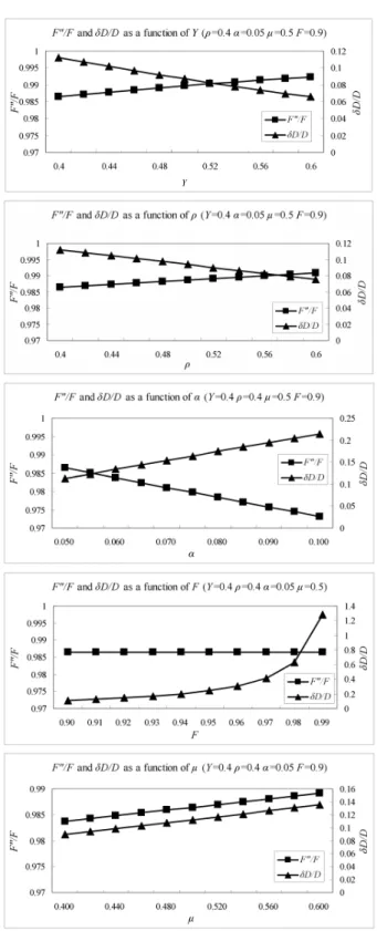
In Fig.1 we show the behavior ofF′′/F and δD/D dur- ing the product’s early life. In order to study the impact of the BIST pretest on the product’s early life defect level after the CUT test, we let 0.4 ≤ Y ≤ 0.6. The other parameter ranges are0.9 ≤ F ≤ 0.99, 0.4 ≤ ρ ≤ 0.6, 0.05 ≤ α ≤ 0.1 and 0.4 ≤ µ ≤ 0.6.
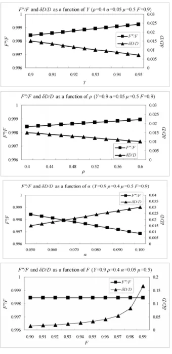
In Fig.2 we show the behavior ofF′′/F and δD/D at maturity stage. Since at maturityY ≈ 1, we plot F′′/F and δD/D for the parameter ranges 0.9 ≤ Y ≤ 0.95, 0.9 ≤ F ≤ 0.99, 0.4 ≤ ρ ≤ 0.6, 0.05 ≤ α ≤ 0.1 and 0.4 ≤ µ ≤ 0.6.
As was mentioned earlier, by discarding of chips that fail the pretest we are risking loosing products that would oth- erwise be functional. This will, undoubtedly, increase the yield loss. Given the fact that the pretest will not rid of all chips with faulty BIST circuitry, some people may argue that this pretest is not worth the risk of loosing yield.
As seen in the Fig. 2, unless the CUT fault coverage is in the high 90 percent, the pretest won’t buy you much qual- ity improvement during maturity. For CUT fault coverages below 98% the impact of the pretest on the product defect level is quite minor (around 2%). This quality improvement grows substantially when the CUT fault coverage exceeds 98%, and can be as high as 20-30%.
During early life the BIST pretest has a greater effect on the product defect level. Even for CUT fault coverages around 90%, the BIST pretest can decrease the product de- fect level by as much as 10%. This quality improvement grows to 80% for fault coverages around 98%.
5. Conclusions
In this paper we assume that the BIST circuitry is pretested before launching the CUT functional test. The intent of the BIST pretest is to rid of all chips that fail it, and, therefore, avoid a situation where a faulty BIST has to determine whether or not the functional circuits operate correctly. By discarding of chips that fail the pretest we are risking loosing chips that would otherwise be functional.
Figure 1.F′′/F and δD/D at early life
Figure 2.F′′/F and δD/D at maturity stage
This will, undoubtedly, increase the yield loss. Given the fact that the pretest will not rid of all chips with faulty BIST circuitry, some people may argue that this pretest is not worth the risk of loosing yield. This paper provides some insight as to when this BIST pretest maybe worthwhile.
We show that the BIST pretest has an effect of reducing the product defect level of chips passing the CUT BIST. The question is whether or not the improvement in the shipped- product defect level is worth loosing functional chips as well.
Our analysis indicates that for products with CUT fault coverages exceeding 98%, it makes sense to do the BIST pretest. The BIST pretest has the effect of reducing the product defect level by at least 80% during early life, and by as much as 10% during maturity.
During early life, and even for fault coverages below 98%, the BIST pretest offers a non-negligible improvement in product quality. Since this improvement can be as small as 20-30%, and as high as 100%, BIST pretest is worthwhile performing.
Acknowledgments
This work was supported in part by Japan Society for the Promotion of Science (JSPS) under Grants-in-Aid for Sci- entific Research B(2)(No. 15300018). The authors would like to thank members of Fujiwara Laboratory of NAIST who have given their valuable comments.
References
[1] Y. Nakamura, J. Savir and H. Fujiwara, “Defect Level vs. Yield and Fault Coverage in the Presence of an Unreliable BIST,” IEICE Trans. on Inf. and Syst., vol. E88-D, No. 3, pp. 610-618, 2005.
[2] T.W. Williams and N.C. Brown, “Defect Level as a Func- tion of Fault Coverage,” IEEE Trans. on Comput., vol. C-30, No.12, pp. 987-988, 1981.
[3] P.H. Bardell, W.H. McAnney and J. Savir, “Built-in Test for VLSI: pseudorandom techniques,”Wiley Interscience, 1987. [4] J. Savir, “AC Product Defect Level and Yield Loss,” IEEE Trans. on Semiconductor Manufacturing, vol. 3, No. 4, pp. 195-205, 1990.
[5] J. Savir, “AC Product Defect Level and Yield Loss,” Proc. 1990 Int. Test Conf., pp. 726-738, 1990.
[6] F. Corsi, S. Martino and T.W. Williams, “Defect Level as a Function of Fault Coverage and Yield,” Proc. European Test Conf., pp. 507-508, 1993.
[7] P.C. Maxwell, R.C. Aitken and L.M. Huisman, “The Effect on Quality of Non-Uniform Fault Coverage and Fault Prob- ability,” Proc. Int. Test Conf., pp. 739-746, 1994.
[8] E.S. Park, M.R. Mercer and T.W. Williams, “Statistical De- lay Fault Coverage and Defect Level for Delay Faults,” Proc. Int. Test Conf., pp. 492-499, 1988.