Secure and Testable Scan Design Using Extended de Bruijn Graphs
Abstract - In this paper, we first introduce extended de Bruijn graphs to design extended shift registers that are functionally equivalent but not structurally equivalent to shift registers. Using the extended shift registers, we present a new secure and testable scan design approach that aims to satisfy both testability and security of digital circuits. The approach is only to replace the original scan registers to modified scan registers called extended scan registers. This method requires very little area overhead and no performance overhead. New concepts of scan security and scan testability are also introduced.
I. Introduction
Increasing complexities in VLSI designs have raised concerns on the reliability of digital circuits. Design for testability (DFT) provides a solution to easily test digital circuits for faults. The most popular DFT technique that ensures high testability and yields high fault coverage is Scan Design. Scan test provides high controllability and observability over a chip, which makes testing the circuit easier. However, this makes reverse engineering of the chip much simpler as well. With improved control and access to the chip, vulnerability to attacks also increases. Due to this, scan chains can be used to steal important information such as intellectual property (IP) and secret keys of cryptographic chips [7]. The possibility of scan-based side-channel attacks adds to an already growing customer concern of hardware security. Fundamentally, the problem lies on the inherent contradiction between testability and security for digital circuits. Hence, there’s a need for an efficient solution such that both testability and security are satisfied.
Several works have been proposed to solve this challenging problem. A scan-chain design based on scrambling was proposed in [4], [5]. In this method, flip-flops are dynamically reordered in a scan chain. An alternative is given in [6], [7] where a secure scan-chain architecture with mirror key register (MKR) was introduced. Having both secure and insecure modes, any crypto chip with the proposed architecture can be switched between test/normal mode (insecure) and normal mode only (secure). Another scheme is the lock & key security technique proposed in [8], [9]. This technique divides the scan chain into smaller subchains of equal length. It uses a test security controller (TSC) to switch between secure and insecure modes. A superior method compared to the others mentioned is proposed by Paul et al. in [10]. It is a Vlm-Scan that utilizes some flip-flops in a scan chain for authentication to move to test mode. The circuit can proceed to test mode only if the proper sequence of test keys
are scanned in to the used flip-flops. It is better because the test controller can be tested, however, a long test key sequence is still needed. In [11], Sengar et al. discussed a model called secured flipped- scan-chain, which uses inverters in the scan path for protection. The design works as conventional scan chains do and there are no additional test keys or clock cycles. The architecture can also be tested the same way with scan chains, with additional NOT gates. However, despite the sufficient number of inverters, their positions can still be determined by simply scanning out after resetting (to zero) all the flip-flops in the scan chain. Thus, the internal state can be identified and the security is breached.
All of the said approaches, except the last one, add extra hardware outside of the registers. This entails several disadvantages such as high area overhead, timing overhead or performance degradation, increased complexity of testing, and limited security for the registers part among others. Our approach to secure scan design is only to replace the original scan registers with modified scan registers, which we call extended scan registers based on extended de Bruijn graph. The modification of scan registers requires little area overhead and no performance overhead with respect to normal operation. Moreover, we have considered preventing possible attacks to our system.
This paper is organized as follows. In Section II, we define and discuss the extended de Bruijn graph and the three extended scan register types based on it. In Section III, we define scan-security and scan-testability. Moreover, we provide explanation on the need for both and the contradiction between them. In Section IV, we present the proposed secure scan design according to the four extended scan register types. Furthermore, we discuss the scan-security and scan-testability of the proposed methods. Finally, our conclusion is provided in Section V.
II. Extended de Bruijn Graphs
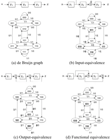
A de Bruijn graph represents a state transition graph of a shift register. Figure 1(a) illustrates a 3-stage shift register and the de Bruijn graph. Based from this, we define extended shift registers (or extended de Bruijn graphs) in the following:
Definition 1: Input-Equivalence. A k-stage extended shift register is called input-equivalent to the k-stage shift register if the state transition graph of the extended shift register is isomorphic to that of the shift register and the input assignment of the extended shift register is the same as
Hideo Fujiwara and Marie Engelene J. Obien
Graduate School of Information Science, Nara Institute of Science and Technology Kansai Science City, Nara, 630-0192 Japan
{fujiwara, obien-j}@is.naist.jp
that of the shift register. (State and output assignments are not necessarily the same.)
Definition 2: Output-Equivalence. A k-stage extended shift register is called output-equivalent to the k-stage shift register if the state transition graph of the extended shift register is isomorphic to that of the shift register and the output assignment of the extended shift register is the same as that of the shift register. (State and input assignments are not necessarily the same.
Definition 3: Functional Equivalence. A k-stage extended shift register is called functionally equivalent to the k-stage shift register if the state transition graph of the extended shift register is isomorphic to that of the shift register and the input and output assignments are the same as those of the shift register. (State assignment is not necessarily the same.)
(a) de Bruijn graph (b) Input-equivalence
(c) Output-equivalence (d) Functional equivalence Figure 1. de Bruijn graph and extended de Bruijn graphs
Figure 1(b)-(d) shows examples of extended de Bruijn graphs of input-equivalence, output-equivalence and functional equivalence, respectively. Underlined symbols indicate differences from the de Bruijn graph shown in Figure 1(a).
These extended de Bruijn graphs or extended shift registers can be realized by the following models: inversion inserted shift registers (I2SR), linear feed-forward shift registers (LF2SR), and linear feedback shift registers (LFSR). Besides those structures, extended de Bruijn graphs or extended shift registers can be realized by general sequential circuit structure. However, we consider I2SR, LF2SR and LFSR because of several advantages; easy design, easy
test, etc. These are defined and discussed in detail in the following.
Figure 2. I2SR with even number of inversions
(a) Input-equivalent (b) Output-equivalent Figure 3. I2SR with odd number of inversions A. I2SR
An inversion inserted shift register (I2SR) is obtained by inserting some inversions in a shift register. Figure 2 shows a 3-stage I2SR with even number of inversions. We can see it is functionally equivalent to the 3-stage shift register. Figure 3 shows a 3-stage I2SR with odd number of inversions. The state transition graph can be drawn in two ways as shown in the figure (a) and (b). Although they look as if they are different, they are identical. From these two state transition graphs, we see that it is input-equivalent and output-equivalent but not functionally equivalent.
Theorem 1: Any k-stage I2SR with even number of inversions is functionally equivalent to the k-stage shift register. Any k-stage I2SR with odd number of inversions is not functionally equivalent to the k-stage shift register but can be input-equivalent and output-equivalent.
B. LF2SR and LFSR
Any k-stage LF2SR is input-equivalent to the k-stage shift register, but it is not always output-equivalent. As shown in Figure 4(a), the state transition graph of the LF2SR is isomorphic to that of the shift register and the input assignment is also the same, hence input-equivalent. Nevertheless, the state assignment and output assignment are different from those of the shift register, as indicated by the underlined assignment. Therefore, this LF2SR is not output-equivalent though it is input-equivalent.
However, this can be modified to be output-equivalent by manipulating the linear sum of the output. From Figure 4(a), the output assignment is different from that of the 3-stage shift register only when state transition occurs from
states (011), (010), (110), and (111), i.e., only when y2 is 1. Hence, as shown in Figure 4(b), by adding an XOR at the output with inputs from y3 and y2 that is indicated by the broken line arrow, the output assignment of the modified LF2SR becomes the same as that of the shift register of Figure 1(a). With this, only the state assignment is different while the input and output assignments remain the same, thus making the LF2SR functionally equivalent.
Theorem 2: Any k-stage LF2SR is input-equivalent to the k-stage shift register. Although an LF2SR is not always output-equivalent, it can be modified to an LF2SR that is output-equivalent (and hence functionally equivalent) to the k-stage shift register, by manipulating the linear sum of the output.
Similarly, the following theorem for LFSR holds. Theorem 3: Any k-stage LFSR is output-equivalent to the k-stage shift register. Although an LFSR is not always input-equivalent, it can be modified to an LFSR that is input-equivalent (and hence functionally equivalent) to the k-stage shift register, by manipulating the linear sum of the input.
(a) Not output-equivalent (b) Modified Figure 4. Extended de Bruijn graphs for LF2SR
Figure 5. Proposed scan design with ESR
It might be hard to construct a long stage of extended shift register that is functionally equivalent to the same stage of shift register. To overcome this, the following theorem is useful.
Theorem 4: Let R1 and R2 be k1-stage and k2-stage extended shift registers that are functionally equivalent to k1-stage and k2-stage shift registers, respectively. Then, a cascade of R1 and R2 becomes a (k1+ k2)-stage extended shift register that is functionally equivalent to the (k1+ k2)-stage shift register.
Given these extended shift registers, we can arrive at a secure scan design, which is scan-secure and scan-testable. These terminologies will be discussed in the next section.
III. Security and Testability
A scan-designed circuit consists of a single or multiple scan registers and the remaining combinational logic circuit (kernel). A scan register is regarded as a shift register with multiplexers that select the normal data from the combinational logic circuit and the shifting data from the preceding flip-flop. Here, we replace the shift register with an extended shift register. The scan register with the extended shift register as shown in Figure 5 is called the extended scan register (ESR).
Scan registers or scan chains are proven to be effective in improving the testability of digital circuits. However, its effect on the circuit, which makes its registers easily accessible from primary inputs and outputs, allow attackers to exploit this opportunity to extract key streams, copy intellectual property (IP), and even manipulate the circuit. This makes it difficult for scan chains to be used especially in special cryptographic circuits where secret key streams are stored in internal registers, thus a problem in testing these types of circuits is imminent. However, quality of these circuits is highly in demand currently due to increase in the need of secure systems.
Our secure scan design through ESR provides both security and testability. With the same effectiveness and efficiency of conventional scan design and with very minimal overhead, any digital circuit can be both easily testable and secure against attackers.
When we consider a secure scan design, we need to assume what the attacker knows and how he can potentially make the attack. Here, we assume the following.
1. The attacker does not know the detailed information in the gate-level design.
2. The attacker knows the cryptographic algorithm implemented in the circuit or the general implementation structure at high level so that he can make bit-change insertion attack or differential values attack [6,7].
3. The attacker knows the presence of test pins (scan-in/out, scan, and reset) and scan chains (ESR). However, he does not know the structure of ESR (the connection information, positions of XOR and NOT, and the size).
Based on the above assumptions, we define the security to prevent scan-based side-channel attacks.
Definition 4: Scan-Security. A circuit with ESR is called to be scan-secure if the attacker cannot uniquely determine the structure of the ESR and hence the state-assignment of the ESR. An extended shift register R is called to be scan-secure if R is an extended shift register of a scan-secure circuit with ESR.
The structure of the ESR is important to the attacker in order to understand the scanned out values from the registers, which can reveal the key stream or the initial values of the internal registers, once computed. Thus, the level of security is dependent on the difficulty of determining the ESR structure. If the attacker cannot identify the structure of the ESR, the internal register values cannot be retrieved. Despite numerous attempts to apply input patterns, since the
output would remain the same as it would for conventional scan, it would be difficult for the attacker to access important information from the circuit.
Definition 5: Scan-Controllability. An extended shift register R is called to be scan-controllable if for any internal state of R a transfer sequence (of length k) to the state (final state) can be generated only from the connection information of R, independently of the initial state, where k is the size of R. A circuit with ESR is called to be scan-controllable if the extended shift register of the ESR is scan-controllable.
Definition 6: Scan-Observability. An extended shift register R is called to be scan-observable if any present state (initial state) of R can be identified only from the output sequence (of length k) and the connection information of R, independently of the initial state and the input sequence, where k is the size of R. A circuit with ESR is called to be scan-observable if the extended shift register of the ESR is scan-observable.
Definition 7: Scan-Testability. An extended shift register R is called to be scan-testable if R is scan-controllable and scan-observable. A circuit with ESR is called to be scan-testable if the extended shift register of the ESR is scan-testable.
Scan-controllability is the simplicity and easiness of generating the transfer sequence of a circuit to any desired state. The transfer sequence can be obtained only by using the information of ETS, and the length of the transfer sequence is the size of ESR, i.e., the number of flip-flops. So, it is similar to the controllability of the scan register. Scan-observability is the simplicity and easiness of identifying the initial state by only using the output sequence. The length of the output sequence is the size of ESR, i.e., the number of flip-flops. So, it is almost the same as the observability of the scan register. Therefore, scan-testability is the same as the testability of the scan register.
Consider a 3-stage extended shift register shown in Figure 4(b) that is functionally equivalent to a 3-stage shift register. From Figure 4(b), the transfer sequence to state (y1(t), y2(t), y3(t)) is given by
x(t-3) = y2(t) + y3(t) x(t-2) = y2(t) x(t-1) = y1(t)
From this, we can see that the transfer sequence of length 3 is uniquely obtained only from the final destination state, independently of the initial state, where 3 is the number of flip-flops or the number of stages of the extended shift register.
For scan-observability, we get the following equations: y1(t) = z(t+2)
y2(t) = z(t+1) y3(t) = z(t) + z(t+1)
From these, it can be seen that the initial state can be identified only from the output sequence of length 3, independently of the input sequence.
Theorem 5: Any extended shift register that is functionally equivalent to a shift register is scan-testable.
In Theorems 1-4 we have shown several structures of extended shift registers that are functional equivalent to shift registers. By using those extended shift registers as the ESR in Figure 5, our proposed scan design with ESR is guaranteed to be scan-testable. Then, our next concern is the scan-security.
IV. Secure Scan Design
Here, we propose a new secure scan design, which is shown in Figure 5. The proposed approach involves only the modification of scan registers to extended scan registers. These extended scan registers are both scan-secure and scan-testable. Moreover, the modification requires small area overhead and deals no performance overhead at normal operation on the original design. In Figure 5, a single scan chain is illustrated, however the extension to multiple scan chains is straightforward. There is no impact on test length since there is one-to-one mapping between ATPG-generated vectors and scan vectors that are obtained after appropriate translation using the property of scan-testability.
We can see that there exist many k-stage extended shift registers that are functionally equivalent to a k-stage shift register for a given k (the cardinality grows exponentially or more for large k, as will be discussed later). Hence, only from the input/output relation of an extended shift register R under consideration, we cannot identify the state assignment of R, and thus we cannot determine the structure of R only from the input/output relation. However, in the proposed scan design where R is used as an ESR (see Figure 5), not only the serial input/output of the ESR but also the parallel inputs from the combinational logic circuit (kernel) can be used to make bit-change insertion attack or differential values attack [6,7].
In the following sub-sections, we will consider the security from such bit-change insertion attack and discuss the possibility of scan-security and for three types of extended shift registers.
A. I2SR
From Theorems 1 and 5, we can see that any I2SR with even number of inversions is scan-testable.
If an inversion inserted shift register (I2SR) has no reset, it is scan-secure. Even if a single-input change is inserted to each FF, one cannot identify the locations of the NOT gates, though the sequential depth of each flip-flop, which is the number of FFs from the FF to the output, can be identified. Thus, the structure of I2SR cannot be determined. However, if it has a reset, attack can be possible. All the locations of the NOT gates are identified by scanning after reset of all flip-flops to zero, and consequently, the internal state can be identified.
Theorem 6: If an I2SR has a reset, it is not scan-secure. For such a I2SR with reset, the scan-security can be satisfied by adding one extra control flip-flop, which prohibits scan operation right after resetting, as shown in Figure 6.
With this structure, it can be deduced that scan design with I2SR is scan-secure for single-bit change insertion attack. Its scan-testability, on the other hand, having just the inverters added, is similar to that of the conventional scan design.
Theorem 7: The scan design of the structure given in Figure 6 is scan-secure and scan-testable.
Figure 6. Secure scan design using I2SR with reset
B. LF2SR and LFSR Scan-Testability
From Theorems 2, 3 and 5, we see that any LF2SR and LFSR can be modified to be scan-testable by manipulating the linear sum of the output and input, respectively. Scan-Security
If the connection information of an LF2SR is secret, the initial state cannot be identified merely with the input/output sequence. However, the LF2SR is not scan-secure for single-bit change insertion attack if single-bit change or differential value can be injected to any flip-flop in the register.
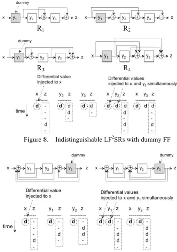
For example, consider R1 shown in Figure 7(a). R1 is a scan-testable LF2SR. The output responses for single-bit change insertion to each flip-flop are illustrated in Figure 7(b). In the figure, ‘d’ denotes a differential value or the effect of single-bit change insertion. With these responses, the LF2SR that behaves like Figure 7(b) is uniquely identified to be R1. However, if we don’t use FF y1 in R1 for normal function, i.e., there is no connection between flip-flop y1 and the kernel, no differential value can be injected to y1 from the kernel. Here, such a flip-flop is called a dummy flip-flop (shaded flip-flop in Figure 8). Note that a differential value can be injected from x at any time. Figure 8 shows four LF2SRs that are all functionally equivalent to the 3-stage shift register but their state assignments are different and hence the content of each register cannot be observed from the input/output sequence. Furthermore, as shown in the figure, the output responses of R1 obtained by single-bit change insertion are the same as those of R2, R3 and R4, and hence R1 cannot be distinguished from R2, R3 and R4 by single-bit change insertion attack, which implies the structure of R1 cannot be uniquely identified. Therefore, R1 is scan-secure, and hence R2, R3 and R4 are also scan-secure. In this way, any scan-testable LF2SR can be scan-secure by making some flip-flops dummy. Similarly, any scan-testable LFSR can be scan-secure. Figure 9 shows two indistinguishable LFSRs, where y3 is a dummy flip-flop. Figure 10 shows an example of indistinguishable pair of LF2SR and LFSR.
(a) R1
(b)
Figure 7. Effect of single-bit change insertion
R1 R2
R3 R4
Figure 8. Indistinguishable LF2SRs with dummy FF
Figure 9. Indistinguishable LFSRs with dummy FF
Figure 10. Indistinguishable LF2SR and LFSR
Theorem 8: Any scan-testable LF2SR and LFSR can be scan-secure by disconnecting some flip-flops of the ESR from the kernel, i.e., by making them dummy.
C. Cardinality of Indistinguishable Extended SRs
The cardinality of each class of k-stage I2SRs, LF2SRs and LFSR is 2k-1, 2k(k+1)/2-1, and 2k(k+1)/2-1, respectively. Although only part of these extended shift registers are scan-secure and scan-testable, there still exist many indistinguishable extended shift registers that are scan-secure.
As for I2SR, since all the L-stage I2SRs with even number of inversions are indistinguishable, the cardinality of indistinguishable k-stage I2SRs that are scan-testable and scan-secure is Θ(2k) where Θ is the notation of asymptotically tight bound.
As for LF2SR and LFSR, using the following Theorem 9 we can show that the cardinality of indistinguishable k-stage LF2SRs (LFSRs) that are scan-testable and scan-secure is Ω(2k) where Ω is the notation of asymptotic lower bound. This means the number of indistinguishable k-stage scan-testable LF2SRs (LFSRs) grows exponentially or more as k increases, and hence very high security is guaranteed.
Theorem 9: A cascade of any two extended shift registers that are scan-secure and scan-testable is also scan-secure and scan-testable. Hence, for any size k, we can easily construct an k-stage extended shift register that is scan-secure and scan-testable.
D. Area Cost and Test Power
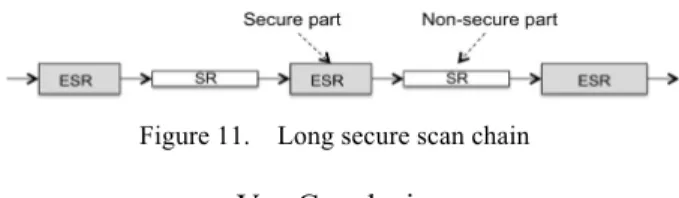
As for area cost, I2SR is superior to LF2SR and LFSR. However, I2SR is inferior to LF2SR and LFSR as to the cardinality of indistinguishable classes. To reduce the overhead due to many feed-forwards and feedbacks in a long scan chain, we can use a shift register (standard scan register) for the non-secure part that is not required to be scan-secure, as shown in Figure 11.
As for the influence on test power due to shift register modification, the insertion of inverters and/or XOR gates can reduce test power even more than standard scan design if they are inserted appropriately as shown in [12].
Figure 11. Long secure scan chain
V. Conclusions
A new secure scan design has been introduced. It involves modification of scan registers of scan design to extended scan registers. Three types have been analyzed for scan-testability and scan-security. Inversion inserted shift register can be both scan-testable and –secure by adding one extra control flip-flop. Linear feed-forward shift register and linear feedback shift register can be both scan-testable and –secure by introducing dummy flip-flop.
A long secure scan chain can be easily constructed by cascading short scan-testable and scan-secure extended shift
registers. To reduce area overhead, shift registers can be used for non-secure parts that are not required to be scan-secure. Considering the little adjustments done with scan design, the presented secure scan design requires little area overhead and no performance overhead for the normal operation. It also does not involve the use of additional keystreams. Therefore, it provides an efficient solution to satisfy both testability and security with lesser cost.
Acknowledgements
The authors would like to thank Michiko Inoue and Krishnendu Chakrabarty for their many helpful discussions. This work was supported in part by Japan Society for the Promotion of Science (JSPS) under Grants-in-Aid for Scientific Research (B) (No. 20300018).
References
[1] H. Fujiwara, Y. Nagao, T. Sasao, and K. Kinoshita, "Easily testable sequential machines with extra inputs," IEEE Trans. on Computers, Vol. C-24, No. 8, pp. 821-826, Aug. 1975.
[2] H. Fujiwara, Logic Testing and Design for Testability, The MIT Press 1985.
[3] K. Hafner, H. Ritter, T. Schwair, S. Wallstab, M. Deppermann, J. Gessner, S. Koesters, W. Moeller, and G. Sandweg, "Design and test of an integrated cryptochip," IEEE Design and Test of Computers, pp. 6-17, Dec. 1999.
[4] D. Hely, M.-L. Flottes, F. Bancel, B. Rouzeyre, and N. Berard.
"Scan design and secure chip," 10th IEEE International On-Line Testing Symposium (IOLTS’04), pp. 219–224, 2004. [5] D. Hely, F. Bancel, M.L. Flottes, and B. Rouzeyre. "Securing
scan control in crypto chips." Journal of Electronic Testing - Theory and Applications, Vol. 23, No. 5, pp. 457–464, Oct. 2007.
[6] B. Yang, K. Wu, and R. Karri. "Scan based side channel attack on dedicated hardware implementations of data encryptionstandard." International Test Conference 2004 (ITC’04), pp. 339–344, 2004.
[7] B. Yang, K. Wu, and R. Karri. "Secure scan: A design-for-test architecture for crypto chips." IEEE Trans. on Computer-Aided Design of Integrated Circuits and Systems, Vol. 25, No.10, pp. 2287–2293, Oct. 2006.
[8] J. Lee, M. Tehranipoor, and J. Plusquellic, "A low-cost solution for protecting IPs against scan-based side-channel attacks," 24th IEEE VLSI Test Symposium, pp. 94 - 99, 2006.
[9] J. Lee, M. Tehranipoor, C. Patel, and J. Plusquellic. "Securing designs against scan-based side-channel attacks." IEEE Trans. on Dependable and Secure Computing, Vol. 4, No. 4, pp. 325–336, Oct.-Dec. 2007.
[10] S. Paul, R. S. Chakraborty, and S. Bhunia. "VIm-Scan: A low overhead scan design approach for protection of secret key inscan-based secure chips." 25th IEEE VLSI Test Symposium(VTS’07), pp. 455–460, 2007.
[11] G. Sengar, D. Mukhopadhyay, and D. R. Chowdhury.
"Secured flipped scan-chain model for crypto-architecture." IEEE Trans. on Computer-Aided Design of Integrated Circuits and Systems, Vo. 26, No.11, pp. 2080-2084, November 2007. [12] O. Sinanoglu and A. Orailoglu, “Modeling scan chain
modifications for scan-in test power minimization,” International Test Conference 2003 (ITC’03), pp. 602-611, 2003.
[13] M. Inoue, T. Yoneda, M. Hasegawa, and H. Fujiwara," Partial scan approach for secret information protection," 2009 IEEE European Test Symposium, pp.143 -148, May 2009.