A Design Methodology to Realize Delay Testable Controllers
Using State Transition Information
Tsuyoshi Iwagaki Satoshi Ohtake Hideo Fujiwara Graduate School of Information Science, Nara Institute of Science and Technology
Kansai Science City 630-0192, Japan E-mail:{tsuyo-i, ohtake, fujiwara}@is.naist.jp
Abstract
This paper proposes a non-scan design scheme to en- hance delay fault testability of controllers. In this scheme, we utilize a given state transition graph (STG) to test delay faults in its synthesized controller. The original behavior of the STG is used during test application. For faults that can- not be detected by using the original behavior, we design an extra logic, called an invalid test state and transition gen- erator, to make those faults detectable. Our scheme allows achieving short test application time and at-speed testing. We show the effectiveness of our method by experiments. 1 Introduction
Modern high speed VLSI circuits require delay fault test- ing because conventional stuck-at fault testing cannot guar- antee the timing correctness of the circuits. Delay test gen- eration for such circuits is generally a hard problem. This is because there exist many sequentially untestable delay faults in a circuit [2], and the task of identifying those faults is very time-consuming. It is virtually impossible to identify all the untestable faults in a large circuit. To facilitate delay test generation, standard scan methods [7, 8] and enhanced scan ones [4, 2] have been proposed. Given a sequential circuit, these design methods make most or all of the se- quentially untestable faults detectable by making every flip- flop (FF) controllable and observable. As a result, the test generation time is significantly reduced and the fault cov- erage becomes higher. However, in scan-based delay test- ing, the test application time becomes longer because of the scan-shift operation. In addition, the scan-shift operation is generally performed at a low clock speed while the second vectors of two-pattern tests are launched at a rated clock speed. This situation may cause the IR-drop [9] because the operating speed rapidly changes, and it makes appar- ent circuit delay increase temporarily. In consequence, the test may detect temporary delay faults and it causes over- testing. Therefore, it is desirable that the operating speed is constant during test application.
Design for testability (DFT) methods at register trans- fer (RT) level have been proposed [5]. In general, an RT level circuit is composed of a controller, represented by a state transition graph (STG), and a data path, represented by hardware elements such as registers, multiplexers (MUXs) and operational modules. For delay faults, a non-scan DFT method of data paths, which overcomes the drawbacks of
scan-based testing, has been proposed [1]. On the other hand, a DFT method for stuck-at faults in controllers has been proposed [6]. This method is also non-scan based, and achieves complete fault efficiency, short test application time and at-speed testing. In this method, the above merits are realized by utilizing a given STG and by appending an extra logic, called an invalid test state generator (ISG), to the original controller.
In this paper, we propose a non-scan design scheme, which is an extension of one in [6], to enhance delay fault testability of controllers. In this scheme, we utilize a given STG to test delay faults in its synthesized controller. The original behavior of the STG is used during test applica- tion. For faults that cannot be detected by using the orig- inal behavior, we append an extra logic, called an invalid test state and transition generator (ISTG), to the original controller. In this paper, we discuss the classification of untestable faults in a controller, and show our DFT flow based on the classification. Our scheme allows achieving short test application time and at-speed testing, which is al- ways performed at a constant clock speed. Experimental results show that our method is effective in test application time compared with scan-based methods.
2 Preliminaries
2.1 Target circuit and fault model
Our target circuit is a controller represented by an STG, and we target delay faults which can be tested by two- pattern tests (e.g., transition faults and path delay faults) in the circuit. In the following discussion, we focus on the transition fault model for simplicity. Figure 1 shows an ex- ample of a controller represented by an STG. In this paper, we assume that a gate-level implementation of a controller is given, and the controller has a reset signal, i.e., we can make a transition from any state to the reset state by activat- ing the reset signal. Figure 2 shows a synthesized controller, which can be represented by a combinational circuit and a state register (SR). We also assume that, for a given con- troller, the mapping information between each state in the STG and the value of the SR (state encoding information) is available.
2.2 Terminologies
Here, we define several terminologies. For any value of the SR in a sequential circuit synthesized from a given 9th IEEE European Test Symposium (ETS'04) , pp. 168-173, May 2004.
s0
s2
s1
s3
s4
reset
Figure 1. State transition graph representing a controller.
PIs: primary inputs POs: primary outputs SR: state register R: reset signal Combinational
circuit
PIs POs
SR
R
Figure 2. Synthesized controller.
STG, the state corresponding to the value is called a valid stateif it is reachable from the reset state in the STG. Oth- erwise, it is called an invalid state. For a synthesized con- troller, a combinational circuit extracted from the controller by replacing the SR with pseudo primary inputs (PPIs) and pseudo primary outputs (PPOs) is called a combina- tional test generation model (CTGM) (Figure 3). Every two-pattern test, (V1,V2), for a CTGM can be denoted as (I1&S1, I2&S2), where I1 and I2 are the values of primary inputs (PIs), S1and S2are the values of PPIs, and “&” is the concatenation operator. A two-pattern test,(I1&S1, I2&S2), for a CTGM is said to be a valid two-pattern test if there ex- ists an arc (transition)(I, P, N, O) in a given STG such that I= I1, P= S1and N= S2, where I is an input value, P is a present state value, N is a next state value, and O is an output value. Otherwise, it is called an invalid two-pattern test. The transition corresponding to a valid two-pattern test (resp. an invalid two-pattern test) is called a valid test tran- sition(resp. an invalid test transition). For each state in- cluded in a test transition, the state is called a valid test state (resp. an invalid test state) if it is a valid state (resp. an in- valid state).
Figure 4 shows an example of test states and test transi- tions. When two-pattern tests are generated for the CTGM (Figure 3) of Figure 1, the test transitions corresponding to the generated two-pattern tests can be classified into five types:
• valid test transition (Figure 4(1)),
• invalid test transition from a valid state to a valid state (Figure 4(2)),
• invalid test transition from a valid state to an invalid state (Figure 4(3)),
• invalid test transition from an invalid state to a valid state (Figure 4(4)) and
• invalid test transition from an invalid state to an invalid state (Figure 4(5)).
3 Proposed method 3.1 Test architecture
In our testing scheme, the original behavior of a given STG is used during test application, i.e., valid two-pattern
Combinational circuit
PIs POs
PPOs PPIs
PPIs: pseudo primary inputs PPOs: pseudo primary outputs
Figure 3. Combinational test generation model (CTGM).
: invalid test transition : valid test transition
: invalid test state : valid test state s0
s2 s1
s3 s4
reset
s5
s6 (1) (2)
(3)
(5) (4)
Figure 4. Test states and transitions. tests are applied by the original behavior. The faults that cannot be detected by the original behavior are tested by an extra logic, called an invalid test state and transition gener- ator (ISTG). Our test architecture is shown in Figure 5. In Figure 5, the respective DFT elements play the following roles.
• The ISTG is used to generate invalid test states and invalid test transitions.
• The extra pin of tmodeis used to select between the nor- mal mode and the test mode.
• The extra pins of toutare used to observe the value of the SR.
• The extra pins of tselare used to distinguish among in- valid two-pattern tests1.
• The MUX is used to switch between the signal from the combinational part of the controller and that from the ISTG.
This test architecture can achieve short test application time and at-speed testing2because the scan-shift operation is never used. In our test architecture, since the ISTG is used only in the test mode, we can functionally test it during test application by observing the value of tout.
Here, we mention an impact of power consumption on a controller induced by the ISTG. Although the ISTG is only used during testing, it might consume power in the normal mode. If the impact is serious, we can avoid it by configur- ing the controller as Figure 6. In Figure 6, “AND” is used to suppress the power consumption in the ISTG during normal operation. If the value of tmodeis 1, “AND” supplies the val- ues of the PIs and the SR to the ISTG. In normal operation, the ISTG receives the constant value of zeros by setting the value of tmodeto 0. Note that, in the following discussion, we do not consider the power impact of an ISTG for sim- plicity.
3.2 Test quality
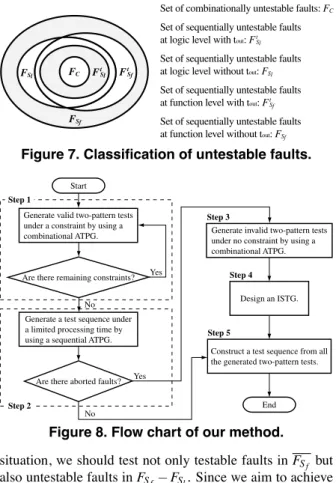
In a sequential circuit, untestable delay faults generally exist. We classify untestable delay faults in a controller into five categories in terms of “logic level”, “function level” and touthere. The classification is shown in Figure 7. All the faults in a set of FCare untestable faults in the combinational
1The details will be described in the next subsection.
2We use the terminology of “at-speed test” only if test application can always be performed at a rated clock speed.
Combinational circuit
PIs POs
tout SR
tsel
tmode 0
1
R ISTG
Figure 5. Proposed test architecture.
Combinational circuit
PIs POs
SR
R
tsel
tmode
tout
ISTG
0 1
AND
Figure 6. Power-aware configuration. part of the controller if we consider the SR as POs and PIs. These faults are called combinationally untestable faults. Some combinationally testable faults in FC are untestable because the value of the SR are restricted by the available state transitions in the synthesized controller. Such faults belong to a set of FSl (æ FC). We call these faults sequen- tially untestable faults at logic level without tout. When a given STG is synthesized, some new states and transitions are generally implemented in the synthesized controller. This implies that some testable faults in FSlare untestable if the original behavior of the given STG is only considered. We classify these faults into a set of FSf (æ FSl). These faults are called sequentially untestable faults at function level without tout. Let us consider to append tout to the synthesized controller here. Appending tout makes some untestable faults in FSl and FSf detectable. Thus, FSl and FSf change into sets of FSt
l (æ FC) and F t
Sf (æ FStl), respec-
tively.
When a sequential circuit is given, a sequential test gen- erator (ATPG) tries to identify all the untestable faults in FSland to generate tests for all the testable faults in FSl. One goal of our method is to achieve the same test quality as that targeted by a sequential ATPG. Although a fault in FSf° FSl
itself does not affect the performance of a controller under the behavior of its STG and the single fault assumption, we try to detect the fault. The reason is as follows. Suppose that there exist an untestable fault f0in FSf° FSl and a testable fault f in FSf simultaneously in a circuit, and the effect of f0 cannot be propagated to a PO but f0can be activated during normal operation. In this case, if f0is not tested, we cannot evaluate whether a test generated for f is invalidated by f0. This implies that f can be missed if there are no tests which detect f in a generated test set. In order to avoid such a
FC FtSl FSl
FSf
FtSf
Set of combinationally untestable faults: FC
Set of sequentially untestable faults at logic level with tout: FtSl Set of sequentially untestable faults at logic level without tout: FSl Set of sequentially untestable faults at function level with tout: FtSf
Set of sequentially untestable faults at function level without tout: FSf
Figure 7. Classification of untestable faults.
Generate valid two-pattern tests under a constraint by using a combinational ATPG.
Generate a test sequence under a limited processing time by using a sequential ATPG.
Generate invalid two-pattern tests under no constraint by using a combinational ATPG.
Design an ISTG.
Construct a test sequence from all the generated two-pattern tests. Are there remaining constraints?
Are there aborted faults? Start
End No
No
Yes Yes Step 1
Step 3
Step 4
Step 5
Step 2
Figure 8. Flow chart of our method. situation, we should test not only testable faults in FSf but also untestable faults in FSf° FSl. Since we aim to achieve the same test quality as that targeted by a sequential ATPG, we do not test untestable faults in FSl as much as possible although some of them are made detectable by tout. Under the single fault assumption, the above discussion does not mean anything. However, from a practical point of view, it is very useful because there can exist multiple faults in a circuit.
3.3 Flow of our method
Given a controller, the procedure of our method is per- formed as Figure 8. In the following paragraphs, we explain each step of Figure 8 in detail.
Step 1: For the CTGM of a given controller, we use a combinational ATPG. In order to generate valid two-pattern tests, we give some information (constraint) to a combi- national ATPG. A constraint is defined as a vector pair (I1C&SC1, IC2&SC2). Each bit of a constraint can take the value of 0, 1 or don’t care (X ). When we give a constraint to a combinational ATPG, the ATPG tries to generate two- pattern tests under the constraint, i.e., for every X in the constraint, a suitable value is specified.
Let us consider to use the values of transitions in a given STG as constraints. Suppose that a transition (I, P, N, O) is used as a constraint (I&P, “Xs”&N). It is obvious that two-pattern tests generated under this constraint can al- ways be applied by using the original behavior of the con- troller. Since an STG is given, we can easily extract all the constraints corresponding to the transitions with no effort.
Table 1. Truth table of an ISTG.
Inputs Outputs I11&S11 S12 I12&S21 S22
.. .
.. . I1n&Sn1 Sn2
Thus, we can obtain valid two-pattern tests. Note that, ow- ing to the presence of a delay fault f , we may fail to justify a valid two-pattern test generated for f by using the origi- nal behavior. However, it does not matter because any error induced by f in the SR can always be observed from tout. In Step 1, if we use all the constraints corresponding to the transitions in the STG, we can identify all the untestable faults in FSt
f, and valid two-pattern tests can be generated for all the faults in FSt
f. The detected faults are dropped from the fault list.
Step 2: For the remaining faults in Step 1, we try to iden- tify untestable faults in FSt
l and generate a test sequence for faults in FSt
f ° F
t
Sl by applying a sequential ATPG to the controller with tout. Since the circuit has tout, test genera- tion for it is easier than that for the original one. Moreover, the number of target faults in this step is much reduced com- pared with the total number of faults. Nevertheless, this task is very time-consuming. Therefore, we consider to use a se- quential ATPG under a limited processing time (or a limited number of backtracks) per fault. This implies that, in this step, we take into account faults which can be easily iden- tified as untestable faults and easily detectable faults. The detected faults and the untestable faults are dropped from the fault list. Notice that if there are no aborted faults in this step, we do not need to perform Steps 3 and 4. This means that only the pins of toutare added to the original controller as a DFT element.
Step 3: We generate two-pattern tests, which are invalid, for the remaining faults in Step 2 under no constraint by using a combinational ATPG. This step can identify all the untestable faults in FC.
Step 4: We design an ISTG to test the faults detected in Step 3 because we do not identify whether these faults belong to FSt
l° FC or not. An ISTG must realize func- tions to apply invalid two-pattern tests to the combinational part of the controller. Furthermore, it must also have func- tions which make all of the invalid test states in the invalid two-pattern tests reachable from the reset state. For exam- ple, given n invalid two-pattern tests t1= (I11&S11, I21&S21), t2 = (I12&S21, I22&S22), . . ., tn = (I1n&Sn1, I2n&Sn2), an ISTG need to realize the functions shown in the truth table (Ta- ble 1). Note that, in Table 1, if there exist m invalid two- pattern tests such that I11&S11= I12&S21= · · · = I1m&Sm1 and Si26= S2j(8i, j, 1 ∑ i, j ∑ m, i 6= j), we need tselto distinguish among them. The bit width of tselisdlog mmaxe, where mmax
is the maximum number of two-pattern tests that satisfy the above conditions.
We touch on a problem to reduce the area of an ISTG here. If the truth table shown in Table 1 includes X values, i.e., X values are included in two-pattern tests, we can make use of them to reduce the area of an ISTG. This problem is considered as a type of an input encoding problem [10].
Table 2. Distance matrix.
R t1 t2 · · · tn
R — d(R,t1) d(R,t2) · · · d(R,tn) t1 d(t1, R) — d(t1,t2) · · · d(t1,tn) t2 d(t2, R) d(t2,t1) — · · · d(t2,tn)
.. .
.. .
.. .
..
. . .. ... tn d(tn, R) d(tn,t1) d(tn,t2) · · · —
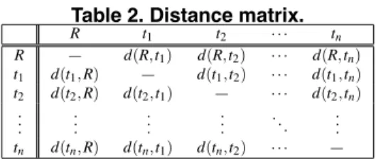
Therefore, we could apply some heuristics [10] for the in- put encoding problem to design an ISTG. However, this is still an open problem. In this paper, it is assumed that two- pattern tests generated in Step 3 do not include X values. Step 5: In order to construct a test sequence for the original circuit, we determine an order of applying all the generated two-pattern tests. Note that the test sequence generated in Step 2 is applied to the circuit before or after applying the test sequence obtained in this step. Here, we consider a problem to construct the test sequence that has the mini- mum length. It is solved as an asymmetric traveling sales- person problem (ATSP) on a complete weighted directed graph represented by a distance matrix, where a vertex t corresponds to a two-pattern test, an arc(ti,tj) corresponds to the path between tiand tj, the weight of the arc corre- sponds to the distance from ti to tj. The distance d(ti,tj) means the minimum clock cycles that are needed to apply the first vector of tj after applying ti3. Thus, we can con- struct a test sequence by solving the corresponding ATSP. Note that since it is hard to obtain the optimum solution for a large instance of ATSPs, a heuristic algorithm should be used for it. Table 2 is a distance matrix for n two-pattern tests. In this table, d(R,t) (resp. d(t, R)) denotes the mini- mum distance from the reset state R (resp. Sa) to Sb(resp. R), where Sais the reaching state after applying the second vector of t, and Sbis the state in applying the first vector of t.
4 Advantages of our method
4.1 Conventional methods and our method In this subsection, we summarize the proposed method and conventional methods (standard scan and enhanced scan ones).
Standard scan method: Test generation for a controller designed by this method requires a combinational ATPG which supports the skewed-load [7] mode and/or the broad- side [8] one. Generated two-pattern tests are applied to the controller through a scan chain in the skewed-load fash- ion and/or the broad-side one. The test application time is estimated as n(nSSFF+ 2) + nSSFF, where n and nSSFF
are the numbers of two-pattern tests and standard scan FFs (SSFFs), respectively. In this method, each SSFF in the con- troller has an additional MUX. Therefore, the area overhead is AMUX£ nSSFF, where AMUXis the area of the additional MUX. As a result, the delay of an MUX is added as the additional circuit delay. This method needs three additional pins. Note that we assume that this method has a single scan chain for simplicity.
Enhanced scan method: We can generate tests for a con- troller designed by this method by using a combinational
3If the values of the second vector of tiand the first vector of tj are identical, the value of d(ti,tj) is °1.
ATPG. The test application time is estimated as 2n(nESFF+ 1) + 2nESFF, where nESFF is the number of enhanced scan FFs (ESFFs). Each ESFF in the controller has an addi- tional MUX and a hold latch (HL) [4]. The area overhead is, therefore, (AMUX+ AHL) £ nESFF. Note that, although the area overhead can be reduced by using some techniques (e.g., [3]), we estimate it as the above equation for simplic- ity. The delay penalty is the same as that of the standard scan method because HLs themselves are not connected to the combinational part of the controller. Also, the pin over- head of this method is the same as that of the standard scan method because HLs can be controlled by the scan clock. Consequently, the total number of additional pins is 3. Note that it is also assumed that this method has a single scan chain.
Our method: In our method, we first generate tests for the combinational test generation model of a given controller by using a combinational ATPG under the constraints ex- tracted from its STG. The test generation is repeated nc
times, where nc is the number of constraints. Next, we generate a test sequence for the remaining faults under a limited processing time by using a sequential ATPG. Then, we try to generate two-pattern tests for the aborted faults in the previous step under no constraint. The test appli- cation time is determined by an order of applying all the generated two-pattern tests to the controller. The area over- head is AMUX£nFF+AISTG, where nFFis the number of FFs, and AISTGis the area of an ISTG. The proposed method has the same delay penalty compared to that of the scan-based methods because ISTGs are not used during normal oper- ation. However, in order to perform at-speed testing, we need to pay attention to the maximum delay of an ISTG. The maximum delay of an ISTG depends on its structure. In the next subsection, we evaluate the maximum delays of ISTGs by experiments. We believe that the ISTG of a given controller can be constructed with small maximum delay compared to that of the original circuit by contriving ways to synthesize the ISTG. The extra pins (tsel, toutand tmode) are needed in our method. The sum of the bit width of these pins is|tsel| + |tout| + 1. Notice that, in the proposed method, if Steps 3 and 4 are not performed, the pin overhead is|tout|. If we consider a controller-data path circuit, the PIs and the POs of the data path can be used as tseland tout, respectively. As a result of the sharing, the pin overhead decreases to 2. It is also reduced to 1 if Steps 3 and 4 are skipped.
We mention here some differences among the three methods. Since the scan-shift operation is needed in the scan-based methods, at-speed test cannot be performed, i.e., a slow clock is used except in activating delay faults. How- ever, our method can always apply tests at a rated clock speed. In this environment, the IR-drop will be suppressed. Moreover, our method can be performed flexibly accord- ing to a trade-off between hardware overhead and test gen- eration time. The trade-off is determined by the number of constraints used in Step 1 of the proposed method and by the limited processing time per fault in Step 2. In the scan-based methods, all the FFs in a circuit are modified independently of the circuit function. Consequently, most untestable delay faults in FSl° FC(Figure 7) are made de- tectable. This implies that yield loss may potentially occur. In contrast, since our method uses the original behavior of a
Table 3. Circuit characteristics.
Circuit
#PIs #POs #FFs #States #Arcs Area name
bbsse 7 7 4 16 72 295
keyb 7 2 5 19 189 459
kirkman 12 6 4 16 446 360
planet 7 19 6 48 163 937
s298 3 6 8 218 1,314 3,662
s420 19 2 5 18 155 122
sand 11 9 5 32 216 866
scf 27 56 7 121 407 1,378
given controller as much as possible during test application, many fewer untestable delay faults in FSl° FCare made de- tectable. It allows to avoid over-testing.
4.2 Experimental results
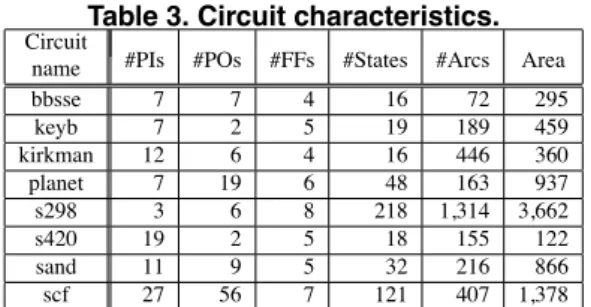
To evaluate our method, the following experiments were performed. We used the MCNC ’91 benchmark circuits shown in Table 3. A reset signal was appended to ev- ery benchmark circuit. Columns “#PIs”, “#POs”, “#FFs”,
“#States” and “#Arcs” denote the numbers of PIs, POs, FFs, states in an STG, and transitions in an STG, respectively. Column “Area” represents circuit size. The size was esti- mated by the Design Compiler (Synopsys), and the value of
“Area” was calculated by considering the area of a 2-input NAND gate to be 2. During logic synthesis, binary encod- ings were used. In the following experiments, we compared our method (NS) to the standard scan technique (SS) and the enhanced scan technique (ES). The TestGen (Synopsys) and the FlexTest (Mentor Graphics) were used as a com- binational ATPG and a sequential one respectively, and the transition fault model was targeted. Note that, in SS and ES, we assumed that the both methods have a single scan chain. For SS, we compared only the hardware overhead because the ATPGs do not support the skewed-load mode and the broad-side one.
First, we evaluate the test generation results. In this ex- periment, our method was performed as follows. Column
“#Arcs” in Table 3 corresponds to the number of constraints in Step 1 of our method. We used all the constraints in Step 1, i.e., for each circuit, test generation was repeated
#Arcs times. In Step 2, the backtrack limit was set to 64, which is not so large value. In Step 5, we used a simple algorithm to solve the ATSP and the processing time was negligibly short. Tables 4 shows the test generation results of the respective methods. Columns “TGT [s]”, “FC [%]” and “TAT [CC (clock cycles)]” denote test generation time, fault coverage and test application time, respectively. In ES, there were no aborted faults during test generation, i.e., 100% fault efficiency was achieved in all the cases. Our method encountered no aborted faults in Step 3 for all the circuits. This implies that our method also achieved 100% fault efficiency. In Table 4, the value in each parenthe- sis of column “FC [%]” (resp. “TAT [CC]”) represents fault coverage (resp. test application time) when untestable faults identified in Step 2 was removed from the fault list of ES. We listed these values to evaluate test application time fairly.
In the test generation results, the test generation time of our method was longer than that of ES because we used all the constraints in Step 1, and sequential test generation was
Table 4. Test generation results.
Circuit TGT [s] FC [%] TAT [CC]
name ES NS ES NS ES NS
bbsse 0.2 6.5 (96.29)100.00 96.29 (558)578 269 keyb 0.5 33.1 (99.00)100.00 99.00 (1,330)1,330 641 kirkman 0.4 16.6 (99.26)100.00 99.26 (908)868 514 planet 1.6 60.1 (98.18)99.96 98.18 (1,622)1,720 542 sand 2.0 33.1 (99.17)100.00 99.17 (1,714)1,762 695 s298 16.6 1,219.6 (99.90)99.97 99.90 (10,168)10,114 4,069 s420 0.1 5.8 (86.61)91.34 86.61 (298)334 156 scf 2.7 209.2 (97.92)99.84 97.92 (2,814)3,022 1,300
performed. However, we achieved low fault coverage under 100% fault efficiency compared with that of ES. This means that ES detected faults which do not need to be tested. Fur- thermore, we obtained shorter test application time. Unlike ES, we can perform at-speed test in our method. It implies that the actual test application time of our method becomes much shorter than that of ES. If it is assumed that the scan clock speed of ES is 1/5 as slow as the rated clock speed, the test application time of our method is 10 or more times faster, on average, than that of ES. Notice that, if we use one-hot encodings in logic synthesis, the advantage of our method will stand out further. This is because the test ap- plication time of ES depends on the number of ESFFs.
Next, we evaluate the hardware overhead of our method. Columns “Area OH [%]” and “Pin OH” of Table 5 denote the ratio of the area of additional hardware elements to that of the original circuit, and the number of additional test pins respectively. To calculate “Area OH [%]”, we considered areas AMUXand AHLdescribed in the previous section as 7 and 10, respectively. In Table 5, the area overhead of SS was the smallest of all. The area overhead of our method was larger than that of ES in two cases. However, our method achieved the same area overhead as that of SS in the other two cases. Note that, as mentioned in Section 3.3, if we uti- lize X values in two-pattern tests, the area overhead can be reduced. Besides, in a controller-data path circuit, the con- troller is generally much smaller than the data path. There- fore, even if the area overhead of a controller is large, it is not critical in the whole circuit. In the result of pin over- heads, our method required a large number of additional test pins for each circuit, which is shown in a parenthesis, if the sharing of test pins is not adopted. However, if the PIs (resp. POs) of the data path are used as tsel(resp. tout) in each circuit, the pin overhead can be reduced as shown in Table 5.
Finally, we mention the maximum delays of ISTGs. For every case, the maximum delay of the ISTG was smaller than that of the original circuit. This means that our method can always apply tests at a rated clock speed.
5 Conclusions and future works
This paper proposed a non-scan testing scheme to en- hance delay fault testability of controllers. In this scheme,
Table 5. Hardware overheads.
Circuit Area OH [%] Pin OH
name SS ES NS SS ES NS
bbsse 9.5 23.1 9.8 2 (3) 2 (3) 2 (5)
keyb 7.6 18.5 7.6 2 (3) 2 (3) 1 (5)
kirkman 7.8 18.9 7.8 2 (3) 2 (3) 1 (4) planet 4.5 10.9 15.6 2 (3) 2 (3) 2 (7)
s298 1.5 2.3 28.1 2 (3) 2 (3) 2 (10)
s420 28.7 111.5 45.9 2 (3) 2 (3) 1 (5)
sand 4.0 9.8 4.2 2 (3) 2 (3) 2 (6)
scf 3.6 8.6 6.6 2 (3) 2 (3) 2 (8)
the original behavior of a given STG is used during test application. For faults that cannot be detected by using the original behavior, we append an extra logic, called an invalid test state and transition generator (ISTG), to the original controller. Our scheme can achieve short test ap- plication time and at-speed testing. Experimental results showed that our method is effective compared with scan- based methods.
Our future works are to develop ways to reduce the hard- ware overhead and make the test generation under con- straints more efficient.
Acknowledgments
The authors would like to thank Prof. Michiko Inoue of Nara Institute of Science and Technology for her valu- able comments. This work was supported in part by 21st Century COE (Center of Excellence) Program “Ubiquitous Networked Media Computing” and in part by JSPS (Japan Society for the Promotion of Science) under Grants-in-Aid for Scientific Research B(2) (No. 15300018).
References
[1] Md. Altaf-Ul-Amin, S. Ohtake and H. Fujiwara, “Design for hier- archical two-pattern testability of data paths,” IEEE the 10th Asian Test Symp., pp. 11–16, 2001.
[2] T. J. Chakraborty, V. D. Agrawal and M. L. Bushnell, “Improving path delay testability of sequential circuits,” IEEE Trans. VLSI Sys- tems, Vol. 8, No. 6, pp. 736–741, Dec. 2000.
[3] K.-T. Cheng, S. Devadas and K. Keutzer, “A partial enhanced-scan approach to robust delay-fault test generation for sequential cir- cuits,”, Proc. Int. Test. Conf., pp. 403–410, 1991.
[4] B. I. Dervisoglu and G. E. Stong, “Design for testability: using scanpath techniques for path-delay test and measurement,” Proc. Int. Test Conf., pp. 365–374, 1991.
[5] M. T.-C. Lee, High-level test synthesis of digital VLSI circuits, Artech House, 1997.
[6] S. Ohtake, T. Masuzawa and H. Fujiwara, “A non-scan approach to DFT for controllers achieving 100% fault efficiency,” Journal of Electronic Testing: Theory and Applications (JETTA), Vol. 16, No. 5, pp. 553–566, Oct. 2000.
[7] J. Savir and S. Patil, “Scan-based transition test,” IEEE Trans. on CAD, Vol. 12, No. 8, pp. 1232–1241, Aug. 1993.
[8] J. Savir and S. Patil, “Broad-side delay test,” IEEE Trans. on CAD, Vol. 13, No. 8, pp. 1057–1064, Aug. 1994.
[9] J. Saxena, K. M. Butler, V. B. Jayaram and S. Kundu, “A case study of IR-drop in structured at-speed testing,” Proc. Int. Test Conf., pp. 1098–1104, 2003.
[10] T. Villa, T. Kam, R. K. Brayton and A. Sangiovanni-Vincentelli, Synthesis of finite state machines: logic optimization, Kluwer Aca- demic Publishers, 1997.
![Table 4. Test generation results. Circuit TGT [s] FC [%] TAT [CC] name ES NS ES NS ES NS bbsse 0.2 6.5 (96.29)100.00 96.29 (558)578 269 keyb 0.5 33.1 (99.00)100.00 99.00 (1,330)1,330 641 kirkman 0.4 16.6 (99.26)100.00 99.26 (908)868 514 planet 1.6 60.1 (98](https://thumb-ap.123doks.com/thumbv2/123deta/5753116.27091/6.892.479.779.167.325/table-test-generation-results-circuit-bbsse-kirkman-planet.webp)
