Acceleration of Test Generation for Sequential Circuits Using
Knowledge Obtained from Synthesis for Testability
Masato Nakazato
†, Satoshi Ohtake
†, Kewal K. Saluja
‡and Hideo Fujiwara
††
Graduate School of Information Science, Nara Institute of Science and Technology
Kansai Science City, 630–0192, Japan
‡
Electrical and Computer Engineering, University of Wisconsin - Madison
Madison, Wisconsin 53706
†E–mail:{masato-n, ohtake, fujiwara}@is.naist.jp
‡E–mail:{saluja}@engr.wisc.edu
Abstract
In this paper, we propose a method of accelerat- ing test generation for sequential circuits by using the knowledge about the availability of state justifi- cation sequences, the bound on the length of the dis- tinguishing sequence, differentiation between valid and invalid states, and the existence of a reset state. The sequential circuit is synthesized from a given FSM description by the synthesis for testability (SfT) method which takes into consideration the features of our test generation method. The SfT method guar- antees that the test generator will be able to find a state distinguishing sequence by modifying the FSM to a reduced FSM. The proposed method extracts the state justification sequence from the completely specified state transition function of the FSM pro- duced by the synthesizer to improve the performance of its test generation process. Experimental results show that the proposed method can achieve 100% fault efficiency and identify every fault to be de- tectable or redundant in relatively short test genera- tion time.
Key words:
sequential circuit, test generation, synthesis for testability, finite state machine, knowledge
1. Introduction
For general sequential circuits, it is difficult to achieve 100% fault efficiency in reasonable test gen- eration time even for single stuck-at faults. While the full scan design can convert a sequential circuit into a combinational circuit for the purpose of test gener-
ation, the cost of the full scan design is prohibitive in both area overhead and performance degradation. Therefore, an efficient sequential test generation al- gorithm is necessary which generates tests for all the detectable faults and identifies all the untestable faults in reasonable test generation time.
Most test generation algorithms for sequential cir- cuits (e.g. HITEC[2], VERITAS[3], STALLION[4] and FASTEST[5]) employ a time frame expansion model of a sequential circuit. The time frame expan- sion model is a combinational circuit that simulates the exact behavior of the sequential circuit or a given number of time frames.
HITEC is a well known sequential test genera- tor consisting of two phases. The first phase is the forward time processing phase in which a fault is activated and the resulting fault effect is propagated to a primary output. The second phase is the back- ward time processing phase which justifies the state required for activating the fault.
VERITAS test generation method is an extension of the finite state machine (FSM) verification ap- proach. This method constructs a product machine (PM) of a good FSM and its faulty version, and car- ries out reachability analysis by traversing the prod- uct machine. The information obtained by the reach- ability analysis is used to generate a test sequence. Although this simplifies generation of justification sequences, it is not as efficient as it can be because it has to deal with a much larger product machine.
In this paper, we propose a method of acceler- ating test generation for sequential circuits by us- ing the knowledge about the a set of state justifica- tion sequences, the bound on the maximum length of state distinguish sequences, the information about
IEEE 6th Workshop on RTL and High Level Testing, pp. 50-60, July 2005.
the valid states and the value of the reset state. The sequential circuit is synthesized from a given FSM by a Synthesis for Testability (SfT) method proposed in this paper which takes into consideration the fea- tures of our test generation method. The SfT method guarantees the existence of a state distinguishing se- quence of specified length by making the reduced FSM. Thus, the performance of the test generator is improved as it uses the state justification sequence extracted from the completely specified state transi- tion function of the FSM produced by the synthe- sizer. Experimental results show that the proposed method can completely identify each fault in the cir- cuit, detectable or redundant, and can achieve 100% fault efficiency in short test generation time.
The rest of this paper is organized as follows: Section 2 introduces our model and defines the ba- sic concepts. Section 3 gives the outline of the pro- posed method. Section 4 describes the proposed SfT algorithm. Section 5 describes the proposed test gen- eration algorithm for sequential circuits synthesized by our SfT algorithm. Section 6 reports the results of experiments of our method using MCNC benchmark circuits. Finally, Section 7 describes conclusions and future work.
2. Preliminaries
In this paper we consider synchronous sequen- tial circuits composed of combinational logic and D- type flip-flops (FF). All the FFs are controlled by a single clock. We assume that a reset state is defined and a reset signal is available. By applying the reset signal, both the good and the faulty circuits can be put in the reset state. We consider the single stuck-at fault model but the faults on the clock lines, inside the FFs, and on the reset lines are not included in the fault set.
This paper deals with completely and incom- pletely specified Mealy-type FSMs. An Mealy-type FSM M is defined as a 6-tupleh Σ, O, S, Sr, δ, λ i. Σ= { x0x1. . .xni,x¯0x1. . .xni,x0x¯1. . .xni, . . . ,x¯0x¯1. . .
¯
xni } is the set of the input vectors and O= { z0z1. . .zno,z¯0z1. . .zno,z0z¯1. . .zno, . . . ,z¯0z¯1. . .
¯
zno } is the set of the output vectors, where niand no
are the number of the inputs and the outputs, respec- tively. The symbols xiand zican be 0, 1orX , where X is don’t care. S = { Sr, S0, S1 , . . . , Sn ° 2 } is the set of the states, where n is the number of states and Sr is the reset state. The functions δ and λ are the next state function (δ : S £ Σ ! δ) and the output function (λ : S£ Σ ! O), respectively. We assume that all the states defined in the FSM are reachable from the reset state Sr. For example, an
Figure 1. An incompletely specified finite state machine.
incompletely specified Mealy-type FSM is shown in Figure 1.
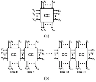
A sequential circuit Ms composed of a com- binational circuit part (CC) and FFs, is a single phase synchronous sequential circuit, where primary inputs are x1, x2, . . . , xni, primary outputs are z1, z2, . . . , zno and r is a reset input, as shown in Figure 2. We classify states represented by the FFs of Ms into valid states and invalid states as defined below.
Definition 1 (Valid State and Invalid State) A state S represented by the FFs of a sequential circuit Msis valid if S is reachable from a reset state of Ms.
Otherwise, S is invalid. 2
Definition 2 (State Distinguish Sequence) Let I be an input sequence of an FSM M. Let Oi and Oj be output response sequences of I for M with ini- tial states Siand Sj, respectively. I is called a state distinguishing sequence with respect to Si and Sj if
Oiand Ojare not identical. 2
Definition 3 (Reduced FSM) An FSM is said to be reduced if every pair of states has at least one state
distinguishing sequence. 2
The proposed test generation method employs a time frame expansion model for the test generation. Definition 4 (Time Frame) A time frame is a com- binational circuit part extracted from Msby treating its present state lines and next state lines as pseudo primary inputs( Y0,Y1, . . . ,Yq) and pseudo primary outputs( y0,y1, . . . ,yq), respectively. 2 Definition 5 (Time Frame Expansion Model) Time frame expansion model of length l for Ms is a combinational circuit which is constructed by connecting time frames such that the pseudo primary outputs of a time frame i (0 ∑ i ∑ l ° 2) is connected to the pseudo primary inputs of a time
frame i+ 1. 2
Figure 2. A sequential circuit Ms synthesized from a FSM.
(a)
(b)
Figure 3. A time frame of a sequential circuit Ms (a) and a time frame expansion model of Ms(b).
Examples of a time frame and a time frame ex- pansion model are shown in Figure 3 (a) and (b), re- spectively.
3. Outline of the Proposed Method
The proposed method consists of an SfT method and a test generation method for sequential circuits synthesized by the SfT method. The SfT method synthesizes an easily testable sequential circuit from a given FSM. The objectives of the SfT are as fol- lows.
• Any state in a sequential circuit can be identi- fied as either valid or invalid by observing an output vector from the state,
Figure 4. The flow chart of the proposed method.
• For a given k, any pair of valid states in the syn- thesized sequential circuit, which correspond to the states in the FSM, can be distinguished by a sequence of length not more than k, and
• The next state function of the FSM and that of the synthesized sequential circuit are identical. The SfT method consists of six steps shown in Figure 4.
In Step 1, for any input, we guarantee that the next states of each state defined in the FSM correspond to the states defined in the FSM. Therefore, the STG that consists of all the reachable states from the reset state of a sequential circuit and the STG that con- sists of all the states defined in an FSM are identi- cal. Notice that it is not necessary to carry out this step if the next state function of a given FSM is com- pletely specified. In this step, the output function is not changed.
In Step 2, the FSM obtained in Step 1 is modi- fied to a reduced FSM. For two states Si and Sj in the FSM obtained in Step 1, they might not be dis- tinguished by applying an input sequence of length
k or smaller to the FSM. Here, we distinguish be- tween Si and Sj by assigning values to coordinates of the output vector which have don’t care values. However, indistinguishable states, even if values are assigned to them, might still remain in the FSM. In such a case, extra outputs are added to the FSM in order to distinguish indistinguishable states and ’0’ or ’1’ is assigned to them. Hence, the reduced FSM will have at least one state distinguishing sequence of length no more than k for every pair of states.
In Step 3, we perform state assignment such that any state in a sequential circuit can be identified as either valid or invalid from the state code. This knowledge is used to identify a state as valid or in- valid for test generation method in Section 5. In or- der to realize this, continuous binary numbers are as- signed to states of the reduced FSM obtained in Step 2.
In Step 4, we further modify the reduced FSM obtained in Step 2 to distinguish between any valid state and any invalid state in the sequential circuit ob- tained after logic synthesis. In order to realize this, at most one output is added to the FSM. Different values are assigned to it for a transition from a valid state and a transition from an invalid state, respec- tively.
In Step 5, a set of state justification sequences is extracted from the reduced FSM obtained in Step 2. This is used as knowledge to accelerate the test gen- eration for sequential circuits. We will explain this in more detail in Section 4.
Finally, in Step 6, we synthesize a sequential cir- cuit with a reset input from the reduced FSM ob- tained in Step 5.
4. Synthesis for Testability
In this section, we describe the synthesis for testa- bility (SfT) method for an FSM in detail. In the method, a sequential circuit which has three char- acteristics is synthesized from an FSM. Three char- acteristics are as follows:
• An STG which consists of all the reachable states from the reset state of the sequential cir- cuit is the same as the STG which consists of all the states defined in the FSM.
• Any pair of valid states in the sequential circuit is distinguished by an input sequence of length no more than k.
• Valid states and invalid states in the sequential circuit are distinguished by an input vector.
Below, we will discuss how to synthesize a se- quential circuit with such characteristics. In order to obtain such characteristics, a given FSM is modified as follows.
• Extra outputs, if needed, are added to the FSM.
• Appropriate values are assigned to the extra outputs and to some of the coodinates which have don’t care values in the output vectors of the FSM.
4.1. Formulation of SfT Problem
We formulate the SfT problem as an optimization problem.
Input: An FSM with a reset state and the maximum length of state distinguishing sequences. Output: A gate level netlist of a sequential circuit
with a reset, a set of state justification sequences and the number of valid states.
Objective: Minimization of the number of extra outputs.
The minimization of the number of extra outputs is an NP-complete problem, because it is equivalent to the boolean SAT problem.
4.2. Synthesis for Testability Algorithm
In this section, we propose a heuristic based algo- rithm of the SfT. For a given FSM M, the following procedure is performed.
Step 1: Make the next state function completely specified
Let S be a state in M such that, there exist input vectors for which next states of the state are not spec- ified in the state transition function. For each input vector which does not have a next state, a state tran- sition from S to S (i.e., a self-loop) in M for the input vector is added to the state transition function. An output vector for the input vector is added to the out- put function. Don’t care values are assigned to every bit of the output vector. The FSM obtained in this step is referred to as Mα.
Step 2: Make the reduced FSM
To make every pair of states defined in Mαdistin- guishable, we perform two processes.
Step2.1
Let I be an input vector of the FSM Mα. Let Oi
and Oj be output response vectors of I for Mα with
Figure 5. The 2-partial successor tree. states Siand Sj, respectively. For each I, we try to distinguish between Oiand Ojas much as possible. In order to realize this, we perform two processes.
Firstly, we modify Oisuch that Oiand Ojare dis- tinguishable if Oj is covered by Oi. Here, we de- fine the relation between vectors a and b which have don’t care values. We say that a covers b if Aæ B, where A and B are the sets of values represented by aand b, respectively. Let Γ be a set of output vec- tors which are covered by Oi. If Γ6= φ , ’0’ or ’1’ is assigned to bits which have don’t care values in Oi
such that the number of elements of Γ decrease as much as possible.
Secondary, if the same output vectors which have don’t care values still exist, ’0’ or ’1’ is further as- signed to some coordinates of the same output vec- tors with don’t care values to make the output vectors different from each other. Let K be a set of the same output vectors. Let X(= x1x2. . .xi. . .xnX) be a vec- tor composed of bits which have don’t care values in κ2 K. Let nsobe the number of the same output vec- tors. The number of values represented by X is 2nX. If nso∑ 2nX, the unique value is assigned to each κ. Here, the continuous binary numbers represented by X are appropriately assigned to each κ. If nso>2nX, the value is assigned to each κ such that the num- ber of the same output vectors decrease as much as possible. Here, the continuous binary numbers are cyclically assigned to κ. The FSM obtained in this step is referred to as Mβ.
Step2.2
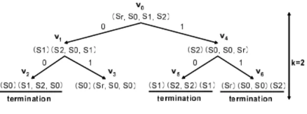
We generate the k-partial successor tree, defined below, to search whether any pair of states in Mβ could be distinguishable by applying an input se- quence of length k to Mβ.
Definition 6 (k-Partial Successor Tree) Let Sp be a set of present states in an FSM. Let gibe a group of states such that the output vectors are the same if an input vector is applied to Sp. Let Gvbe a set of all the giif an input vector is applied to Sp. A tree of depth k T= (V, E), where v 2 V is a node corresponding to Gvand e2 E is an edge corresponding to an input vector, is called a k-partial successor tree.
The tree for Mβis generated by the following pro- cedure.
The set of all the states of Mβis used as an initial set of states and it is the node of the 0thrank. When all the input vectors are applied to Gvof v of the ith rank, new nodes of the(i + 1)thrank are generated. We use the following two conditions of pruning for generation of the tree.
Condition 1: For each giof v, if all the elements of giare the same, v is a termination node. Condition 2: Let vobe a current node observed. Let
Vpbe a set of nodes such that there exists on the path from the root node to vo. If Gvp of vp2 Vpis the same as Gvo of vo, vois a termination node.
We repeat the above process until the kthrank. If the number of elements of each gi of v is one, we finish generating the k-partial successor tree.
For example, Figure 5 shows the 2-partial succes- sor tree for the FSM obtained by performing Step 1 and Step 2.1 for the FSM of Figure 1. When an input vector ’0’ is applied to the set of initial states (Sr, S0, S1, S2) refered to as v0, the next states will be either(S1) with output vector ’1’ or any of the states(S2, S0, S1) with output vector ’0’. Therefore, the reset state(Sr) and any element of the set of states(S0, S1, S2) are distinguishable. Now, we con- tinue with v1. When an input vector ’0’ is applied to Gv1 of v1 again, node v2 is generated. v2 is ter- minated by condition 2. When an input vector ’1’ is applied to Gv1 of v1, node v3is generated. Since the rank of v3 is two, v3is terminated. Continuing in this manner, when an input vector ’1’ is applied to(Sr, S0, S1, S2), node v4is generated. Node v4is not termination node because all initial states are not distinguishable and this node does not satisfy any of the conditions. When an input vector ’0’ is applied to Gv4 of v4, node v5is generated. v5is terminated by condition 1. When an input vector ’1’ is applied to Gv4 of v4, node v6is generated. v6is the same as v5. Therefore, the initial state(S2) and any element of the state set(S0, S1) are distinguishable. Hence, from the 2-partial successor tree, the indistinguish- able states are S0 and S1.
We use compatibility graph, defined below, for representing whether all the elements of the set of the initial states are distinguished.
Definition 7 (State Compatibility Graph) A undi- rected graph G= (V, E), where v 2 V is a vertex corresponding to a state of the FSM and e2 E is an edge corresponding to a pair of indistinguishable
states of the FSM, is said to be a state compatibility graph.
Some outputs are added to Mβ to distinguish all the indistinguishable state pairs. The problem to find the minimum number of additional outputs to distin- guish all the state pairs is solved as a vertex color- ing problem[7] of the state compatibility graph. The number of outputs to be added to Mβis obtained by the following formula:
na=ª log2C
|Σ| º
where C is the number of colors obtained by solving the vertex coloring problem and nais the number of the additional outputs.
Let P be a set of values represented by the addi- tional outputs. Let fibe a mapping Σ7°! P such thatfi fi6= fj,8i, j| 1 ∑ i, j ∑ C ^ i 6= j. Let vibe a vertex of state compatibility graph whose degree is more than or equal to 1. For any σ2 Σ, Mβis changed so that the value of the additional outputs become fi(σ) for the state corresponding to vi. Thus, k-state distin- guishing sequences are guaranteed for any state pair. Step3: Assign continuous binary numbers to states
Let nsbe the number of states of the FSM Mγob- tained in Step 2. The number of FF, nf f, is equal todlog2nse. The number of valid states of a sequen- tial circuit synthesized from Mγis equal to nsand the number of invalid states, niv, is equal to 2nf f°ns. Bi- nary numbers within the range of 0 to ns° 1 are used for the state assignment of the FSM and binary num- bers within the range of nsto 2nf f° 1 (if niv6= 0) are used for values of the state variables of invalid states of the sequential circuit. The value assigned to the reset state Sr is referred to as nr.
Step4: Distinguishing between valid state and in- valid state
For distinguishing between any valid state and any invalid state, one output is added to the FSM if nivis not equal to 0. For a transition from a valid state to a valid state, ’0’ is assigned to the output. For a transition from an invalid state, ’1’ is assigned to the output. The FSM obtained by this step is referred to as Mε.
Step5: Generating a set of state justification se- quence
For each reachable state from the reset state of Mε, an input sequence to reach the state from the re- set state is generated by breadth-first search method
Figure 6. The flow chart of the proposed test generation method for sequential circuits.
on the STG of Mε. For each state, the shortest input sequence is guaranteed. The input sequence is called a state justification sequence.
A set of state justification sequences for all the states of Mεis referred to as Ssi.
Step6: Synthesize
A gate level sequential circuit is synthesized from Mεby logic synthesis tools.
5. Test Generation Algorithm for Se-
quential Circuits
In this section, we describe the proposed test gen- eration method that utilizes the knowledge of a set of state justification sequences : Ssi, the maximum length of state distinguish sequences : k, the number of valid states : ns, and the value of a reset state : nr
extracted by the SfT.
Our test generation method uses a time frame ex- pansion model. A time frame expansion model has multiple faults because every time frame has a single stuck-at fault. Therefore, our test generation method uses a 9 valued logic system [8][9] for the test gen- eration to deal with multiple faults.
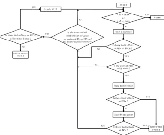
Figure 6 shows the flow chart of our test gener- ation method for sequential circuits. The proposed test generation method consists of three phases : fault excitation, state justification and fault propaga- tion.
5.1. Fault Excitation
For a target fault, fault excitation finds an ex- citation vector which is assigned to primary inputs and pseudo primary input to produce error(s) and to propagate them to the primary outputs and/or the pseudo primary output of the circuit. The pseudo primary input part of an excitation vector is referred to as an excitation state ne. The number of a valid states, ns, helps generating valid excitation vectors which are excitation vectors whose excitation states are valid states. If an excitation state is valid, the state may be justified from the reset state. However, if an excitation state is invalid, state justification is not required because the state can not be justified from the reset state. Hence, the proposed method can prune a part of search space of a test generation. This search space pruning is realized by comparing nswith ne. If neis less than or equal to ns, the ex- citation state is valid. Otherwise, the state is invalid. This feature saves a large amount of time for try- ing to generate invalid excitation vector and trying to justify the invalid excitation state. If there exists no valid state to excite the fault, the fault is proved untestable.
5.2. State Justification
Once an excitation vector is found, state justifica- tion is performed. The excitation state must be justi- fied for both the fault-free circuit and the faulty cir- cuit. We have a set of state justification sequences, Ssi, for the fault-free circuit. The fault-free state jus- tification can be easily done by choosing the state justification sequence for the excitation state from Ssi. No backtracking is required and no failures can occur in this step. The next step is to confirm if the fault-free state justification sequence is also valid for the faulty circuit. This confirmation is done by fault simulation using the fault-free state justification se- quence and observing if any invalidation occurs. An invalidation means that a state transition of the faulty circuit is different from the fault free circuit. If any invalidation occurs, the state justification sequence is invalid for the given excitation state because the state justification sequence in Ssi is not considered the invalidation under the faulty circuit. However, errors may appear to the pseudo primary outputs of an actual excitation state between the reset frame and the fault excitation frame. We try to propagate errors from the actual excitation state.
5.3. Fault Propagation
If a fault is not identified as detected or untestable by the first two phases, fault propagation is per- formed. Time frames of length k are added to the fault excitation frame. Fault propagation determines primary input values of the expanded time frames to propagate errors to a primary output. Fault propa- gation may not propagate errors to a primary output because errors may be masked by the fault within k time frames. In this case, we try to search a different excitation state by returning to the fault excitation phase. On the other hand, fault propagation may not propagate errors to the primary output but fault prop- agation may propagate errors to the pseudo primary output of the last time frame. This is because k-state distinguishing sequence is not guaranteed for faulty circuit, though the sequence is guaranteed for the fault-free circuit. Therefore, in order to make fault propagation complete, the number of time frames ex- panded from the fault excitation frame is increased 10 times (i.e., k= k £ 10) and we perform fault ex- citation again.
When the test generation time t for a fault is larger than t max or the number of the expanded time frames e is larger than e max, the proposed method aborts the generation of the fault, where t max and e maxare specified in advance.
6. Experimental Results
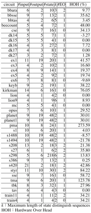
Table 1 shows characteristics of the MCNC FSM benchmarks[10] and the results of SfT. The experi- ments were performed on a SUN Blade 2000 (CPU 1GHz£ 2) with 8GB memory and a PC/AT machine (CPU Athlon 3000+) with 1GB memory. Design Compiler (Synopsys) is used as a logic synthesis tool for the Step 6 of the proposed SfT method. The num- ber of benchmarks is 53. For all the benchmarks, the proposed method could perform until Step 5. How- ever, Design Compiler was unable to perform Step 6 for 14 benchmarks because of restrictions on De- sign Compiler. All the benchmarks shown in Ta- ble 1 were synthesized by using some optimization options which optimize the area of a circuit. The first four columns give the name and the numbers of primary inputs, primary outputs and states, respec- tively. The column “k” gives the maximum length of the state distinguishing sequences. The columns
“EO” and “HOH” give the results of SfT. In this ex- periment, the maximum number of outputs added to the FSM is two: one for distinguishing between valid and invalid states and the other for making the given FSM reduced. The number of extra outputs
Table 1. Characteristics of FSM benchmarks and results of SfT.
circuit #input #output #state k #EO HOH (%)
bbara 6 2 10 3 2 9.77
bbsse 9 7 13 2 1 35.62
bbtas 4 2 6 5 1 3.45
beecount 5 4 7 2 1 48.00
cse 9 7 16 1 0 34.13
dk14 5 5 7 1 1 -3.27
dk15 5 5 4 1 0 0.00
dk16 4 3 27 2 1 7.72
dk17 4 3 8 1 0 0.00
dk27 3 2 7 2 1 1.28
ex1 11 19 20 1 1 41.57
ex3 4 2 10 2 1 16.60
ex4 8 9 14 1 1 19.37
ex5 4 2 9 2 1 19.74
ex6 7 8 8 1 0 -9.69
keyb 9 2 19 1 1 38.22
kirkman 14 6 16 1 0 76.05
lion 4 1 4 2 0 0.00
lion9 4 1 9 6 1 8.93
mc 5 5 4 1 0 0.00
opus 7 6 10 1 1 29.52
planet 9 19 48 2 1 30.01
planet1 9 19 48 2 1 30.01
pma 10 8 24 1 1 273.59
s1 10 6 20 1 1 4.03
s1488 10 19 48 2 1 -8.57
s1494 10 19 48 2 1 -21.78
s208 13 2 18 3 2 21.38
s27 6 1 6 2 2 35.80
s298 5 6 218 6 2 13.83
s386 9 7 13 2 1 0.25
s420 21 2 18 1 2 42.86
styr 11 10 30 1 2 84.22
sse 9 7 16 1 0 58.72
tma 9 6 20 1 1 123.78
tbk 8 3 32 1 1 27.96
tav 6 4 4 3 0 0.00
train11 4 1 11 2 2 34.21
train4 4 1 4 2 0 34.21
k:Maximum length of state distinguish sequences HOH:Hardware Over Head
EO : Extra Output
decreases when the FSM is reduced by only assign- ing values to the don’t cares in the output vectors of the FSM.
The average hardware overhead is 29.78%. How- ever, the hardware overhead of the circuit ’pma’ is more than 200%. It is considerable that the logic synthesis tool may not be able to simplify logic be-
cause we assign logic values to coordinates with don’t cares in input vectors and output vectors to make a given FSM reduced. However, a hardware overhead may be able to be reduced by carrying out recoding of input vectors and output vectors. Hence, still there is a room for research, how to assign cood- inates with don’t cares in input vectors or output vec- tors during SfT. The maximum time spent for the proposed SfT method is about twenty minites. For small circuits (ex. lion, bbara, bbsse, bbtas and so on), the time spent for the SfT is 0.1 second or less. Notice that since we have no way to obtain an opti- mal length of the state distinguishing sequences, we determine the maximum number by performing our SfT method within 1 hour. To find a way to do that is included in our future work.
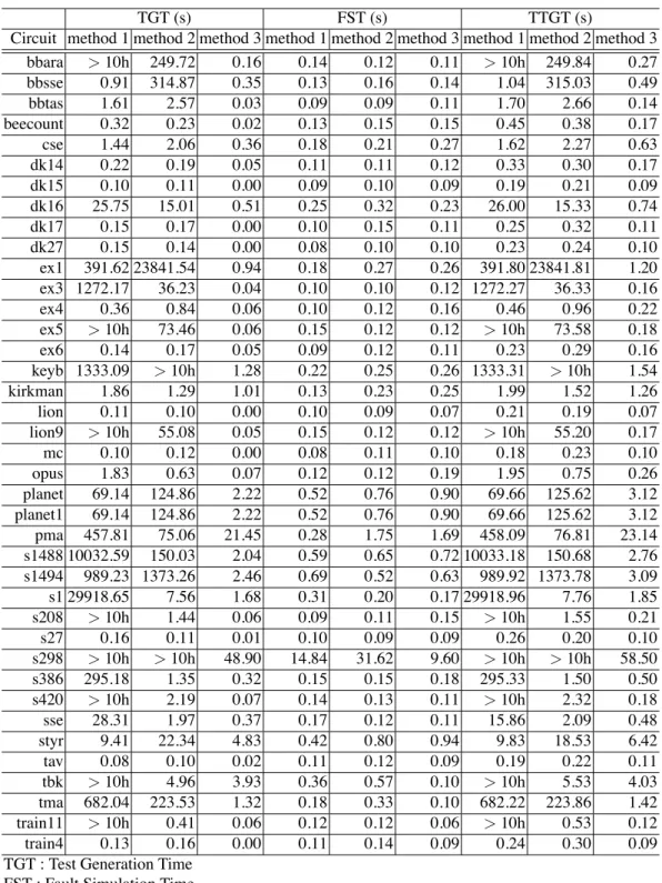
Table 2 shows the test generation time for three different methods. Method 1 applies TestGen (Syn- opsys) to the original sequential circuit synthesized from the FSM without using the proposed SfT. Method 2 applies TestGen to the sequential circuit obtained by the proposed SfT. Method 3 applies the proposed test generation method to the sequential circuit obtained by the proposed SfT. The column
“TGT (s)” is the time, in seconds, which was spent on the test generation excluding the fault simulation time. The column “FST (s)” is the time, in seconds, which was spent for the fault simulation for the test sequence obtained by the test generation. The col- umn “TTGT (s)” is the time, in seconds, which is the sum of “TGT” and “FST”. The time ’> 10h’ in the column “TGT” and “TTGT” means that the test gen- eration did not finish within 10 hours. All the meth- ods performed the equivalent fault analysis and the fault simulation which are implemented in TestGen. Since our test generator does not have the desired fault simulation capability, method 3 requires a call to the external fault simulator. Therefore, in order to compare the test generation time of the proposed method with that of TestGen on equal terms, we per- formed the fault simulation for the test sequence ob- tained by the test generation and define this fault simulation time as FST. The total test generation time for each benchmark of method 3 is shorter than that of the other methods. For some benchmarks, the total test generation time of method 2 is longer than that of method 1. However, the total test generation time for each benchmark of method 3 is shorter than that of method 2. We believe that method 3 can ef- fectively use the knowledge obtained by the SfT but method 2 can not effectively use it. The average to- tal test generation time of method 1, that of method 2 and that of method 3 are 8554.01 (s), 2531.96 (s) and
2.98 (s), respectively. The actual average total test generation time of method 1 and method 2 will be longer because these methods did not achieve 100% fault efficiency for some circuits. Method 3 identi- fied all the redundant faults within reasonable time.
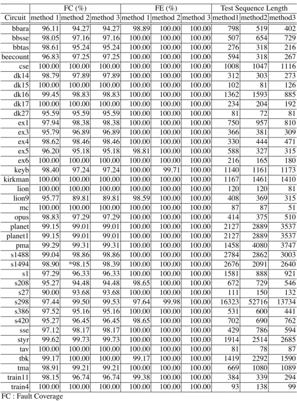
Table 3 shows the fault coverage, the fault effi- ciency and the test sequence length for three meth- ods. The column “FC (%)” is the fault coverage. The column “FE (%)” is the fault efficiency. The fault ef- ficiency is the ratio of the number of faults detected and identified redundant to the total number of faults. Method 3 can achieve 100% fault efficiency for all the benchmarks within reasonable time and shorter than method 1 and method 2. However, method 1 and method 2 did not achieve 100% fault efficiency for several benchmarks. Particularly, both method 1 and method 2 for ’s298’ did not achieve 100% fault efficiency within 10 hours. The proposed method can perform faster test generation than the conven- tional method for benchmarks.
The test sequence length of method 3 is shorter than that of method 1 for about a half of bench- marks. Moreover, the test sequence length of method 3 is also shorter than that of method 2 for about 2/3 of the menchmarks. There are some cases where the test sequence length of method 3 is longer than that of other methods, this is because TestGen uses techniques which compress the test sequence. How- ever, the average test sequence length of method 3 increases 5.27% from that of method 1 and the aver- age test sequence length of method 3 is about half of that of method 2.
7. Conclusions and Future Work
In this paper, we proposed a method for high speed test generation for sequential circuits with some specific characteristics. Such a sequential cir- cuit can be synthesized from a given FSM by the Synthesis for Testability (SfT) method which takes the features of our test generation method into con- sideration. We accelerated test generation for se- quential circuits by utilizing the knowledge that con- sisted of a set of state justification sequences,the maximum length of state distinguish sequence, the number of valid states, and the value of the reset state extracted by the SfT. The experimental results show that the proposed method can achieve 100% fault ef- ficiency in shorter test generation time compared to a state of the art test generator. Reduction of hard- ware overhead caused by the SfT method, its speed up, and further reduction of test generation time are the issues to be investigated in our future work.
Acknowledgment
Authors would like to thank Prof. Michiko In- oue, Dr. Tomokazu Yoneda, Mr. Virendra Singh and other members of Computer Design and Test Laboratory of Nara Institute Science and Technol- ogy for their valuable discussions. This work was supported in part by 21st Century COE Program and in part by Japan Society for the Promotion of Science (JSPS) under Grants-in-Aid for Scientific Research B(2)(No. 15300018), for Young Scientists (B) (No. 17700062) and in part by the grant of JSPS Research Fellowship (No. L04509).
References
[1] H. Fujiwara, Logic testing and design for testa- bility, The MIT press, Cambridge, 1985. [2] T. Niermann and J. Patel, “HITEC : A test gen-
eration package for sequential circuits,” Proc. of The European Design Automation Confer- ence, pp. 214–218, 1991.
[3] H. Cho, G. D. Hachtel and F. Somenzi, “re- dundancy identification/removal and test gen- eration for sequential circuits using implicit state enumeration,” IEEE Trans. Computer- Aided Design, vol. 12, pp. 935–945, July 1993. [4] H. K. Ma, S. Devadas, A. R. Newton and A. Sangiovanni–vincentelli, “Test generation for sequential circuit,” IEEE Trans. Computer- Aided Design, vol. 7, pp. 1081–1093, October 1988.
[5] T. P. Kelsey and K. K. Saluja, “Fast test gen- eration for sequential circuits,” Int. Conf. on Computer-Aided Design 1989, pp. 354–357, November 1989.
[6] P. Goel, “An implicit enumeration algorithm to generate tests for combinational logic circuits,” IEEE Trans. ComputerAided Design, vol. C- 30, pp. 215–222, March 1981.
[7] J. Gross and J. Yellen , Graph theory and its applications, CRC press, 1991.
[8] C. W. Cha, W. E. Donath and F. ¨Ozg¨uner, “9-v algorithm for test pattern generation of combi- national digital circuits,” IEEE Trans. Comput- ers, vol. C–27, pp. 193–200, March 1978. [9] P. Muth, “A nine-valued circuit model for test
generation,” IEEE Trans. Computers, vol. C– 25, pp. 630–636, June 1976.
[10] The CAD benchmarks at North Carolina State University, http://www.cbl.ncsu.edu/www/.
Table 2. Test generation time for each method.
TGT (s) FST (s) TTGT (s)
Circuit method 1 method 2 method 3 method 1 method 2 method 3 method 1 method 2 method 3 bbara >10h 249.72 0.16 0.14 0.12 0.11 >10h 249.84 0.27
bbsse 0.91 314.87 0.35 0.13 0.16 0.14 1.04 315.03 0.49
bbtas 1.61 2.57 0.03 0.09 0.09 0.11 1.70 2.66 0.14
beecount 0.32 0.23 0.02 0.13 0.15 0.15 0.45 0.38 0.17
cse 1.44 2.06 0.36 0.18 0.21 0.27 1.62 2.27 0.63
dk14 0.22 0.19 0.05 0.11 0.11 0.12 0.33 0.30 0.17
dk15 0.10 0.11 0.00 0.09 0.10 0.09 0.19 0.21 0.09
dk16 25.75 15.01 0.51 0.25 0.32 0.23 26.00 15.33 0.74
dk17 0.15 0.17 0.00 0.10 0.15 0.11 0.25 0.32 0.11
dk27 0.15 0.14 0.00 0.08 0.10 0.10 0.23 0.24 0.10
ex1 391.62 23841.54 0.94 0.18 0.27 0.26 391.80 23841.81 1.20
ex3 1272.17 36.23 0.04 0.10 0.10 0.12 1272.27 36.33 0.16
ex4 0.36 0.84 0.06 0.10 0.12 0.16 0.46 0.96 0.22
ex5 >10h 73.46 0.06 0.15 0.12 0.12 >10h 73.58 0.18
ex6 0.14 0.17 0.05 0.09 0.12 0.11 0.23 0.29 0.16
keyb 1333.09 >10h 1.28 0.22 0.25 0.26 1333.31 >10h 1.54
kirkman 1.86 1.29 1.01 0.13 0.23 0.25 1.99 1.52 1.26
lion 0.11 0.10 0.00 0.10 0.09 0.07 0.21 0.19 0.07
lion9 >10h 55.08 0.05 0.15 0.12 0.12 >10h 55.20 0.17
mc 0.10 0.12 0.00 0.08 0.11 0.10 0.18 0.23 0.10
opus 1.83 0.63 0.07 0.12 0.12 0.19 1.95 0.75 0.26
planet 69.14 124.86 2.22 0.52 0.76 0.90 69.66 125.62 3.12
planet1 69.14 124.86 2.22 0.52 0.76 0.90 69.66 125.62 3.12
pma 457.81 75.06 21.45 0.28 1.75 1.69 458.09 76.81 23.14
s1488 10032.59 150.03 2.04 0.59 0.65 0.72 10033.18 150.68 2.76 s1494 989.23 1373.26 2.46 0.69 0.52 0.63 989.92 1373.78 3.09
s1 29918.65 7.56 1.68 0.31 0.20 0.17 29918.96 7.76 1.85
s208 >10h 1.44 0.06 0.09 0.11 0.15 >10h 1.55 0.21
s27 0.16 0.11 0.01 0.10 0.09 0.09 0.26 0.20 0.10
s298 >10h >10h 48.90 14.84 31.62 9.60 >10h >10h 58.50
s386 295.18 1.35 0.32 0.15 0.15 0.18 295.33 1.50 0.50
s420 >10h 2.19 0.07 0.14 0.13 0.11 >10h 2.32 0.18
sse 28.31 1.97 0.37 0.17 0.12 0.11 15.86 2.09 0.48
styr 9.41 22.34 4.83 0.42 0.80 0.94 9.83 18.53 6.42
tav 0.08 0.10 0.02 0.11 0.12 0.09 0.19 0.22 0.11
tbk >10h 4.96 3.93 0.36 0.57 0.10 >10h 5.53 4.03
tma 682.04 223.53 1.32 0.18 0.33 0.10 682.22 223.86 1.42
train11 >10h 0.41 0.06 0.12 0.12 0.06 >10h 0.53 0.12
train4 0.13 0.16 0.00 0.11 0.14 0.09 0.24 0.30 0.09
TGT : Test Generation Time FST : Fault Simulation Time
TTGT : Total Test Generation Time = TGT + FST
Table 3. Fault coverage, fault efficiency and test sequence length for each method.
FC (%) FE (%) Test Sequence Length
Circuit method 1 method 2 method 3 method 1 method 2 method 3 method1 method2 method3
bbara 96.11 94.27 94.27 98.89 100.00 100.00 798 519 402
bbsse 98.05 97.16 97.16 100.00 100.00 100.00 507 654 729
bbtas 98.61 95.24 95.24 100.00 100.00 100.00 276 318 216
beecount 96.83 97.25 97.25 100.00 100.00 100.00 594 318 267
cse 100.00 100.00 100.00 100.00 100.00 100.00 1008 1047 1116
dk14 98.79 97.89 97.89 100.00 100.00 100.00 312 303 273
dk15 100.00 100.00 100.00 100.00 100.00 100.00 102 81 126
dk16 99.45 98.83 98.83 100.00 100.00 100.00 1362 1593 885
dk17 100.00 100.00 100.00 100.00 100.00 100.00 234 204 192
dk27 95.59 95.59 95.59 100.00 100.00 100.00 81 72 81
ex1 97.94 98.38 98.38 100.00 100.00 100.00 750 957 810
ex3 95.79 96.89 96.89 100.00 100.00 100.00 366 381 309
ex4 98.62 98.46 98.46 100.00 100.00 100.00 330 444 471
ex5 96.20 95.18 95.18 98.81 100.00 100.00 588 327 315
ex6 100.00 100.00 100.00 100.00 100.00 100.00 216 165 180
keyb 98.40 97.24 97.24 100.00 99.71 100.00 1140 1161 1173
kirkman 100.00 100.00 100.00 100.00 100.00 100.00 1167 1461 1410
lion 100.00 100.00 100.00 100.00 100.00 100.00 120 120 81
lion9 95.77 89.81 89.81 98.59 100.00 100.00 408 369 315
mc 100.00 100.00 100.00 100.00 100.00 100.00 87 87 51
opus 98.83 97.29 97.29 100.00 100.00 100.00 414 375 510
planet 99.15 99.01 99.01 100.00 100.00 100.00 2127 2889 3537 planet1 99.15 99.01 99.01 100.00 100.00 100.00 2127 2889 3537
pma 99.29 99.31 99.31 100.00 100.00 100.00 1458 4080 3747
s1488 99.04 98.86 98.86 100.00 100.00 100.00 2784 2862 3003 s1494 98.90 *98.15 98.39 100.00 100.00 100.00 2676 2091 2640
s1 97.29 96.33 96.33 100.00 100.00 100.00 1581 888 921
s208 95.27 94.48 94.48 98.65 100.00 100.00 672 729 546
s27 90.00 93.68 93.68 100.00 100.00 100.00 111 150 132
s298 97.44 99.50 99.53 97.64 99.98 100.00 16323 52716 13734
s386 97.52 95.16 95.16 100.00 100.00 100.00 531 600 441
s420 95.27 96.45 96.45 98.65 100.00 100.00 702 690 762
sse 97.12 98.17 98.17 100.00 100.00 100.00 429 786 594
styr 99.62 99.73 99.73 100.00 100.00 100.00 1914 2514 2685
tav 100.00 100.00 100.00 100.00 100.00 100.00 81 78 87
tbk 99.17 100.00 100.00 99.17 100.00 100.00 1419 2292 1590
tma 98.91 99.21 99.21 100.00 100.00 100.00 669 1080 1089
train11 98.15 96.74 96.74 99.38 100.00 100.00 384 339 294
train4 100.00 100.00 100.00 100.00 100.00 100.00 93 138 99
FC : Fault Coverage FE : Fault Efficiency
* : The fault coverage of all the methods is the result of TestGen. However, if the fault simulation which is implemented TestGen is performed for the test sequence obtained by TestGen after the test generation, the fault coverage is different from the result of TestGen. Hence, TestGen might potentially have some bugs.