PAPER
Design for Hierarchical Two-Pattern Testability of
Data Paths
Md. Altaf-Ul-AMIN†, Nonmember, Satoshi OHTAKE†, Regular Member, and Hideo FUJIWARA†, Fellow
SUMMARY This paper introduces the concept of hierarchi- cal testability of data paths for delay faults. A definition of hier- archically two-pattern testable (HTPT) data path is developed. Also,a design for testability (DFT) method is presented to aug- ment a data path to become an HTPT one. The DFT method incorporates a graph-based analysis of an HTPT data path and makes use of some graph algorithms. The proposed method can provide similar advantages to the enhanced scan approach at a much lower hardware overhead cost.
key words: design for testability, delay testing, hierarchical testability, two-pattern testability
1. Introduction
Two-pattern tests are necessary to detect delay defects in a circuit. The importance of detecting delay defects has soared in recent years to keep pace with the rapid increase in the speed of integrated circuits. A straight- forward solution to two-pattern testability is the en- hanced scan [1],[2]. But this incorporates very high area overhead and test application time. In the present work, we introduce hierarchical two-pattern testability of data paths. Hierarchical testability targeting stuck- at faults has been explored in a number of research works [3],[4]. These works address testability at reg- ister transfer level (RTL) and thus exploit the advan- tages of higher-level design hierarchy where the number of primitive elements in the design is greatly reduced. In these works it is shown that hierarchical testabil- ity is better than the gate-level based full-scan method in the context of test generation time, test application time and sometimes even area overhead. Our approach is hierarchical testability for delay faults. The design hierarchy we consider is RTL. At RTL a circuit can be divided into two parts: a controller and a data path. In this paper, we consider the data path only. We assume that all control inputs and status outputs of a data path are directly controllable and directly observable, respectively.
There are a number of delay fault models. Among these, the path delay fault model is more general and can overcome the limitations of other models. We de- velop HTPT data path targeting all detectable path de-
Manuscript received October 2, 2001. Manuscript revised January 21, 2002.
†The authors are with the Graduate School of Infor- mation Science, Nara Institute of Science and Technology (NAIST), Ikoma-shi, 630–0101 Japan.
lay faults. However, in the present work, we do not con- sider paths involving control inputs. The advantages of an HTPT data path are (i) the data path can be tested using any delay fault model, (ii) combinational ATPG can be used and (iii) the same fault coverage can be obtained as with the enhanced scan approach.
Analyzing the functionality of a circuit, some paths in the data path might be proven to be multiple clock tolerant paths. Delay in a multiple clock tolerant path is most likely to be caught by test for transition faults and need not be targeted for delay testing [5]. In this paper we developed our approach assuming that all paths of unity sequential depth are single clock toler- ant. However, if some multiple clock tolerant paths exist and are discarded from the target fault list, our algorithm is still applicable and may result in less hard- ware overhead. The rest of our paper is organized as follows. Section 2 discusses the RTL path and its prop- erties. Section 3 presents the definition and a graph based analysis of the HTPT data path. Section 4 ex- plains our DFT method. Section 5 shows the experi- mental results. Section 6 concludes this paper.
2. The Concept of RTL Paths
A data path consists of hardware elements and buses. We assume that the buses in a data path are of the same bit width. However, we will relax this assump- tion afterwards. The RTL paths are the paths in an RTL circuit of a data path that, (i) start at a primary input (PI) and end at a register or (ii) start at a register and end at another/same (in case of feedback) register or (iii) start at a register and end at a primary output (PO) or (iv) start at a PI and end at a PO. It is ob- vious that the sequential depth of an RTL path is one.
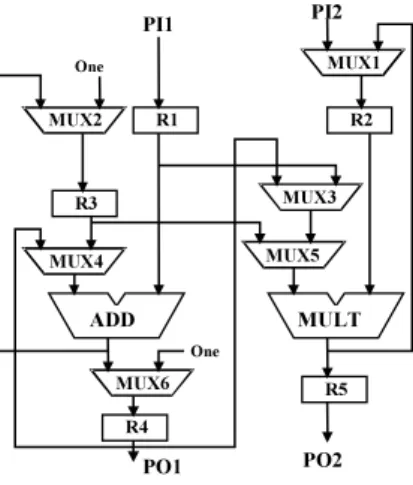
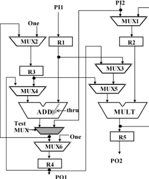
“PI1-R1” and “R1-ADD-MUX6-R4” are two examples of RTL paths in the arbitrary and simple data path of Fig. 1. We exclude the paths that start at a constant register. The reader may verify that the data path of Fig. 1 has total eighteen RTL paths.
In the lower hierarchy, each RTL path consists of a number of 1-bit wide paths. These individual 1-bit wide paths may be classified as robust, non-robust, func- tional sensitizable and functional unsensitizable paths. To guarantee the timing performance, it is necessary to test the robust, non-robust and functional sensitizable
Fig. 1 An arbitrary data path.
(FS) paths [6]. To test a robust path, it is possible to find two vectors (a vector pair) that differ from each other by only at single bit [7]. An FS path needs to be tested in a group simultaneously with one or more other FS paths. Hence the testing of a group of FS paths re- quires two vectors, which may differ from each other at multiple bits [6]. From now on the testing of an RTL path will mean the testing of the robust, non-robust and functional sensitizable paths in it.
Path delay fault testing requires launching a tran- sition at the start of a path by applying a pair of vec- tors, propagating the transition along the path and al- lowing fault effect observation from the end of the path [6]. However, many of the RTL paths in the data path neither start at a PI nor end at a PO. Therefore, some paths are necessary to ensure the flow of test data (test vectors and test responses) from PIs to appropriate reg- isters and from appropriate registers to POs. Paths used for the flow of test vectors are referred to as control paths and paths used for test responses are referred to as observation paths. Any logic value can be propagated along the control paths and the observation paths. An RTL path may cross one or more multiplexers (MUXs) and operational modules. If an input of a MUX or an operational module is on an RTL path then this input is an on-input. Other input/inputs, which are not on the path, are called off-inputs.
2.1 Paths through a MUX
In a data path, MUXs are very common elements and are used as interconnecting units. Let us consider a 2 to 1 MUX as shown in Fig. 2. Both A and B are n-bit wide. C is the control input. If C selects A then, (i) propagation of signals from A (A1, . . . ,An) to O (O1, . . . ,On) is robust (off-inputs remain stable at non-controlling value) and independent of the signals at B and (ii) there is no merging gate among the paths (A1 to O1), (A2 to O2), . . . , (An to On) i.e. there are only n mutually independent (1-bit wide) paths from
Fig. 2 n-bit wide 2 to 1 MUX.
A to O. The case for the paths from B to O is sim- ilar. Therefore, while testing any RTL path crossing one or more MUXs the select input/inputs should se- lect the on-input/inputs of the MUX/MUXs and the off-input/inputs of the MUX/MUXs can be don’t care. For example, to test the path “PI2-MUX1-R2” (Fig. 1), two-pattern vectors should be applied at P I2 and test responses should be captured at R2. The off-input of M U X1 may be don’t care.
2.2 Paths through an Operational Module
Many RTL paths cross not only MUXs but also oper- ational modules. In the following example, we discuss such a path.
Example 1: The path “R1-MUX3-MUX5-MULT- R5” in Fig. 1 crosses the operational module MULT. The segment “R1-MUX3-MUX5-” of this path is like a wire in a sense that the signal values at R1 appear unchanged at the output of the M U X5 if the control inputs of the MUXs select the on-inputs. Again the segment “-R5” on the output side of MULT is obvi- ously like a wire. The core segment of this path is the part of the path inside the MULT. In other words the test vector set required to test the part of the path in- side the MULT is the same as to test the whole path
“R1-MUX3-MUX5-MULT-R5.” These test vectors can be generated by separately considering the gate level circuit structure of the MULT. Obviously the bit width of these test vectors spans both inputs of the MULT. Suppose bits of the test vectors to be applied to the off- input of the MULT are not all don’t cares. Hence to test the path “R1-MUX3-MUX5-MULT-R5,” test vec- tors should be applied not only at R1 but also at the off-input of the MULT. Test vectors can be applied at the off-input of the MULT from register R2. Therefore, we say that the RTL path “R1-MUX3-MUX5-MULT- R5” is an HTPT path if, (i) there exist two control paths from PI/PIs to R1 and R2 that support the ap- plication of two-pattern vectors and (ii) there exists an observation path to propagate the test responses from R5 to a PO.
In Fig. 1, we can see that disjoint control paths
“PI1-R1” and “PI2-MUX1-R2” are sufficient to apply
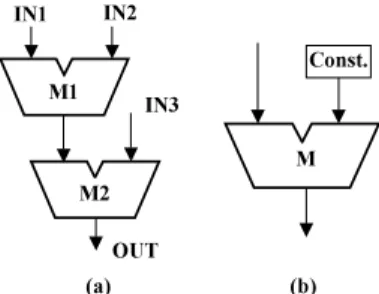
Fig. 3 (a) Chaining of modules,(b) A module connected to a constant register.
two-pattern vectors and the test response can be ob- served using the observation path “R5-PO2.” It is no- ticeable that these control and observation paths can also test the RTL path “R2-MULT-R5.” ✷ Though most of the operational modules com- monly used in data paths have two inputs, there might be cases of chaining as shown in Fig. 3 (a). This type of module can be regarded as a 3-input operational mod- ule. Based on the similar reasons explained in Exam- ple 1 it can be realized that three control paths and only one observation path would be sufficient to test any RTL path that crosses such a module. Some mod- ules in a data path may have their inputs connected to constant registers. If x inputs of an m-input op- erational module (x < m) are directly connected to constant registers then we regard such a module as an (m − x)-input operational module. The module M of Fig. 3 (b) is considered as a 1-input module.
3. The HTPT Data Path
In this section we define the HTPT data path and some other related terms. In the following subsections we present an analysis on HTPT data paths.
Definition 1: The degree of an RTL path is n, if it crosses an n-input operational module.
For example, the path “R1-MUX3-MUX5-MULT- R5” of Example 1 is an RTL path of degree 2. There might be paths in a data path that crosse no oper- ational module. In Fig. 1, the path “PI2-MUX1-R2” crosses only a MUX and the path “PI1-R1” is simply a wire. These paths are considered as RTL paths of de- gree 1. The degree of an RTL path implies the number of control paths that are sufficient to ensure its hierar- chical two-pattern testability.
Definition 2: An RTL path of degree n, which crosses an n-input operational module say M is an HTPT path if there exist n control paths C1, C2, . . . ,Cn and an observation path P1 such that, (i) C1 is from a PI to the starting register of the path (in the case that it starts at a PI, C1 is an empty path) and (ii) C2. . .Cn is from PI/PIs to a register/registers which are either directly or through MUX/MUXs con- nected to the n − 1 off-input/inputs of M (in the case
that an off-input of M is connected to a PI, the corre- sponding control path is an empty path) and (iii) C1, C2, . . . ,Cn support the application of two-pattern test and (iv) P1 is from the ending register of the path to a PO (in the case that the path ends at a PO, P1 is an empty path).
Definition 3: The set of control paths and an obser- vation path that are sufficient to ensure the hierarchical two-pattern testability of an RTL path is referred to as the test plan of the path.
Definition 4: A data path is an HTPT data path if each of its RTL paths has a test plan.
3.1 Conditions for Control Paths to Support Two- Pattern Test
Here, we first briefly discuss the thru function [3]. The thru function allows the propagation of a logic value from an input to the output of an operational mod- ule without any change. For common two-input oper- ational modules (e.g. adder, multiplier, etc.), a thru function from an input to the output can be realized by providing a constant at the other input. The nec- essary constant can be provided either by means of a support path or by adding a mask. For other modules thru functions can be realized by a MUX. Initially, we assume that a thru function exists from any input to the output of any operational module. Under this as- sumption, a control path can be represented by lines and the registers it crosses. However, such an assump- tion is not necessary for an HTPT data path and will be relaxed later on.
The general condition: Let C1, C2, . . . ,Cn are n control paths starting at PI/PIs and ending at n dif- ferent points EP1, EP2, . . . , EPn (these ending points may be either registers or PIs). Let, a vector pair (v1, v2) span over n control paths. Hence each of v1and v2
can be divided into n partial vectors. Each of the par- tial vectors is associated with a control path. Based on this, we represent v1 and v2 as v1 = v11&v12&. . . v1n
and v2 = v21&v22&. . . v2n (the symbol ‘&’ merely links the partial vectors). Bit-width of each of v11, v12, . . .v1n, v21, v22, . . .v2n is equal to the bit-width of the data path. Let v11, v12, . . .v1n, v21, v22, . . .v2n
can be fed from PI/PIs according to a schedule such that v11, v12, . . .v1n simultaneously appears at EP1, EP2,. . . EPn and in the next clock cycle v21, v22, . . .v2n simultaneously appear at EP1, EP2,. . . EPn then we say that C1, C2. . .Cn support the application of two-
pattern test. ✷
The sequential depth of a control path is the num- ber of registers that appear on the path. To denote the sequential depth of any control path say, C1we use the notation SD(C1). In the following theorem we men- tion necessary and sufficient conditions for two control paths to support two-pattern test.
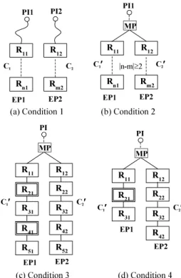
Fig. 4 Control paths depicting the conditions of Theorem 1.
Theorem 1: Two control paths C1 and C2 from PI/PIs to two different points EP1 and EP2 support the application of two-pattern test if and only if one of the following conditions is satisfied:
Condition 1: C1∩C2= φ i.e. C1and C2are disjoint. Condition 2: |SD(C′1) – SD(C′2)| ≥ 2, where C′1 and C′2 are disjoint parts of C1 and C2 from EP1 and EP2 respectively to the nearest merging point of C1and C2. Condition 3: Either C′1 or C′2 crosses at least two hold registers.
Condition 4: When |SD(C′1) – SD(C′2)| = 1, the dis- joint part (i.e. one of C′1 or C′2) with lower sequential depth crosses a hold register.
Proof: An arbitrary vector pair (v1, v2) involving two control paths can be represented as v1= v11&v12 and v2 = v21&v22. In the following the sufficiency and the necessity of the above four conditions are discussed. Sufficiency:
Condition 1: In Fig. 4 (a), m and n are two arbitrary numbers. Hence it represents a general topology that matches with Condition 1. Here, v11and v21can be fed from PI1 in consecutive clocks and similarly v12and v22
can be fed from PI2. The general condition can be met by differing the feeding from PI1 and PI2 by |m − n| clocks.
Condition 2: In Fig. 4 (b), m and n are two arbitrary numbers such that |n − m| ≥ 2. Hence it represents a general topology that matches with Condition 2. All
Table 1 Schedule of partial vectors corresponding to Fig. 4 (c).
partial vectors should enter C′1 and C′2 clock by clock through the merging point MP. Hence any other merg- ing between C1 and C2 before MP has no effect. Let n > mand n − m = r. Therefore according to Condi- tion 2, r ≥ 2. The general condition can be met by first allowing v11 and v21 to enter C′1 in consecutive clocks and then after r − 2 clocks by allowing v12 and v22 to enter C′2in consecutive clocks.
Condition 3: Any of C′1 and C′2, say C′1 crosses two hold registers. First allowing v11 and v21 to enter C′1
and then allowing v12 and v22 to enter C′2 the general condition can be met. Here, v11 and v21 might be re- quired to hold for one or more clock cycles in the hold registers of C′1 depending on the position of the hold registers and the number of registers in C′1 and C′2. An example that matches with this condition is shown in Fig. 4 (c) and the corresponding scheduling of the ap- plication of the partial vectors is shown in Table 1. In Fig. 4, registers with double line border are hold regis- ters. Referring to Table 1, v11and v21are fed to C′1in the 1st and 2nd clock and v12 and v22are fed to C′2in the 3rd and 4th clock. Notice that v11 and v12 simul- taneously appear at EP1 and EP2 in the 7th clock and v21 and v22 do the same in the following clock. The contents of the registers for certain clocks that are not important to this scheduling are not shown in the table. Condition 4: Any of C′1 and C′2 say C′1 crosses a hold register and so according to Condition 4, SD(C′2) – SD(C′1) = 1. Now, first allowing v11 to enter C′1 and then immediately allowing v12and v22 to C′2 and then again allowing v21 to C′1 the general condition can be met. An example that matches with this condition is shown in Fig. 4 (d) and the corresponding scheduling of the application of the partial vectors is shown in Ta- ble 2. The explanation of Table 2 is similar to that of the Table 1.
Necessity:
Two control paths C1 and C2that do not fulfill any of the above four conditions should satisfy all the following properties.
Table 2 Schedule of partial vectors corresponding to Fig. 4 (d).
1. C1 and C2are not disjoint. 2. |SD(C′1) – SD(C′2)| = 0 or 1.
3. None of C′1 or C′2crosses two hold registers. 4. When |SD(C′1) – SD(C′2)| = 1, the disjoint part (i.e. one of C′1 or C′2) with lower sequential depth does not cross a hold register.
All possible cases fulfilling the above properties are as follows.
1. C1 and C2 are not disjoint and |SD(C′1) – SD(C′2)| = 1 or 0 but none of C′1 and C′2 crosses any hold register.
2. C1 and C2 are not disjoint and |SD(C′1) – SD(C′2)| = 0 and any one or both of C′1 and C′2 crosses a hold register.
3. C1 and C2 are not disjoint and |SD(C′1) – SD(C′2)| = 1 and the disjoint part with higher sequen- tial depth crosses a hold register.
However, no scheduling can obviously be found for these cases to fulfill the general condition. Hence Con- dition 1, Condition 2, Condition 3 and Condition 4 are the only conditions for two control paths to support the
two-pattern test. ✷
In general case, any number, say n control paths can merge in numerous fashions. Each of these fash- ions may be of different nature depending on the num- ber and position of hold registers in each control path. Hence to find out necessary and sufficient conditions for ncontrol paths to support two-pattern test is a complex task. However in the following theorem some sufficient conditions are mentioned
Theorem 2: ncontrol paths support the application of two-pattern test if one of the following conditions is satisfied:
1. All n paths are disjoint
2. Mutually disjoint parts of n − 1 paths from their end points cross two hold registers.
3. The merging fashion of n paths after MP is a tree with MP as the root and the difference of sequential depths of any two partial paths from MP to their re- spective end points is two or more, where MP is the nearest merging point of all n paths from their end points.
Proof: The proof of this theorem is similar to that of
Theorem 1. ✷
Here, one thing is noteworthy. Let an RTL path P start at a register R and crosses an operational module M. For P to be an HTPT path, a control path from a PI to R is necessary. Now, if R is a feedback regis- ter (FR) to M, the control path must not incorporate a thru function to M. In Fig. 1, R3 is an FR to ADD. Only one control path from a PI to R3 is “PI1-R1-ADD- MUX2-R3.” This control path cannot be used to test the path “R3-MUX4-ADD-MUX6-R4.” It cannot be used because the first vector of a vector pair is loaded at R3 to settle the signal lines throughout the path in- cluding the part of the path in ADD. In the next clock, the second vector is loaded at R3 to launch the desired transition. However, the first vector cannot do its job if the second vector propagates using a thru function to ADD. Therefore, we should always carefully exclude such control paths.
3.2 Graph Based Analysis of HTPT Data Paths All RTL paths that cross an operational module having two or more inputs can be represented as a graph. We call this graph the structural connectivity graph (SCG) of the module. The nodes of the SCG consist of the module and the registers, PIs and POs that are at the starting and at the ending of the RTL paths through the module. The edges of the SCG represent the con- nections of the module with the other nodes. Let the set of nodes connected to each of the inputs of an n- input module be Ri1, Ri2,. . . Rin and the set of nodes connected to the output of the module is Ro. Let Ri1
= {r11, r21, r31 . . . }, Ri2 = {r12, r22, r32 . . . },. . . Rin
= {r1n, r2n, r3n . . . } and Ro= {r1, r2, r3 . . . }. From the SCG of an n-input module an (n + 1)-partite graph can be generated. We call this the register compatibil- ity graph (RCG) of the module. Ri1, Ri2,. . . Rin and Ro are the n + 1 set of nodes. The edges of the RCG are determined by the following rules.
Rule 1: If there exist n control paths C1, C2. . .Cn
from PI/PIs to any node rj1∈Ri1, rk2∈Ri2,. . . rln∈ Rin, that support the application of two-pattern test, there exist edges between any two nodes of rj1, rk2, . . . and rln.
Rule 2: If there exists an observation path from any node rm ∈ Ro to a primary output, there exist edges between rmto any node in Ri1 and Ri2,and . . . Rin. Example 2: The SCG of MULT of Fig. 1 is shown in Fig. 5 (a). Figure 5 (b) shows the RCG of MULT gener- ated under the assumption that a thru function exists from any input to the output of any operational mod- ule. Table 3 shows that which edge/edges in Fig. 5 (b) are related to which control or observation path/paths.
✷
Fig. 5 (a) SCG and (b) RCG of M U LT of Fig. 1.
Table 3 List of edges of the graph in Fig. 5 (b) and correspond- ing paths.
Definition 5: An edge in the RCG of a module from any node in Roto any node in Ri1or Ri2,. . .orRin, ac- tually represents an RTL path through the module and hence we refer to such an edge as a path edge.
Definition 6: An edge in the RCG between any two nodes of Ri1,Ri2,. . .andRinis a control edge.
Definition 7: If a sub-graph of the RCG of a module with only one node from each of Ri1, Ri2,. . . Rin and Ro is a clique, then this is referred to as a test clique. A test clique implies the existence of n control paths and one observation path, which are sufficient to test nRTL paths passing through n inputs of the module, i.e. a test clique in the RCG of an n-input module incorporates test plan for n paths.
Theorem 3: All RTL paths through a module are two-pattern testable if the path edges corresponding to all RTL paths through the module exist in its RCG and each path edge is part of some test clique.
Proof: If a path edge is part of a test clique, then this test clique is sufficient to guarantee the two-pattern testability of the corresponding path. Now if each path edge is part of some test clique, then each RTL path passing through the module is two-pattern testable.
✷ 4. Details of the DFT Method
This section discusses the DFT elements we utilize in our approach and also the algorithm for efficient addi- tion of the DFT elements to augment a data path to an HTPT one.
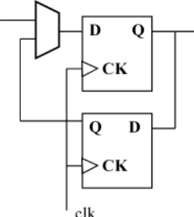
Fig. 6 Rotating enhanced flip-flop.
4.1 The DFT Elements
We consider three types of DFT elements in our ap- proach. They are MUXs, thru functions and rotating enhanced flip-flops (REFFs). The operation of a MUX is well known. We briefly explained about the thru function in Sect. 3.1. An REFF consists of two flip- flops and a MUX as shown in Fig. 6. The control input of the MUX is used as the mode selector. In normal mode the REFF behaves like a normal flip-flop. Using normal mode two bits can be loaded to the REFF. Just after loading two bits, the mode can be changed to test mode. In test mode the bits exchange their position at every clock but remain stored in the REFF. Hence an REFF can be regarded as a 2-bit hold register. Of a two-pattern vector, the bit of which vector should be loaded first to the REFF depends on the time of loading and the time of applying the vectors.
4.2 Algorithm for Adding DFT Elements
Figure 7 illustrates the flowchart of our algorithm. In the following subsections we describe in detail the tech- niques and heuristics we use for different steps of the flowchart. For simplicity we describe our algorithm as- suming that operational modules in the data path has a maximum two inputs and there is no chaining of mod- ules. This means there is no RTL path of degree 3 or more in the data path. Most of the benchmarks satisfy this condition. Also, our approach can be extended for data paths with modules having more than two inputs. 4.2.1 Selecting Potential Control and Observation
Paths
Every register (other than the constant registers) of a data path is at the starting of some RTL path and also at the ending of some RTL path. Control paths are therefore necessary from PIs to all registers and so are the observation paths from all registers to POs. How- ever the number of paths in the data path can be very large and we use some heuristics to select some poten- tial control and observation paths. We make a set CP of potential control paths and a set OP of potential
Fig. 7 Flow-chart of the algorithm.
observation paths for each register R. The first mem- bers of CP are the shortest depth paths from each PI to R. We favor the shortest depth paths because they help to reduce the test application time. To determine the shortest depth control paths, we represent the data path as a port digraph [8]. The digraph of the data path of Fig. 1 is shown in Fig. 8 (a). A node represents a port in the data path and any edge say, (u, v) im- plies that either a metal line connects u to v or u and v are input port and output port, respectively of the same element. The shortest depth control paths can be selected by performing a modified breadth first search (BFS) on the digraph. The BFS is performed n times where n is the number of PIs of the data path. Each of n PIs are once considered as the source node. Fig- ure 8 (b) shows the breadth first tree (thick lines) of the digraph of Fig. 8 (a) considering PI1 as the source node. This tree contains the shortest depth paths from PI1 to each register reachable from PI1. Similarly the members of OP of any register R are the shortest depth paths from R to each PO. The shortest depth observa- tion paths can be determined by reversing the edges of the digraph and performing similar BFS m times where m is the number of POs. For each member of CP and OP of each register we maintain a variable, which we refer to as the “cost” of the path. The cost of the path is nothing but the number of thru functions associated with the path, i.e. the cost of a thru function is 1.
Fig. 8 (a) Port digraph of the data path of Fig.1,(b) Breadth first tree of the digraph of fig.8(a).
4.2.2 Adding Direct Paths to Feedback Registers We first consider the FRs of all modules. Suppose a register Rf appears on both input and output sides of the SCG of a module M. This implies that Rf is an FR to M. Now, if a control path from a PI to Rf
incorporates a thru function to M, then this control path cannot be used to test any RTL path that crosses M (explained in Sect. 3.1). So we first find in the CP of Rf for a control path without a thru function to M. If we succeed, we switch to another FR of M or FR of other module. If no such control path is found in the CP of Rf we search the entire data path. For this search, we remove the edges from inputs to output of M in the digraph and then find shortest path from each PI to Rf until a path is found. If a path is found, this path is added to the CP of Rf. However the failure of such a search implies that there is no control path from any PI to Rf without a thru function to M. Under such a situation a direct path is added to Rf using a test MUX from a PI. This PI is chosen based on the control paths in CPs of the registers connected to the other input of M (input to which Rf is not connected). If the majority of the nodes connected to the other input of M have control path from a PI, we choose other PI for Rf. This direct path is included to the CP of Rf. In case the data path has single input, it might be difficult to find a suitable PI. In such a situation we augment each flip-flop of Rf to REFF. This information is added to the paths in the CP of Rf. We then switch to another FR of M or FR of another module until all FRs in the data path are considered. We start to consider the FRs of the modules nearer to PIs first. Sometimes a single MUX can be used for more than one FR of a module. In Fig. 9, the test MUX is providing control paths from P I2 to both R3 and R4. In the case of a single input Data path, if it becomes necessary to augment flip-flops of more than one register to REFF, we use a global
Fig. 9 The HTPT equivalent of the data path of Fig. 1.
REFF register connected to the only PI of the data path. Such an REFF register can be used as a PI for two-pattern testing. This is because an REFF can store two bits for as long as it is necessary. Direct paths then can be added from the global REFF register to FRs using test MUXs. We use global REFF because the hardware overhead incurred by registers is very high. Whenever we add any DFT element, we update the CPs of registers affected by the addition. Addition of test MUXs and REFF registers creates some more paths of degree 1 in the data path. We should also consider the two-pattern testability of these paths. Because of adding DFT elements in this step, the SCGs of modules in the data path remain unchanged.
4.2.3 Determining Test Plans
We discussed our algorithm for adding some DFT ele- ments in the previous section. In this section, we add more DFT elements to ensure the test plans for all RTL paths. First we address the RTL paths of degree 2 and then of degree 1.
RTL paths of degree 2: We consider all RTL paths passing through a module at a time. The following four steps are performed for each 2-input operational module.
Generating RCG from SCG (step 1): Let M be a 2- input module and Ri1, Ri2 and Roare the set of nodes connected to the left input, right input and output of the module. Each member of Ri1 and Ri2 has a set of control paths CP and each member of Ro has a set of observation path OP. Let rj1∈Ri1 and rk2∈Ri2. Now we look for two control paths, one from CP of rj1 and other from CP of rk2, such that they satisfy any one of the four conditions of Theorem 1. In case we find more than one pair of control paths to satisfy any condition of Theorem 1, we choose the pair having lowest cost.
We add a control edge between rj1and rk2in the RCG and keep a record of the lowest cost control paths that support this edge. We should keep in mind that in the case that rj1and rk2is a FR to M, we cannot consider a control path for rj1or rk2 incorporating a thru function to M unless rilor rjris augmented to an REFF register. If we fail to find a control edge between rj1 and rk2 we switch to another pair of nodes. We search for control edges between every possible pair of nodes with one node from Ri1and one node from Ri2. For each member of Ro, we choose the lowest cost observation path from its OP and add path edges to the RCG as described in rule 2 in Sect. 3.2.
Adding DFT elements to Augment RCG (step 2): In the RCG, some node/nodes of Ri1 or Ri2 may not be connected to any control edge. For any such node we add DFT elements to create a control edge in the RCG incorporating this node. First we try by adding a direct path to such a node from some PI by means of a test MUX. In the worst case we augment such a node to an REFF register. However, if it becomes necessary to augment more than one register, we create a global REFF register as mentioned in Sect. 4.2.2. Direct paths can then be created from the global REFF register to the required nodes by means of test MUXs. The RCG of M is now sufficient for two-pattern testability of any RTL path through it. However, when a direct path to a node is created, we check whether this path can be utilized to remove some DFT elements added for the previously processed modules. A direct path to a node might be used instead of some other necessary control path/paths to the same node, which incorporates a thru function.
Minimizing control edges in RCG (step 3): The RCG may have some excess control edges. Of all the control edges we select the minimum number of them that fulfill the condition that each node in Ri1 or Ri2is connected to at least one control edge. The minimum number of control edges will create the minimum number of test cliques in the RCG that are sufficient for test plans of RTL paths through M.
Adding DFT elements for thru Functions (step 4): At this step, we relax the assumption that a thru function exists from any input to the output of any operational module. We first check whether a thru function that we need really exists (can be implemented by a sup- port path) or whether we should add a DFT element (mask or others) for it. To do this we consider one test clique at a time. A test clique in the RCG of a two-input operational module incorporates two control paths and one observation path. We search for sup- port paths for the thru functions associated to these three paths using some manual calculation. A support path may have a timing conflict with control paths or other support paths. Timing conflict means it becomes necessary to provide different values at the same PI at the same time. We add mask elements to realize the
thru functions for which any support path cannot be found without timing conflict. The cost of the thru function realized by a mask element becomes zero and we update the cost of all control and observation paths, which includes this thru function. We consider all the test cliques in the RCG of M in a similar way.
The above four steps are performed for all 2-input modules considering the modules nearer to the PIs first. When we finish all the 2-input modules, the testability of all the RTL paths of degree 2 is ensured.
RTL paths of degree 1: We now consider the testabil- ity of RTL paths of degree 1. Let Rs and Re be the start and end registers of an RTL path of degree 1. We choose the lowest cost path from the CP of Rs as the control path and the lowest cost path from the OP of Reas the observation path. If any thru function of cost 1 is associated with these paths, we try to realize it us- ing a support path. In case we cannot find any support path without timing conflict, we add a mask element or a multiplexer to realize them. We consider all RTL paths of degree 1 in a similar way. Figure 9 shows the HTPT equivalent of the data path of Fig. 1 augmented by following the algorithm described above.
4.3 Relaxing the Assumption of Bit Width
In practice, a data path may not be of consistent bit width. It is not a problem, if a control path becomes gradually narrower or an observation path becomes gradually wider in their respective downstream. How- ever, in the case of a control path, it is a problem if it is narrower than its end point anywhere in the up- stream. Such a problem can be tackled by means of a MUX or an REFF and a MUX. In the case of an ob- servation path, it is a problem if it becomes narrower than its start point anywhere in the downstream. Such a problem can be tackled by using one or more MUXs. 5. Experimental Results
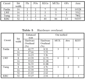
In this section we present experimental results to com- pare our method with the enhanced scan approach. For comparing area overhead we applied our method to data paths of three benchmark circuits and a RISC processor provided by industry. The characteristics of these data paths are shown in Table 4. In this table PIs and POs denote the number of primary inputs and primary outputs of the data path respectively. REGs, MUXs and OPs are the numbers of registers, multiplex- ers and operational modules in the data path. The last column of Table 4 shows the areas of the data paths generated by the logic synthesis tool Design Compiler (Synopsys).
Table 5 shows the results regarding hardware over- head. In both our method and the enhanced scan ap- proach, the percentage of area overhead decreases with the increase in bit width of the data paths. However,
Table 4 Circuit characteristics.
Table 5 Hardware overhead.
Table 6 Test application time for 100% coverage of robust and non-robust testable paths (cycles).
the area overhead incurred by our method is always much lower. For our DFT method, the columns MUX, thru and REFF show the number of added MUXs, thru functions and REFF registers.
The tool we used for the experiments to compare test application time are DelayPath and TestGen from Synopsys. DelayPath can generate path list for designs of up to 5000 gates. And TestGen can generate tests for only robust and nonrobust testable paths. Because of these limitations we conducted our experiments for the data path of Paulin, LWF and Tseng considering their bit width only 8. Also, test vectors that cover only robust and non-robust testable paths are consid- ered. 100% coverage is obtained for robust and non- robust testable paths in both our method and the en- hanced scan approach. Identifying and generating tests for functional sensitizable paths in a large multi-level circuit is a hard task [6]. However, if test can be gener- ated for such paths, both our method and the enhanced scan approach allow their application.
Table 6 shows the results of our experiments re- garding test application time. For all three data paths the test application time of our method is much shorter compared to that of the enhanced scan approach. This is because, in the enhanced scan approach, the test vec- tors and test responses are shifted in to and shifted out from the enhanced scan chain serially. Contrary to this our method supports the parallel propagation of test
vectors and test responses via data path lines. 6. Conclusions
The concept of hierarchical testability for delay faults is introduced in this paper. Precomputed vector pairs are propagated via control paths from primary inputs to appropriate locations and are applied in a two-pattern fashion to test paths of unity sequential depth. Test responses are propagated via observation paths from the end points of paths under test to primary outputs. A DFT method is also presented that can be applied to augment a data path to become a hierarchically two- pattern testable one. Priority has been given to use the existing paths in the data path as control paths and observation paths. Experimental results show that the area overhead and test application time of our DFT method is smaller compared to those of the enhanced scan approach for some benchmark data paths. Acknowledgments
This work was sponsored in part by NEDO (New En- ergy and Industrial Technology Development Organiza- tion) through the contract with STARC (Semiconduc- tor Technology Academic Research Center) and sup- ported by Japan Society for the Promotion of Science (JSPS) under the Grant-in-Aid for Scientific Research and by Foundation of Nara Institute of Science and Technology under the grant for activity of education and research.
References
[1] B.I. Dervisoglu and G. E. Stong,“Design for testability: Using scan path techniques for path-delay test and mea- surement,” Proc. Int. Test Conf., pp.365–374, 1991. [2] S. Dasgupta,R.G. Walther,and T. W. Williams,“An en-
hancement to LSSD and some application of LSSD in relia- bility,availability and serviceability,” Proc. Fault Tolerant Computing Symp.,FTCS-11.,pp.32–34,1981.
[3] S. Ohtake,H. Wada,T. Masuzawa,and H. Fujiwara,“A non-scan DFT method at register-transfer level to achieve complete Fault efficiency,” Proc. ASP-DAC, pp.599–604, 2000.
[4] I. Ghosh,A. Raghunathan,and N. K. Jha,“Design for hier- archical testability of RTL circuits obtained by behavioral synthesis,” IEEE Trans. Comput.-Aided Des. Integrated Circuits & Syst.,vol.16,no.9,pp.1001–1014,1997. [5] W.-C. Lai,A. Krstic,and K.-T. Cheng,“Functionally
testable path delay faults on a microprocessor,” IEEE De- sign & Test of Computers,pp.6–14,Oct.-Dec. 2000. [6] A. Krstic and K.-T. Cheng,Delay Fault Testing for VLSI
Circuits,Kluwer Academic Publishers,1998.
[7] W. Wang and S.K Gupta “Weighted random robust path delay testing of synthesized multilevel circuits,” Proc. 1994 IEEE VLSI Test Symp.,pp.291–297,1994.
[8] H. Wada,T. Masuzawa,K.K. Saluja,and H. Fujiwara,“De- sign for strong testability of RTL data paths to provide complete fault efficiency,” Proc. Int. Conf. on VLSI Design, pp.300–305,2000.
Md. Altaf-Ul-Amin received his B.Sc. degree in electrical and electronic engineering from Bangladesh University of Engineering and Technology (BUET), Dhaka and M.S. degree in electrical, electronic and systems engineering from Universiti Kebangsaan Malaysia (UKM). Currently he is pursuing his PhD degree in Nara Institute of Science and Technol- ogy (NAIST),Japan. His research inter- ests are design and design for testability of digital,analog and mixed-mode VLSI circuits.
Satoshi Ohtake received the B.E. de- gree in computer science from the Univer- sity of Electro-Communications,Tokyo, Japan,in 1995,and M.E. and Ph.D. de- grees in information science from Nara In- stitute of Science and Technology,Nara, Japan,in 1997 and 1999,respectively. He was a Research Fellow of the Japan So- ciety for the Promotion of Science from 1998 to 1999. Presently he is an Assis- tant Professor of Graduate School of In- formation Science,Nara Institute of Science and Technology. His research interests are VLSI CAD,design for testability,delay test and test pattern generation. He is a member of IEEE Computer Society.
Hideo Fujiwara received the B.E., M.E.,and Ph.D. degrees in electronic en- gineering from Osaka University,Osaka, Japan,in 1969,1971,and 1974,respec- tively. He was with Osaka University from 1974 to 1985 and Meiji University from 1985 to 1993,and joined Nara Institute of Science and Technology in 1993. In 1981 he was a Visiting Research Assistant Pro- fessor at the University of Waterloo,and in 1984 he was a Visiting Associate Pro- fessor at McGill University,Canada. Presently he is a Professor at the Graduate School of Information Science,Nara Institute of Science and Technology,Nara,Japan. His research interests are logic design,digital systems design and test,VLSI CAD and fault tolerant computing,including high-level/logic synthesis for testa- bility,test synthesis,design for testability,built-in self-test,test pattern generation,parallel processing,and computational com- plexity. He is the author of Logic Testing and Design for Testa- bility (MIT Press,1985). He received the IECE Young Engineer Award in 1977,IEEE Computer Society Certificate of Appreci- ation Award in 1991,2000 and 2001,Okawa Prize for Publica- tion in 1994,IEEE Computer Society Meritorious Service Award in 1996,and IEEE Computer Society Outstanding Contribution Award in 2001. He is an advisory member of IEICE Trans. on Information and Systems and an editor of IEEE Trans. on Com- puters,J. Electronic Testing,J. Circuits,Systems and Comput- ers,J. VLSI Design and others. Dr. Fujiwara is a fellow of the IEEE,a Golden Core member of the IEEE Computer Society, and a member of the Information Processing Society of Japan.