Abstract
We introduce a new class of sequential circuits with combinational test generation complexity which we call internally balanced structures. It is shown that sequential circuits can be classified by their structure as follows: {sequential circuits of acyclic structure} ⊃ {sequential circuits of internally balanced structure} ⊃ {sequential circuits of balanced structure} and that internally balanced structures allow test generation with combinational test generation complexity. On the other hand, if finite state machines (FSMs) are classified by their realization possibility, it can be shown that {FSMs which can be realized as a sequential circuit of acyclic structure} = {FSMs which can be realized as a sequential circuit of internally balanced structure} ⊃ {FSMs which can be realized as a sequential circuit of balanced structure}. In addition, we discuss the definition of test generation possibility with combinational test generation complexity and introduce a new definition which covers the previous narrow definition.
1. Introduction
Test generation for a sequential circuit is, in general, a difficult and intractable task which may be unsolvable within a reasonable time for a large-scale circuit [1, 2]. Methods of solution include design for testability like the scan design method in which some or all of the flip-flops are replaced with scan flip-flops so that they are chained into a shift register during test mode and hence they can be directly controlled and observed [1, 2]. When all the flip-flops of a circuit are replaced with scan flip-flops (full scan design), all the scan flip-flops are treated as equivalents to external I/O terminals and hence the test generation can be performed for the remaining circuit (called the "kernel circuit") with the exclusion of all flip- flops, i.e., for the combinational part of the sequential circuit. Therefore, the full scan design method can reduce the test generation problem for a sequential circuit to the problem of test generation for a combinational circuit. If the test generation problem for a sequential circuit can be reduced to the problem of test generation for a combinational circuit where all the flip-flops of the sequential circuit can be replaced by wires, then such a sequential circuit is called a sequential circuit allowing test generation with combinational test generation complexity, or simply a sequential circuit with
combinational test generation complexity, and this transformation is called combinational transformation (C- transformation). For example, balanced structures [3] are one class of circuit structures with this feature. A sequential circuit is a balanced structure if, for any pair of primary input and primary output, all paths between them have the same number of flip-flops. In [4], a sub-class of balanced structure called strongly balanced structures is introduced.
In this paper, we first introduce an extended combinational transformation (C*-transformation) and a wider class of sequential circuits with combinational test generation complexity which we call internally balanced structures. It is shown that sequential circuits can be classified by their structure as follows: {sequential circuits of acyclic structure} ⊃ {sequential circuits of internally balanced structure} ⊃ {sequential circuits of balanced structure}. Sequential circuits of acyclic structure do not necessarily allow test generation with combinational test generation complexity. However, it can be shown that sequential circuits of internally balanced structure allow test generation with combinational test generation complexity as well as balanced structure. On the other hand, if finite state machines (FSMs) are classified by their realization possibility, it can be shown that {FSMs which can be realized as a sequential circuit of acyclic structure} = {FSMs which can be realized as a sequential circuit of internally balanced structure} ⊃ {FSMs which can be realized as a sequential circuit of balanced structure}. From this result, we can see that any FSM realizable with acyclic structure can be also realized with internally balanced structure which is capable of test generation with combinational test generation complexity. In addition, in this paper, we discuss the definition of test generation possibility with combinational test generation complexity and introduce a new definition which covers the narrow definition by [3].
2. Sequential Circuits with Combinational Test Generation Complexity
A sequential circuit with combinational test generation complexity must be a circuit without feed-back, i.e., of acyclic structure. Therefore, we shall first limit the subject to sequential circuits of acyclic structure. Further, for simplicity, we shall limit flip-flops (referred to Pr oc. of 13t h In t e r n a t ion a l Con fe r e n ce on VLSI De sig n , p p . 288- 293, Ja n . 2000.
A New Definition and a New Class of Sequential Circuits
with Combinational Test Generation Complexity
Hideo Fujiwara
Graduate School of Information Science
Nara Institute of Science and Technology
8916-5 Takayama, Ikoma, Nara, 630-0101 Japan
[email protected]
hereafter as FFs) to DFFs. FFs of another kind can be handled similarly.
At a fanout point, the signal line at the input side is called the fanout stem and the signal lines at the output side are called fanout branches. The number of FFs included in a path is called the sequential depth of the path. The largest sequential depth over the paths from the primary inputs of a sequential circuit to its primary outputs is regarded as the sequential depth of the sequential circuit. Suppose x is a primary input, and xi and xj are branches of x. If no path exists such that a primary output zk can be reached from xi and xj over equal depth paths, then xi and xj are called separable. A set composed of subsets of a state set Q is called a decomposition of Q, with each subset constituting a block. A decomposition whose blocks are mutually disjoint is called a partition. For a decomposition Π={B1, B2, ..., Bk}, where the blocks are denoted by Bi and inputs by Ij, if the state set obtained by transition at each input Ij from the state belonging to Bi is denoted by Bij, then decomposition composed of blocks Bij will be expressed by m(Π). If Q itself is considered a partition, then it is expressed by I, and, in addition, a partition with each block constituting one state is expressed by O. C o m b i n a t i o n a l T r a n s f o r m a t i o n ( C - Transformation): Given a sequential circuit S of acyclic structure, we define its combinational equivalent C(S) as the combinational circuit formed by replacing each FF in S by a wire (for the case of negative FF output, a NOT gate is added, see Fig. 1). Such a transformation is called the combinational transformation (C-transformation).
DFF
Q
Q
Q
Q
Figure 1. Deletion of flip-flops
X(1)
X
X(k)
Figure 2. Primary input separation
Extended Combinational Transformation (C*-Transformation): A transformation based on the following two operations with a sequential circuit S of acyclic structure is called the extended combinational transformation (C*-transformation), and the resulting combinational circuit is denoted by C*(S).
(1) For a primary input with fanout branches, the set of fanout branches of that primary input is denoted by X. Let us obtain the smallest partition Π of X which satisfies the following statement: If branches xi and xj belong to
different blocks X(i), X(j) of partition Π ( xi ∈ X(i), xj ∈ X(j), X(i) ≠ X(j) ), then xi and xj are separable. As shown in Fig. 2, each partitioned block is provided with a new primary input separated from the original primary input. (Note: while separating the primary inputs, branch faults are treated as a multiple fault present simultaneously in all these branches).
(2) FFs are replaced by wires as shown in Fig. 1. P o s s i b i l i t y o f t e s t g e n e r a t i o n w i t h combinational test generation complexity: If it is true that by assuming S denotes an acyclic sequential circuit and C*(S) denotes the C*-transformed combinational circuit, the necessary and sufficient condition for testing a fault f in S is that the fault fc in C*(S) corresponding to f can be tested in C*(S), then the sequential circuit S allows test generation with combinational test generation complexity. Such a sequential circuit is called a sequential circuit allowing test generation with combinational test generation complexity, or simply a sequential circuit with combinational test generation complexity.
Acyclic Structure: When a sequential circuit S does not contain any closed path, S is regarded as an acyclic structure.
Even an acyclic circuit may not necessarily allow test generation with combinational test generation complexity. Fig. 3 shows an example of such a circuit.
AND FF
X OR AND X OR
s-a-0 (detectable fault) s-a-0 (redundant fault) Figure 3. Circuit example and C*-transformation Balanced Structure[3]: If, for any pair of primary input and primary output in a circuit S, the sequential depths of all paths connecting these two points are equal, then S is regarded as a balanced structure. Therefore, since in a sequential circuit of balanced structure none of its primary inputs is separable, the C*- transformation is performed only by operation (2) and hence C*(S) = C(S) (see Fig. 4).
R1
R3 C1
R2 C2
C3 R4
C4
Figure 4. Example of balanced structure
Internally Balanced Structure: If a circuit S* resulting from the operation (1) of the C*-transformation on a circuit S is a balanced structure, then S is regarded as an internally balanced structure.
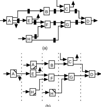
The circuit shown in Fig. 5 is an internally balanced structure but is not a balanced structure. The relation among three structures is shown in Fig. 6.
A
B C D
R1
R2 R3
Figure 5. Example of internally balanced structure
Sequential circuits of internally balanced structure
Sequential circuits of balanced structure Sequential circuits of
acyclic structure
Figure 6. Classification of sequential circuits by structure Theorem 1 [5]: The necessary and sufficient condition for realization of an FSM M as an acyclic structure is mk(I ) = O for any constant k, such that for k
> 1 we have mk(I) = m(mk-1(I )) and m1(I ) = m(I ). Lemma 1: The statement that an FSM M is expressed as mk(I ) = O for any k is equivalent to the statement that M can be realized by a finite input memory machine of length k (see Fig. 7). In addition, it is equivalent to the statement that any input sequence of length k becomes a synchronizing sequence [1] of M. Therefore, we can obtain the following corollary. Corollary 1: The necessary and sufficient condition for realization of an FSM M as an acyclic structure is that M can be realized by a finite input memory machine.
Proofs for Theorem 1 and Corollary 1 are given in [5]. A different proof can be done by using the following Lemma 2 and Corollary 2.
Lemma 2: Any sequential circuit of acyclic structure (Fig. 8) can be transformed into an equivalent circuit allowing realization with a finite input memory, by operations of retiming (Fig. 9) and logic duplication (Fig. 10).
Corollary 2: Any FSM allowing realization as an acyclic structure can be realized as an internally balanced structure.
Proof: A circuit allowing realization by a finite input memory (Fig. 7) can be transformed into an equivalent circuit of the type shown in Fig. 11 by retiming. This statement and Corollary 1 (or Lemma 2) constitute a theorem.
Theorem 3: An FSM exists which can be realized as an acyclic structure, but which cannot be realized as a balanced structure.
P r o o f : If, for any input x, an output z varies depending on the values of x in different time frames, then for the circuit realizing z, a number of paths exist which are characterized by different sequential depths required to reach z from x. Therefore, it cannot be realized as a balanced structure. QED
For example, in Fig. 12, output is determined by input x in the current time frame and by input x at some previous time frame. Therefore, there are two paths of different depth leading from x to z.
Combinational Circuit
Figure 7. Finite input memory realization
C1 C2 C3 Ck
x
y y y
y
1 2 3
k-1 y z y1 2
Figure 8. General acyclic structure
logic FF FF logic
n m m n n m
Figure 9. Retiming
logic
n m logic
n m
logic m
Figure 10. Logic duplication
Combinational Circuit
x y1 2 k
z
y y
Figure 11. Internally balanced structure
FF
AND
x y
z Figure 12. Circuit example
From Theorems 2 and 3 we can conclude the following (see Fig. 13):
{FSMs which can be realized as a sequential circuit of acyclic structure}
= {FSM which can be realized as a finite input memory machine}
= {FSMs which can be realized as a sequential circuit of internally balanced structure}
⊃ {FSMs which can be realized as a sequential circuit of balanced structure}.
FSMs realizable as acyclic structue FSMs realizable as finite input memory machine FSMs realizable as internally balanced structure
FSMs realizable as balanced structure
Figure 13. Classification of finite state machines
A
B E
H
F G
C
D
(a)
(b) A
B E
H
F G
C
D
H A
Figure 14. (a) Acyclic structure; (b) time expansion 3. Test Generation Complexity
3.1 Acyclic Structure
Fig. 14(a) illustrates an example of a sequential circuit with acyclic structure. For this circuit, the test pattern can be obtained by applying the test generation algorithm for combinational circuits to the time-expanded combinational circuit illustrated in Fig. 14 (b). Since there are several sub-circuit duplicates, we must consider the same fault in each sub-circuit, i.e., a kind of multiple faults. Assuming a sequential depth d, the time- expanded circuit will include in the worst case d+1 sub- circuit duplicates. After obtaining the test pattern for the
time-expanded combinational circuit, we can generate a test sequence (for the sequential circuit) corresponding to the test pattern. The length of the test sequence is d+1 in worst case.
3.2 Balanced Structure
Theorem 4 [3]: If a sequential circuit S is a balanced structure, S allows test generation with combinational test generation complexity.
The sequential circuit S shown in Fig. 4 is a balanced structure. Replacing all flip-flops in S by wires, a combinational circuit C(S) as shown in Fig. 15 is obtained. The test pattern is obtained by applying to this combinational circuit a combinational test generation algorithm (ATG). From the test pattern generated by the combinational ATG, we obtain the corresponding test sequence, taking time into account. Assuming a sequential depth d, the length of the test sequence is d+1 in worst case. In this test sequence, the same input values are applied to each primary input during d+1 clocks. An advantage of the sequential circuit with balanced structure is that it has time expansion to d+1, similarly for the acyclic structure, but there are no duplicates in the time-expanded circuit.
C1
C2
C3
C4
time frame 1 time frame 2 time frame 3 Figure 15. C-transformed combinational circuit C(S) 3.3 Internally Balanced Structure
Theorem 5: If a sequential circuit S is an internally balanced structure, S allows test generation with combinational test generation complexity.
Proof: First, we shall prove that if a fault f in S can be tested, then the fault fc in C*(S) corresponding to f can be tested in C*(S). It is sufficient to prove that a test pattern Tc for fc in C*(S) can be generated from the test sequence T for f in S. Here, we shall treat a fault at a primary input with fanout as a multiple fault which exits simultaneously in all the fanout branches of the input.
If the sequential depth of S is d, the length of T is d+1. Assume that f can be detected in a time frame t at primary output zk (1<t<d+1). From this test sequence T we can define the primary input value xi in C*(S) for the test pattern Tc as shown below.
(1) Case of xi not being a primary input resulting from separation:
The sequential depth from xi to zk is uniquely determined. Let the depth be dik. The value of xi
required to detect f in T at zk is the value of the primary input xi in time frame t–dik. Therefore, the primary input value xi in time frame t–dik in T can be set to define the primary input value xi of the test pattern Tc.
(2) Case of xi being a primary input resulting from separation:
Suppose that the original primary input value of xi in S is denoted x. Although x is a primary input in S, xi is not a primary input. In C*(S), xi is a primary input. Since this is the case of an internally balanced structure, we can uniquely determine the sequential depth from xi to zk, which is denoted as dik. The value of xi required to detect f in T at zk equals the x value in time frame t–dik. The x value in time frame t–dik in T is set to define the primary input value xi in the test pattern Tc.
It is evident that the test pattern Tc defined as described above will detect the fault fc in C*(S). Next, we prove that if the fault fc in C*(S) can be tested, then the fault f in S corresponding to fc can be tested in S. It is sufficient to prove that the test sequence T for f in S can be generated from the test pattern Tc in C*(S). Suppose fc can be detected at the primary output zk in the test pattern Tc. The primary input value xi of the test sequence T such that the fault f corresponding to fc can be detected at the primary output zk in time frame t is determined as follows.
(1) Case of xi not being a primary input resulting from separation:
The sequential depth from xi to zk is uniquely determined. Let the depth be dik. The primary input value in the test pattern Tc is set to the primary input value xi at the time frame t–dik of the test sequence T. (2) Case of xi being a primary input resulting from separation:
Assume that the primary input xi in S was separated to obtain the primary inputs xi1, xi2, ..., xin in C*(S). Since this is the case of an internally balanced structure, we can uniquely determine each sequential depth from xij to zk, which is denoted by dijk. Since these are separable, all d ijk (j=1,2,...,n) are different sequential depths. Therefore, all time frames (t–dijk) (j=1,2,...,n) are different, and can be set to n time frames in the test sequence T as described below. That is, the primary input values xij (j=1,2,..., n) of test pattern Tc are set to define the primary input value xi in time frames (t–dijk) (j=1,2,...,n) in the test sequence T.
It is evident that the test sequence T defined above can detect the fault f in S. QED
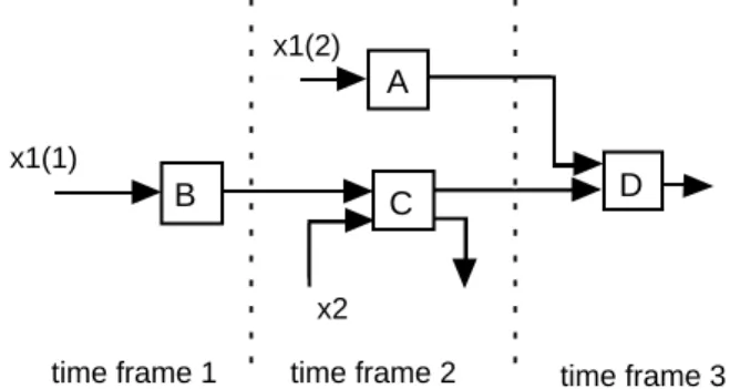
In Fig. 5, consider the C*-transformation of the sequential circuit S with internally balanced structure.
Since in S the input fanout branches which are fan outed at primary input x1 are separable, we separate them. Then, on replacing the flip-flops by wires, we obtain the combinational circuit C*(S) as shown in Fig. 16.
We can then obtain the test pattern for each fault in this C*-transformed combinational circuit by using a combinational ATG. Taking the time frame into account, we can construct the test sequence for the original sequential circuit. Assuming that the sequential depth of the circuit is d, the length of the test sequence is d+1 at most.
An advantage of sequential circuits with internally balanced structure is that there are no duplicates in the circuit which was time expanded to d+1, similarly for the case of balanced structures.
A
B C D
x1(1)
x1(2)
x2
time frame 1 time frame 2 time frame 3 Figure 16. C*-transformed circuit C*(S). We have introduced a new class of sequential circuits (internally balanced structures) with combinational test generation complexity (Theorem 5) which is larger than the class of sequential circuits of balanced structure. On the other hand, sequential circuits of acyclic structure do not necessarily allow test generation with combinational test generation complexity as illustrated in Fig. 3. From Theorem 3, it is not always possible for a FSM realizable as acyclic structure to be realized as balanced structure. However, from Corollary 2, any FSM realizable as acyclic structure can be also realized as internally balanced structure. Therefore, any sequential circuit of acyclic structure can be transformed or modified into an function-equivalent sequential circuit of internally balanced structure which is capable of test generation with combinational test generation complexity. In this sense, the class of sequential circuits of internally balanced structure might be one of the largest classes of sequential circuits with combinational test generation complexity.
4. New Definition of Possibility of Test Generation with Combinational Test Generation Complexity
In [3] the possibility of test generation with combinational test generation complexity was defined as follows: If the test generation problem for S can be reduced to the test generation problem of C-transformed combinational equivalent C(S), the sequential circuit S is said to be in a class of sequential circuits with combinational test generation complexity. In Section 2
we extended the definition of possibility of test generation with combinational test generation complexity by introducing an extended combinational transformation (C*-transformation).
Here we further extend the concept and introduce a new definition of the possibility of test generation with combinational test generation complexity by extending those transformations.
Pc: Combinational Test Generation Problem Instance: A combinational circuit C and a fault f. Question: Is there a test pattern to detect f in C? Ps: Sequential Test Generation Problem Instance: A sequential circuit S and a fault f. Question: Is there a test sequence to detect f in S? Pα: Class α Test Generation Problem
Instance: A sequential circuit S in α and a fault f. Question: Is there a test sequence to detect f in S? Let Tc(n) and Tα(n) be the time complexity of test generation problems Pc and Pα, respectively, where n is the size of a problem instance.
Reducibility: Problem A is reducible to problem B if there exits a transformation τ such that for any instance a ∈ A the solution of a is the same as the solution of τ(a)
∈ B.
Combinational Test Generation Complexity:
A class of sequential circuits, α, is called to have combinational test generation complexity if there exists a transformation τ such that
(1) Pα is reducible to Pc by transformation τ, and (2) for each S∈α, Tτ(size of S) ≤ Tc(size of S) and Tc(size of τ(S)) ≤ Tc(size of S),
where Tτ is the time complexity of transformation τ. From this definition, Tτ(size of S) +Tc(size of τ(S)) ≤ Tc(size of S). Therefore, the test generation problem of a sequential circuit S with combinational test generation complexity can be solved by first transforming S to τ(S) and then applying a combinational ATG to the transformed combinational circuit τ(S). The total time complexity is less than Tc(size of S), i.e., the time complexity of combinational test generation problem. As for the complexity of transformation Tτ, it must be less than the combinational test generation complexity Tc. However, by reason of the NP-completeness of the combinational test generation problem Pc, if one considers Tc might be O(2n) in worst case, where n is the number of gates in the circuit, then almost all circuits are in the class of sequential circuits with combinational test generation complexity, and our discussion becomes meaningless. Fortunately, it is known that Tc seems to be O(nk) for some constant k (less than 2) empirically. Therefore, when we devise a new transformation method to further expand the class of sequential circuits with combinational test generation complexity, we could consider Tτ to be less than O(nk) for practical use.
5. Conclusion
We have defined classes for sequential circuits allowing test generation with combinational test generation complexity, and have identified their characteristics. The acyclic structures do not exhibit these characteristics. We introduced a new class of internally balanced structures as a class that exhibits these characteristics. The FSMs that can be realized with acyclic structures can be also realized with internally balanced structures. Further, we introduced a new definition of test generation possibility with combinational test generation complexity.
References
[1] H. Fujiwara, Logic Testing and Design for Testability, The MIT Press, 1985.
[2] M. Abramovici, M. A. Breuer and A. D. Friedman, Digital Systems Testing and Testable Design, Computer Science Press, 1990.
[3] R. Gupta, R. Gupta and M. A. Breuer, "The BALLAST methodology for structured partial scan design," IEEE Trans. on Computers, Vol. C-39, No. 4, pp. 538-544, April 1990.
[4] A. Balakrishman and S.T. Chakradhar, "Sequential circuits with combinational test generation complexity," Proc. IEEE Int. Conf. VLSI Design, pp. 111-117, January 1996.
[5] A. D. Friedman and P.R. Menon, Theory and Design of Switching Circuits, Computer Science Press, 1975.
[6] C. E. Leiserson and J. B. Saxe, "Retiming synchronous circuitry," Algorithmica, Vol. 6, pp. 5- 35, 1991.
[7] A. Balakrishnan and S. T. Chakradhar, "Software transformations for sequential test generation," IEEE Asian Test Symp., pp. 266-272, Nov. 1995.
[8] R. Gupta and M. A. Breuer, "Testability properties of acyclic structures and applications to partial scan design," Proc. IEEE VLSI Test Symp., pp. 49-54, 1992.
[9] D. KIagaris and S. Tragoudas, "Partial scan with retiming," Proc. Design Automation Conf., pp. 249- 254, 1993.
[10] S. Dey and S. T. Chakradhar, "Design of testable sequential circuits by repositioning flip-flops," Journal of Electronic Testing: Theory and Applications, 7, pp.105-114, 1995.
[11] A. El-Maleh, T.E. Marchok, J. Rajski and W.Maly,
"Behavior and testability preservation under the retiming transform," IEEE Trans. on CAD, Vol. 16, No. 5, pp. 528-543, May 1997.
[12] H. Fujiwara, S. Ohtake and T. Takasaki, "Sequential circuit structure with combinational test generation complexity and its application," Trans. IEICE (DI), Vol. J80-D-I, No.2, pp. 155-163, 1997. (in Japanese) [13] T. Takasaki, T. Inoue and H. Fujiwara, "Partial scan
design methods based on internally balanced structure," Proc. Asia and South Pacific Design Automation Conference, pp. 211-216, Feb. 1998.
![Figure 6. Classification of sequential circuits by structure Theorem 1 [5]: The necessary and sufficient condition for realization of an FSM M as an acyclic structure is mk(I ) = O for any constant k, such that for k > 1 we have mk(I) = m(mk-](https://thumb-ap.123doks.com/thumbv2/123deta/5753834.27209/3.892.463.794.340.1133/classification-sequential-structure-necessary-sufficient-condition-realization-structure.webp)