F-Scan: An Approach to Functional RTL Scan for
Assignment Decision Diagrams
Marie Engelene J. Obien* and Hideo Fujiwara Abstract — This paper presents a new methodology for
functional Register Transfer Level (RTL) scan, in which existing functional elements and paths can be maximally utilized. The approach is called F-scan, which primarily aims to reduce the total area overhead due to augmentation for testing. Since the method allows for parallel scanning of test vectors, test application time is also made to be at the minimum. The case study shows the effectiveness of our approach compared to full scan design1.
Index Terms — Scan design, design-for-testability, functional RTL, assignment decision diagram.
I. INTRODUCTION
Testability of sequential circuits has been improved through a design for testability (DFT) technique called scan path insertion, since it reduces the sequential circuit test generation problem into a combinational one. Of the scan insertion methods to date, conventional full scan design (or full scan) is the most prevalent because it provides complete controllability and observability of any digital circuit, thus making testing tremendously easier. In full scan, each flip-flop is converted into a scan flip-flop and connected into a scan chain that allows straightforward scan-in and -out of test patterns. However, this is performed at the gate-level, which entails: 1) high area overhead brought about by DFT elements added per flip-flop and 2) long test application time due to the serial shifting of test vectors through the scan chain.
An astute approach to this problem is to deal with the circuit at a higher level of abstraction, hence reducing the amount of circuitry to be augmented for testability. Several works on scan insertion at structural [2-7] and functional [8,9] register- transfer level (RTL) circuits have been proposed. Gupta et al. [2] introduced a structured partial scan design that reduces area overhead by converting only the selected flip-flops into scan flip-flops. However, full scan approaches assure stronger testability of circuits as demonstrated by the rest of the reviewed works. H-Scan [3] utilizes paths between registers, but only through multiplexers. Orthogonal scan [4] uses datapath flow as scan path, of which the concept is similar with our proposed F-Scan. However, it also requires multiple test configurations if two or more paths share the same functional unit because it uses hold functions (load enable). A hold function is a logic that makes a register hold the same value when the function is activated. This is necessary when a
1 This work was supported in part by Japan Society for the Promotion of Science (JSPS) under Grants-in-Aid for Scientific Research (B) (No. 20300018).
M. E. J. Obien and H. Fujiwara are both with the Computer Design and Test Laboratory of the Graduate School of Information Science in Nara Institute of Science and Technology, Kansai Science City, 630-0192 Japan (email: [obien-j, fujiwara]@is.naist.jp).
functional logic is shared because it allows scanning-in and - out of vectors from scan paths one at a time. Our method does not employ this function because of the disadvantages of adding extra pins for controlling multiple paths during test and the expected longer test application time because simultaneous scan-in and -out cannot take place.
The following techniques provide complete fault efficiency aside from reducing area overhead. Wada et al. [5] introduced strong testability for data paths only. In [6], Ohtake et al. completed the method by dealing with both controller and datapath, but since they are separated, different approaches are used. Further improvements are given in [7], wherein there is no need for isolation between controller and datapath, thus the number of multiplexers added for test is reduced. However, this method requires a test controller to be added to the circuit. Our method is applied to circuits in assignment decision diagram (ADD), which represents the controller and datapath similarly so there is no need for separation. While other methods are applied on the controller or datapath only, our approach is uniform for the entire circuit.
The most related solutions to our work are Dependency scan (or D-scan) [8] and Huang’s RTL scan [9]. D-scan uses thru functions with predetermined control signals to organize scan paths in the circuit. This work, however, utilizes hold functions, which are not used by our method. Huang et al. [9], on the other hand, provided an effective approach for RTL scan by arranging registers in scan chains through cost rules to ensure the lowest possible area overhead for the circuit. Though this method tries to exploit available functional logic without the use of hold functions, mask function is not considered. A mask function can be applied to operation logic, wherein the value from one input can be passed through the output by masking the other inputs. This function further reduces area overhead and is used by our method.
Our novel approach to functional RTL scan is called F-scan, which improves all of the said works by introducing the concepts of functional scan-in and scan-out. The procedure efficiently organizes F-paths for scan by maximizing use of available functional logic, thus reducing area overhead due to test. It creates multiple scan paths that allow parallel and simultaneous scan-in and -out of test vectors in the circuit under test, which minimizes test application time. The proposed method is applied on functional RTL circuits in ADD because this allows faster test generation due to the determination of the test environment [11].
This paper is organized as follows. In Section II, we introduce ADD and define functional scan. In Section III, we explain our DFT method called F-Scan design. We describe the test environment generation in Section IV and present a case study in Section V. Conclusion is given in Section VI.
_____________________________ 589 978-1-4244-3870-9/09/$25.00 ©2009 IEEE
IEEE 8th International Conference on ASIC (ASICON2009), pp. 589- 592, Oct. 2009.
II. PRELIMINARY
This section provides a brief introduction about assignment decision diagrams and defines functional scan.
A. Assignment Decision Diagram
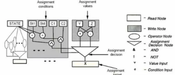
Assignment Decision Diagram or ADD is a representation developed for high-level synthesis that is complete, efficient, and partially unique. It consists of four parts as shown in Fig. 1: 1) the assignment value; 2) the assignment condition; 3) the assignment decision; and 4) the assignment target. There are four types of nodes needed to represent an ADD: read nodes and write nodes (primary inputs and outputs, registers), operation nodes, and assignment decision nodes or ADN (multiplexers) [10].
Fig. 1. The Assignment Decision Diagram and its four types of nodes.
B. Functional Scan
In order to discuss functional scan, we first introduce the nine symbol algebra used by Ghosh [11] for automatic test pattern generation (ATPG) of ADD circuits. Cg (general controllability) of a register means that it can be controlled to any arbitrary value. Cq (controllability to a constant) of a register is the ability to control the variable to any fixed constant value. It is clear that this symbol subsumes C0 (controllability to zero), C1 (controllability to one), and Ca1 (controllability to all one). O (observability) of an RTL variable is the ability to observe fault at a variable. Cs (controllability to a state) is similar to Cg but is applied to state registers to control to a particular state. Other symbols are Cz (controllability to the Z value) and O’ (complement observability), but these are not used for our study.
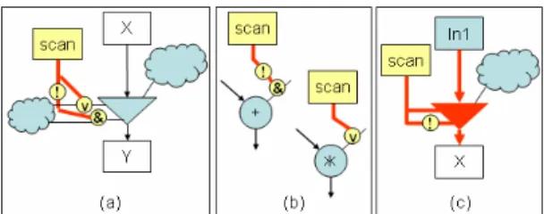
We use these symbols to show in Fig. 2 how functional scan takes place. In Fig. 2(a), we see that any value can be passed through an operation node as long as the other inputs to the node (side inputs) are constants. For addition and subtraction, the side input is Cq. For multiplication and division though, only C1 and Ca1 are allowed. For modulo, masking cannot be done so it is not utilized in any functional scan path. Any arbitrary value can also pass through an available ADN by manipulating its control inputs to C0 and C1. Similarly, we can observe through operation nodes and ADNs as shown in Fig. 2(b). Given these, we have the following definitions.
Definition 1. In order to functionally scan-in test vectors to an ADD circuit, available functional elements are utilized to assign any arbitrary values to all registers in the circuit from primary inputs while using constant values as side inputs. Fsi(n) is satisfied if any value can be functionally scanned-in
to register node n (output of operation node or ADN) from a primary input (with some clock cycles).
Definition 2. In order to functionally scan-out test vectors from an ADD circuit, available functional logic is utilized to retrieve values from all registers in the circuit through primary outputs while using constant values as side inputs. Fso(n) is satisfied if any value can be functionally scanned-out from register node n (input to an operation node or ADN) to a primary output (with some clock cycles).
Fig. 2. a) General controllability and b) observability of operation and assignment decision diagram nodes.
Fig. 3. Functional a) scan-in and b) scan-out as illustrated per node.
Fig. 3 illustrates how available functional logic can be exploited for testing. Each node can be Fsi(n) and Fso(n) by making side inputs Cq/C0/C1/Ca1, as determined according to the type of functional logic. This means that for operation nodes, since we know the constant value of the other input, we can compute for the value of the Fsi input such that any arbitrary number can be passed to the output to make it Fsi. In the same way, the value of an Fso input to an operation node can be computed in the Fso output using the constant value of the other input. For ADNs, any value can be passed or retrieved through the ADN by controlling which Fsi/Fso input of the ADN will pass its value to the Fsi/Fso output.
Definition 3. In functional scan (abbrev. F-scan), all registers are made Fsi and Fso to be used for functional scan function. F-scan is a concept that uses functional elements and paths to create scan chains for testing.
The difference between full scan and F-scan is that full scan arranges memory elements in single or multiple chains for shifting of test vectors while F-scan includes all registers in one or more scan chains called F-paths. While full scan augments multiplexers to connect flip-flops, F-scan exploits available functional elements and paths, hence resulting to lesser area overhead. Each F-path starts with a primary input and ends with a primary output. Test vectors are allowed to be functionally scanned-in and -out of the registers along the F- path given that the side inputs to the functional units are constants. F-paths also allow scan-in and -out test vectors simultaneously, thus, similar to full scan, only one test pin is needed to activate scan.
590
Definition 4. An ADD circuit is said to be F-scannable if each of the registers in the circuit is included in an F-path, wherein it is usable for F-scan.
III. DESIGN-FOR-TESTABILITY METHOD
We introduce a new functional RTL scan approach called F- Scan design, which makes any ADD circuit F-scannable. To do so, we organize F-paths using all of the registers in the ADD circuit. The algorithm is as follows.
Step 1. Identify the primary inputs and the registers containing constants in the circuit. The set of primary inputs is denoted as PI. The constants serve as F-scan side inputs.
Step 2. Build the weighted connectivity matrix of the ADD circuit with the following cost conditions:
1. If there is a direct link between registers, the cost is 0. 2. If there is a conditional transfer path denoted by ADN
between registers, the cost is equal to 1g + 2(# of control signals to ADN-1)g, where g is the unit for gates.
3. If there is an operational block (for modulo, do 4 instead) between two registers, we use the cost to add mask functions plus the cost to control the ADN. This cost is equal to 1(# of * or /)(bitwidth of line)g + 2(# of + or - )(bitwidth of line)g + 1g + 2(# of control signals to ADN- 1)g.
4. If there is entirely no connection between two registers, an additional interconnect and ADN will be needed to connect them. Thus, the cost is 3(bitwidth of line)g + 1g.
Step 3. According to the weighted connectivity matrix, organize the registers in such a way that the F-paths will need the least cost for additional hardware. The first time frame of each path will contain all the registers Fsi from the primary inputs. The next time frame will contain all registers Fsi by primary inputs and registers that are Fsi in the previous time frame. The procedure continues until all registers are Fsi. No two paths begin with the same primary input.
Step 4. Complete the F-paths by determining primary outputs (PO) that will terminate each path. Using the weighted connectivity matrix, we determine the connection to PO of each F-path with the least cost. No two paths can terminate at the same PO. This assures that parallel scan-in and scan-out can occur simultaneously.
After defining the F-paths, we modify the ADD circuit by adding DFT elements according to the costs per edge of the F- path graph. These are shown in Fig. 4. For state registers, we automatically add primary input and primary output (if no extra pins are available) and connect them directly to the state register through ADNs. This way, the state value can be controlled and observed directly, independent of the other parts of the circuit (i.e. datapath). Moreover, to further reduce test application time, trimming of the F-paths to have equal number of registers, whenever possible, can be done.
An example of the application of F-scan is given in Fig. 5. All registers and pins are 8-bit wide.
Fig. 4. DFT elements. a) ADN control augmentation for test, which corresponds to Cost Condition 2. b) Mask function augmentation corresponding to Cost Condition 3 if the lines are 1-bit. c) Additional ADN and interconnect corresponding to Cost Condition 4.
Fig. 5. Example 1. a) Original ADD circuit. b) F-Scanned version of the circuit. The DFT elements named test correspond to Fig. 5(a) while the DFT element for mask is shown in Fig. 5(b). c) The weighted connectivity matrix of the ADD circuit. d) The F-paths generated.
Fig. 6. F-scan environment for Example 1.
IV. TEST ENVIRONMENT GENERATION
The advantage of using ADD is that test environment can be used to make test pattern generation faster. We illustrate the F-scan test environment through Example 1 in Fig. 6.
The F-scan-in environment denotes the F-scan-in phase where all registers are scanned-in with test vectors, hence the last cycle in this phase is when all registers are Fsi. The test phase happens by setting the circuit to normal mode such that the all Fsi registers are used as input-registers and the same registers (also Fso) are used as output-registers for testing the circuit. The F-scan-out phase is shown by the F-scan-out environment where values in all Fso registers are scanned-out. During F-scan-out phase for Example 1, as the values from X and Y registers are shifted to the primary outputs, the primary inputs can simultaneously scan-in values to those registers. F- scan-in phase and F-scan-out-phase are overlapped, i.e. pipelined, after the first scan-in. For Example 1, F-scan-in and F-scan-out are both one cycle, and after the first scan-in, F- scan-in and F-scan-out can be done simultaneously in just one cycle until the last test vector. State registers are dealt with similarly in the same test environment, as it is included in a single F-path.
591
V. CASE STUDY
In order to present the effectiveness of our proposed method, we provide a motivational example of the application of F- Scan design to an ADD circuit, of which its results are compared with full scan and orthogonal scan. The original ADD circuit is given in Fig. 7(a). The augmented circuit through F-Scan, full scan, and orthogonal scan are shown in Fig. 7(b), (c), and (d), respectively. Each register and pin in the circuit is 32-bit wide. For simplicity, the state register and the control signals to ADNs are not shown. In complete circuits with state registers, additional PI and PO (if not yet available) are needed to control and observe the state values.
For this case study, we considered the type of full scan, which allows parallel scan-in and -out of test vectors using multiple paths. In orthogonal scan, we augmented the circuit by utilizing data paths for scan and opting to use hold functions to handle operation x, labeled in Fig. 7(a).
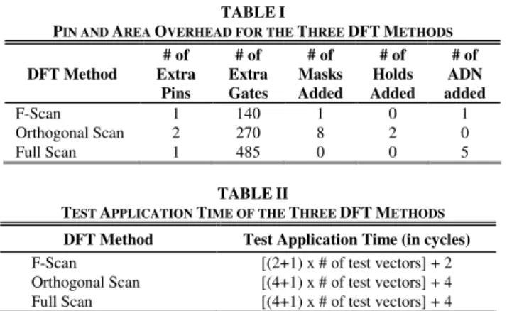
We evaluate pin and area overhead using Table I. Orthogonal scan has an extra pin overhead compared to F- Scan and full scan because of the hold function augmented to deal with operation x. The number of augmented gates for each method is computed according to the number of mask functions, hold functions, and ADNs added to the circuit. Moreover, as can be observed in Table II, F-Scan also has the shortest test application time because it only takes two cycles for simultaneous scan-in and scan-out of test vectors in the circuit. Since the DFT methods used are full scan approaches, the combinational area remains the same and hence, the lengths of test vectors are approximately equal.
TABLEI
PIN AND AREA OVERHEAD FOR THE THREE DFTMETHODS
DFT Method
# of Extra
Pins
# of Extra Gates
# of Masks Added
# of Holds Added
# of ADN added
F-Scan 1 140 1 0 1
Orthogonal Scan 2 270 8 2 0
Full Scan 1 485 0 0 5
TABLEII
TEST APPLICATION TIME OF THE THREE DFTMETHODS DFT Method Test Application Time (in cycles) F-Scan [(2+1) x # of test vectors] + 2 Orthogonal Scan [(4+1) x # of test vectors] + 4 Full Scan [(4+1) x # of test vectors] + 4
VI. CONCLUSION AND RECOMMENDATION
A novel approach to functional RTL scan called F-Scan has been proposed. It maximally utilizes available functional elements and paths in the circuit to insert scan paths for testing. It minimizes both area overhead compared to full scan design, as shown by the case study presented. Test application time is also kept at the minimum. Since ADD representation is used, faster test generation time is also expected.
Fig. 7. ADD Circuit A (a) and three DFT methods applied (b-d).
REFERENCES
[1] H. Fujiwara, Logic Testing and Design for Testability. Cambridge, MA: MIT Press, 1985.
[2] R. Gupta and M. A. Breuer, “Partial scan design of register transfer level circuits,” JETTA, Vol. 7, pp. 25-46, 1995.
[3] T. Asaka, S. Bhattacharya, S. Dey and M. Yoshida,“H-Scan+: A Practical Low-Overhead RTL Design-for-Testability Technique for Industrial Designs,” Proc. International Test Conference, pp. 265-274, 1997. [4] R. B. Norwood and E. J. McCluskey, “Orthogonal scan: Low
overhead scan for data paths,” Proc. Int. Test Conf., pp. 659–668, 1996. [5] H.Wada, T. Masuzawa, K. K. Saluja, and H. Fujiwara, “Design for
strong testability of RTL data paths to provide complete fault efficiency,” Proc. 13th Int. Conf. VLSI Des., pp. 300–305, 2000.
[6] S. Ohtake, H. Wada, T. Masuzawa, and H. Fujiwara, “A non-scan DFT method at register-transfer level to achieve complete fault efficiency,” Proc. Asia South Pacific Des. Autom. Conf., pp. 599–604, 2000.
[7] H. Fujiwara, H. Iwata, T. Yoneda, and C. Y. Ooi, "A Non-Scan Design for-Testability for Register-Transfer Level Circuits to Guarantee Linear- Depth Time Expansion Models," IEEE Trans. on Computer-Aided Des. of Integrated Circuits and Systems, Vol. 27, No. 9, pp. 1535-1544, 2008. [8] Chia Yee Ooi and Hideo Fujiwara,"A new scan design technique based
on pre-synthesis thru functions," Proc. 15th IEEE Asian Test Symposium, pp. 163-168, 2006.
[9] Y. Huang, C.C.Tsai, N. Mukhejee, O. Samman, D. Devries, W.T.Cheng, and S.M.Reddy, "Synthesis of scan chains for netlist descriptions at RT- level," JETTA, Vol. 18, pp. 189-201, 2002.
[10]V. Chaiyakul, D. D. Gajski, and L. Ramachandran, “High-level transformations for minimizing syntatic variances,” Proc. Design Automation Conf., pp. 413-418, 1993.
[11]I. Ghosh and M. Fujita, “Automatic Test Pattern Generation for Functional Register-Transfer Level Circuits Using Assignment Decision Diagrams,” IEEE Trans. Computer-Aided Design on Integrated Circuits and Systems, Vol. 20, No. 3, pp. 402-415, 2001.
592
![For copies of the original instructions see [7]](data:image/gif;base64,R0lGODlhAQABAIAAAP///wAAACH5BAEAAAAALAAAAAABAAEAAAICRAEAOw==)