A Method of Test Generation for Weakly Testable Data Paths
Using Test Knowledge Extracted from RTL Description
Satoshi Ohtake Michiko Inoue Hideo Fujiwara Graduate School of Information Science, Nara Institute of Science and Technology
8916-5, Takayama, Ikoma, Nara 630-0101, Japan E-mail: ohtake, kounoe, fujiwara @is.aist-nara.ac.jp
Abstract Weak testability[1] is a testability measure for register-transfer level (RTL) data paths. If a data path satis- fies weak testability, for each hardware element of the data path, there exist paths from some primary inputs to the el- ement to justify some values on its output and paths from the hardware element to some primary outputs to propa- gate some values on its output. For a weakly testable data path, a sequential ATPG tool can generate a test sequence with high fault efficiency in short test generation time[1]. In this paper, we introduce a notion calledtest knowledge, use of which by commercial ATPG tools can further decrease the test generation time and increase the fault efficiency in weakly testable data paths. This test knowledge is informa- tion which is relevant to structure of weakly testable data paths, and also easy to find. Use of this test knowledge to facilitate the test generation and increase the testability of data path is established in experimental results.
1. Introduction
Testing of large VLSI circuits is a well-known hard prob- lem. It is necessary to reduce the cost of testing and to en- hance the quality of testing. The cost of testing is estimated by test generation time and test application time. The qual- ity of testing is estimated by fault efficiency1. For combi- national circuits, combinational automatic test pattern gen- eration (ATPG) tools can generally generate tests with high fault efficiency in reasonable time[2]. On the other hand, high fault efficiency can not be achieved in sequential cir- cuits due to enormous time taken by sequential ATPG tools. To ease the complexity of test generation, design-for- testability (DFT) techniques are followed. The most com- monly used DFT techniques for sequential circuits are scan-based approaches[2]. These techniques can make ATPG easier and can improve fault efficiency. How- ever, these techniques have main disadvantage that at-speed testing[3] is impossible. To avoid such the problems of scan techniques, scientists often proposed some non-scan approaches. Moreover, any technique followed at gate level
1Fault efficiency is the ratio of the number of faults detected or proved redundant to the total number of faults.
faces the problems arising out of huge number of elements and high complexities of the circuits at that level. Thus test generation and DFT techniques were recently proposed at register-transfer level (RTL). The main advantage of con- sideration of DFT at RTL is as follows: complexity of DFT at RTL is much smaller than that at logic level because the number of elements under consideration at RTL is much smaller than that at logic level. Furthermore, since testa- bility is considered at RTL and then logic synthesis is ap- plied, we do not need to take consideration into testability at logic level and we can avoid such an undesirable result that the area and performance optimized in logic synthesis are spoiled by applying DFT at logic level.
In this paper, we consider the testing problems for data paths at RTL. In RTL description, a VLSI circuit generally consists of a controller and a data path. The former is rep- resented by a state transition graph and the latter is repre- sented by interconnection of registers and operational mod- ules. A sequential circuit synthesized from an RTL data path preserves the circuit structure of the RTL data path. Some non-scan DFT techniques for RTL data paths which allow at-speed testing were proposed by Dey et al.[4] and Takabatake et al.[1]. The latter is our previous work. The paper defined a testability measure called weak testability for RTL data paths and presented a DFT technique which introduced thru operation for some operational modules to make a given data path weakly testable. In literature [1], experimental results showed that hardware overhead of the DFT is very low. If a data path satisfies weak testabil- ity, for each hardware element of the data path, there ex- ist paths from some primary inputs to the hardware ele- ment to justify some values on its output and paths from the hardware element to some primary outputs to propa- gate some values on its output. In literature [1], experimen- tal results using a common commercial sequential ATPG tool also showed that a sequential circuit synthesized from weakly testable data path offers low test generation time and high fault efficiency in comparison to that from general data path. However, since an ATPG tool does not know justifi- cation/propagation paths considered at RTL, it has to search justification/propagation paths at logic level.
In this paper, given a weakly testable data path, we dis- IEEE the 8th Asian Test Symposium (ATS'99), pp. 5-12, Nov. 1999.
cuss a method of test generation for the weakly testable data path. In case of a given data path does not satisfy weak testability, we can make it weakly testable by the DFT method in [1]. For a weakly testable data path, we pro- pose to provide some pre-information to commercial ATPG tools using which the tools can further decrease test gen- eration and application time with maintaining or achieving high fault efficiency in weakly testable data path. This pre- information is called test knowledge. It is basically an early information of behavior or structure of circuits in the de- sign process. Use of such kind of early information was also proposed in [5, 6]. In literature [6], Vishakantaiah et al. proposed a method of test generation using test knowl- edge extracted from RTL description written in VHDL. In our proposed method, we find test knowledge early from the structure of the data path and using the test knowledge, a test generation algorithm can easily find paths to activate a fault and propagate an error of the fault. Thus we expect the reduction in test generation time by ATPG tools. The presented method has the following advantages:
1. Test generation time can be reduced. 2. Test application time can be reduced. 3. Fault efficiency can be improved.
4. It is applicable to commercial sequential ATPG tools (need not modify your ATPG tools).
This paper is organized as follows: Section 2 gives the definition of weak testability and shows properties of weakly testable data paths. In Section 3, we define test knowledge and propose a method of test generation. Sec- tion 4 presents some heuristics to estimate the effectiveness of the test knowledge. Section 5 shows experimental results of our method.
2. Preliminaries
In RTL description, a VLSI circuit generally consists of a controller and a data path. In this paper, we consider only data paths. Inputs of a data path of a VLSI can be classified as follows: primary inputs which are primary inputs of the VLSI and control inputs which are from a controller of the VLSI. Similarly, outputs of the data path of the VLSI can be classified as follows: primary outputs which are primary outputs of the VLSI and status outputs which are to the con- troller of the VLSI. In this paper, we assume that values on control inputs of a data path of a VLSI can be controlled di- rectly from outside of the VLSI and values on status outputs of the data path can be observed directly from outside of the VLSI.
A data path consists of hardware elements and lines, where a hardware element is a primary input, a primary output, a control input, a status output, a register, a mul- tiplexor, or an operational module, and a line connects two hardware elements with some bit width. Inputs of hardware elements of a data path can be classified into data inputs and control inputs. Data inputs of a hardware element are con- nected directly/indirectly from primary inputs of the data path. Control inputs of a hardware element are connected
directly from control input of the data path. Examples of control inputs of hardware elements are load enable signals of registers, selection signals of multiplexers and selection signals of functions of operational modules. Similarly, out- puts of hardware elements of a data path can be classified into data outputs and status outputs. Data outputs of a hard- ware element are connected directly/indirectly to primary outputs of the data path. Status outputs of a hardware el- ement are connected directly to status outputs of the data path.
In this section, we introduce testability measure for data paths weak testability and discuss the properties of data paths which satisfy weak testability.
2.1. Weak Testability Definition 1 Thru operation [1]
Let M be an operational module andFM be a set of func- tions which M provides. An operational module M is thru moduleif the following holds.
fth FM i fth X1 Xi Xn Xi. The above operation is called thru operation on Xiand the input Xiis called a thru input.
If an input X is a thru input, X is denoted by ˆX. LetI NH denote a set of inputs of an hardware element H. Let H1and H2be hardware elements, and X be an input of a hardware element. Let H1 X(resp. H1 H2) means that there is a line connecting the output of H1and X (resp. some input of H2).
In the rest of this paper, we consider that a multiplexer is an operational module whose every input is thru input.
Here, we introduce weak controllability/observability of a hardware element. Intuitively, weak controllability (resp. observability) of a hardware element H means that some value (not necessarily any) on the output of H can be justi- fied (resp. propagated) from primary inputs (resp. outputs). Weak controllability is defined recursively from the primary inputs; a hardware element is weakly controllable, if all its inputs or at least one of its thru inputs are weakly control- lable.
Definition 2 Weak controllability [1]
A set of weakly controllable hardware elements is the min- imum setHwcsatisfying the following conditions.
1) For any primary input I, I Hwc.
2) For any register H, Hwc HwcHwc H H Hwc. 3) For any operational module M,
X I NM Hwc Hwc Hwc X Xˆ I NM Hwc Hwc Hwc Xˆ
M Hwc.
It can be considered that some value of some input of a hardware element is propagated (in a weak sense) to its output either if the input is thru input or if all other inputs are weakly controllable. Weak observability is defined re- cursively from the primary outputs; a hardware element is weakly observable, if its output values can be propagated (in a weak sense) to an output of some weakly observable hardware element.
X1 X2 X1 X2 X1 X2 X1 X2
PI1 PI2
m10 m9
mask1 mask2
MULT2 SUB1
MULT1 ADD1
0 1
m5 m40 1
1
0 m6 1 0m8
0 1
m1 m20 1
0 m11 1
LAT1
l1 REG1
LAT2
l2 REG2 l4 REG4
0 1
m3 REG5 l5
0 m71 REG3 l3
0 1 1 0 one
one one
PO1 PO2
MUX9
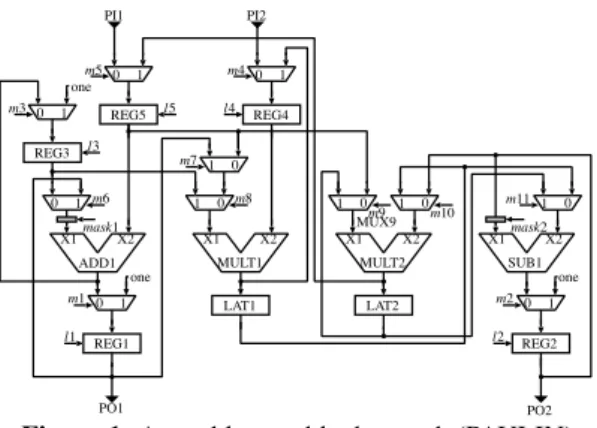
Figure 1: A weakly testable data path (PAULIN).
Definition 3 Weak observability [1]
A set of weakly observable hardware elements is the mini- mum setHwosatisfying the following conditions.
1) For any primary output O, O Hwo. 2) For any hardware element H,
Hwo Hwo
X I NHwo H X X I NHwo X
H X Hwc Hwc Hwc X
Xˆ I NHwo H Xˆ H Hwo.
Definition 4 Weak testability [1]
A data path DP is weakly testable iff all registers in DP are weakly controllable and weakly observable.
It is obvious from the definition that, if all registers in a data path are weakly controllable, all registers are also weakly observable, that is, the data path is weakly testable. Example 1 Weakly testable data path
An example of weakly testable data paths is as shown in Figure 1. It was transformed from the data path of Paulin in [7] by the DFT method of [1]. This includes mask ele- ments, where a mask element realizes a thru operation. In the figure, ADD, MULT, and SUB denote operational mod- ules adder, multiplier, and subtracter, respectively. REG and LAT denote register with load enable signal and with- out that, respectively. Hardware elements which have con- trol signals from m1 to m11 denote multiplexers. Similarly, hardware elements which have control signals mask1 and mask2 denote mask elements of ADD1 and SUB1, respec- tively.
2.2. Properties of Weakly Testable Data Paths Let H be a hardware element of a weakly testable data path. We define a set of paths in the weakly testable data path which makes H weakly controllable called a set of weakly controllable paths of H and that which makes H weakly observable called a set of weakly observable paths of H.
First, we define a set of weakly justification paths. We consider that weakly controllability of an input X of a hard- ware element and weakly controllability of the output of
X1 X2 X1 X2 X1 X2 X1 X2
PI1 PI2
m10 m9
mask1 mask2
MULT2 SUB1
MULT1 ADD1
0 1
m5 m40 1
1
0 m6 1 0m8
0 1
m1 m20 1
0 m11 1
LAT1
l1 REG1
LAT2
l2 REG2 l4 REG4
0 1
m3 REG5 l5
0 m71 REG3 l3
0 1 1 0 one
one one
PO1 PO2
Justification path
MUX8 MUX9 MUX7
MUX10 MUX5
Figure 2: A set of weakly controllable paths of MUX9.
a hardware element H which has connection H X are equivalent.
Definition 5 A set of weakly justification paths
Let X be an input of H. Let J be a set of some paths from primary inputs to X and letHJbe a set of hardware elements on J. Let DPJbe a data path which consists ofHJand J. Here, we allow DPJto have hardware elements which have inputs connected from no hardware element. We assume that these such inputs are not weakly controllable. If J is a minimal set of paths that makes X weakly controllable on DPJ, J is called a set of weakly justification paths of X . Definition 6 A set of weakly controllable paths
Let Xi i 1 2 n be an input of H where n is the number of inputs of H. Let Jibe a set of weakly justification path of Xi. Then
n
i 1
Jiis called a set of weakly controllable paths of H.
Definition 7 A set of weakly observable paths
A path from the output of H to primary outputs is called a propagation path of H. Let P be a propagation path of H. Let m be the number of operational modules on P such that whose input on P is not thru input, and let PHi i 1 2 m be such an operational module. Let nbe the number of inputs of PHi which are not on P and Xi j j 1 2 n be such an input of PHi. Let Ji jbe a set of weakly justification paths of Xi j. A set of paths P and
m
i 1 n
j 1
Ji jis called a set of weakly observable paths of H. Example 2 A set of weakly controllable path
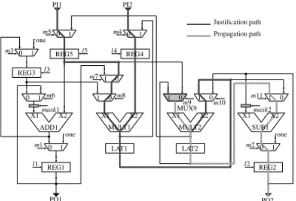
We consider the weakly testable data path shown in Fig- ure 1. A set of weakly controllable paths of a multiplexer MUX9 is shown in Figure 2.
Example 3 A set of weakly observable path
We consider MUX9 in Figure 1. A set of weakly observable paths of MUX9 is shown in Figure 3.
From Definition 4, for any hardware element H in a weakly testable data path, it is guaranteed that there exists a set of weakly controllable paths of H and a set of weakly ob- servable paths of H. Notice that, in weak testability, control
X1 X2 X1 X2 X1 X2 X1 X2
PI1 PI2
m10 m9
mask1 mask2
MULT2 SUB1
MULT1 ADD1
0 1
m5 m40 1
1
0 m6 1 0m8
0 1
m1 m20 1
0 m11 1
LAT1
l1 REG1
LAT2
l2 REG2 l4 REG4
0 1
m3 REG5 l5
0 m71 REG3 l3
0 1 1 0 one
one one
PO1 PO2
Justification path Propagation path
MUX9
Figure 3: A set of weakly observable paths of MUX9. timing of load enable signals of registers, selection signals of multiplexers and selection signals of functions of opera- tional modules and dependencies between values on inputs and that on output of a operational modules are not consid- ered. Therefore, it is not guaranteed that any value on any input of H is justified from primary inputs and any value on the output of H is propagated to some primary output (if it can be guaranteed, the data path is strongly testable[8]). However, for weakly testable data paths, experimental re- sults in [1] showed that high fault efficiency can be achieved with short test generation time and hardware overhead to make weakly testable is very low.
3. Test Knowledge to Assist ATPG 3.1. Overview of Our Approach
For a sequential circuit synthesized from a weakly test- able data path, most faults in the circuit can be activated from primary inputs and errors of these faults can be prop- agated to primary output using a set of weakly controllable paths and a set of weakly observable paths. However, in normal test generation for these faults, an ATPG tool has to search justification/propagation paths at logic level without using sets of weakly controllable paths and sets of weakly observable paths considered at RTL. If we can inform ATPG tools of existence of these paths called test knowledge, we can expect that test generation time and test application time can be decreased. In test generation of a fault of the se- quential circuit, to inform an ATPG tool of appropriate test knowledge, we consider to fix some values on control in- puts of the sequential circuit during generating a test of the fault.
3.2. Test Knowledge
Inputs of a data path are of two types, primary inputs and control inputs. These control inputs of the data path are connected to control inputs of hardware elements of the data path. If we fix some values on the control inputs, paths which propagate data from primary inputs to primary out- puts of the data path can be activated topologically. Ap- plying a value on control inputs of a data path to activate a
Table 1: Coordinate intersection.
0 1 χ ψ
0 0 ψ 0 ψ
1 ψ 1 1 ψ
χ 0 1 χ ψ
ψ ψ ψ ψ ψ
χ = don’t care, ψ = can’t specify
path from a hardware element to another hardware element is called forming the path defined as follows.
Definition 8 Path formation
For a hardware element H of a weakly testable data path, let C and O be a set of weakly controllable paths of H and a set of weakly observable paths of H, respectively. Let pi i 1 2 n be a path in C O where n is the number of paths in C O. Let Vi ci1 ci2 cim be a vector of values of control inputs of the data path where m is the number of control inputs of the data path. If ci jis a value of a selection signal for some thru input which exists on pi, ci jis the value (‘0’ or ‘1’) to enable the thru operation. Otherwise, ci jis a don’t care ‘χ’. The vector Viis called an activating vector of pi. Then applying the activating vector Vito the control inputs of the data path is called forming the path pi. Example 4 An activating vector
In Figure 2, we consider a path p as follows: PI1 MUX5
REG5 MUX7 MUX8 MULT1 LAT1
MUX10 LAT2 MUX9. The activating vector of p is m1, m2, m3, m4, m5, m6, m7, m8, m9, m10, m11, l1, l2, l3, l4, l5, mask1, mask2 χ, χ, χ, χ, 0, χ, 0, 0, χ, 1, χ, χ, χ, χ, χ, χ, χ, χ .
For each hardware element H in a weakly testable data path, there exist a set of weakly controllable paths C of H and a set of weakly observable paths O of H as mentioned above. However, some paths in C Omay not be formed simultaneously due to the conflict of control values. First, we define intersection of activating vectors as follows. Definition 9 Intersection of activating vectors
Let H be a hardware element of a weakly testable data path and let C and O be a set of weakly controllable paths of H and a set of weakly observable paths of H, respectively. Let pi and pj be two paths in C Oand let Viand Vjbe an activating vector of piand that of pj, respectively. The intersection Vi Vj formed from the respective coordinate intersections in Table 1 is said to be the intersection of acti- vating vectors Viand Vj.
Notice that, in Table 1, ψ denote that we can not specify a value on the coordinate.
Then conflict of control values are defined as follows. Definition 10 Conflict of control values
Let H be a hardware element of a weakly testable data path and let C and O be a set of weakly controllable paths of H and a set of weakly observable paths of H, respectively. Let piand pjbe two paths in C Oand let Vi ci1 ci2 cim
and Vj cj1 cj2 cjm be an activating vector of piand that of pj, respectively, where m is the number of control inputs of the data path. If a coordinate intersection cik
cjk k 1 2 m is ψ, we say that a conflict of control valuesoccurs on k-th coordinate of Viand Vj.
Therefore, in general, for a test generation of a fault of H, we can not fix some values on control inputs which is re- quired to form paths in C Oduring generating tests of the fault. We define a test knowledge of H giving consideration to this point as follows.
Definition 11 Test knowledge
For a hardware element H in a weakly testable data path, let Cbe a set of weakly controllable paths of H and let O be a set of weakly observable paths of H. Let pi i 1 2 n be a path in C Oand let Vi i 1 2 m be an activating vector of piwhere n and m be the number of paths in C O and that of control inputs of the data path, respectively. Let Kis a vector of values of control inputs of the data path such that
m
i 1
Vi. Such K is said to be a test knowledge of H with respect to C and O.
In general, a test knowledge of H with respect to C and O contains ‘0’, ‘1’, ‘χ’, and ‘ψ’. In our test generation method, for faults in H, we fix each value of a coordinate which is ‘0’ or ‘1’ of the test knowledge on control inputs of the weakly testable data path during generating tests of these faults.
Example 5 Test knowledge
We consider a hardware element MUX9 in Figure 1. We suppose that a set of weakly controllable paths and a set of weakly observable paths of MUX9 are selected as Figures 2 and 3, respectively. In this case, a test knowledge of MUX9 is as follows: m1, m2, m3, m4, m5, m6, m7, m8, m9, m10, m11, l1, l2, l3, l4, l5, mask1, mask2 χ, 0, χ, 0, 0, χ, 0, 0, ψ, 1, 1, χ, χ, χ, χ, χ, χ, 1 .
For each hardware element H of a weakly testable data path, since there exists one or more sets of weakly controllable paths of H and two or more sets of weakly observable paths of H, we can derive two or more test knowledges of H with respect to a pair of a set weakly controllable paths and a set of weakly observable paths. It is conceivable that selection of a test knowledge of H affects test generation time and test application time of faults in H and quality of tests of these faults. Therefore, we propose some heuristic measures to estimate test knowledge in Section 4 and show effectiveness of these heuristic measures by experiments in Section 5. 3.3. A Method of Test Generation
In our method, we assume that a weakly testable data path and its synthesized circuit are given. If only a data path which is not weakly testable is given, we can make it weakly testable by the DFT method of [1]. If only a data path described in behavioral level, we also make it weakly testable data path using the method of high-level synthesis for testability proposed in [9]. In the case of synthesized circuit is not given, we can derive it by synthesizing the given weakly testable data path using logic synthesis tool. We assume that there exists a one-to-one mapping between a hardware element of the given data path and subcircuit of its synthesized circuit and such mapping is known. The method consists of the following steps.
Step 1 Extract test knowledge
For each hardware element H of a weakly testable data path, first, we extract a set of weakly controllable paths C of H and a set of weakly observable paths O of H. Then we derive a test knowledge of H with respect to C and O. Step 2 Make fault lists
For each hardware element H of the weakly testable data path, we make a fault list which include a subset of faults of the subcircuit corresponding to H in a given synthesized circuit. Notice that, for some faults, since time required to generate tests of these faults or to identify that these faults are redundant may be long, we do not deal with some faults in this step. These faults are considered at the last step of this method. Details of this is discussed in Section 4. Step 3 Generate tests using test knowledge
For each hardware element H of the weakly testable data path, we generate tests of faults listed in the fault list corre- sponding to H for the given synthesized circuit using the test knowledge of H. We iterate the following steps till when trial of test generation for all faults is finished.
Step 3. 1 For faults listed in a fault list which is never tried to generate tests, we try to generate tests using test knowl- edge corresponding to the fault list. The test knowledge is informed to a sequential ATPG tool by fixing control val- ues of the test knowledge to some control inputs during test generation of these faults.
Step 3. 2 We perform fault simulation for faults in remain- ing fault lists which are not tried to generate tests using test sequences generated at the previous step. We except faults detected at this fault simulation from remaining fault list. Step 4 Generate tests without test knowledge
For each fault which could not be generated tests at previous step and faults which are not included at Step 2, we try to generate tests again without using test knowledge.
Notice that, in this method, we restrict search space of se- quential ATPG by informing test knowledge to sequential ATPG tools. It is generally conceivable that faults which could not be generated tests at the third step contain some testable faults. Therefore, we need to perform the forth step.
4. Estimating Effectiveness of Test Knowledge In general, for each hardware element H of a weakly testable data path, there exist two or more test knowledges of H as mentioned above. In this section, to select an effective test knowledge, we propose five heuristic mea- sures to estimate effectiveness of these test knowledges. We discuss these heuristic measures in order of effectiveness which is obtained from our preliminary experiments. In our preliminary experiments and proper experiments, we used a logic synthesis tool AutoLogicII (MentorGraphics) with sample libraries of MentorGraphics and a sequential ATPG tool TestGen (SunriseTestSystems)[10] on Ultra2 (SunMi- crosystems) workstation.
Heuristic Measure 1 Thru operation of operational mod- ule under test generation
Weak testability of data paths is defined for fault free data
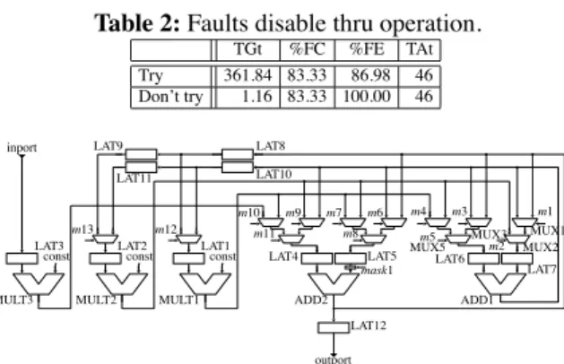
Table 2: Faults disable thru operation.
TGt %FC %FE TAt Try 361.84 83.33 86.98 46 Don’t try 1.16 83.33 100.00 46
outport
inport LAT8
MULT3 const
MULT2 const
MULT1 const
LAT12 m13
LAT1 LAT2 LAT3
m12 m10
m11 m9
ADD2
LAT4 LAT5
m8
m7 m6 m4
m5 m3
ADD1
LAT6 LAT7
m2 m1 LAT9
LAT10 LAT11
mask1
MUX1 MUX2 MUX3 MUX5
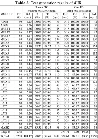
Figure 4: A weakly testable data path (4IIR).
paths. Suppose H is a hardware element in a weakly testable data path under test generation with a test knowledge with respect to a set of controllable paths C, where H has a thru input X and C includes a path to some other input X of H via the input X . We call such a path a loop. We consider that, in test generation of H under such test knowledge, we have to justify values on X by way of H itself and some fault f in H may cause to fail in such justification. In this case, it is conceivable that time required to generate test of f or to identify that f is redundant becomes long. There- fore, if there exists a test knowledge which makes no loop, we select the test knowledge. Otherwise, we do not try to generate tests for these faults at the third test generation step of our method and try them at the forth step.
Preliminary Experiment 1 An experimental basis of Heu- ristic Measure 1
Here, we consider generating tests for faults in a mask el- ement of ADD1 of the weakly testable data path shown in Figure 1. In this case, the thru operation is needed to jus- tify values on input X1 of ADD1. However, if there exists a fault f of the mask element which disables the thru op- eration, we can not justify values on the input X1. Table 2 shows test generation results of the third step of our method for the mask element of ADD1. In the table, rows “Try” and
“Don’t try” denote that all faults in the mask element were tried and all faults except for faults which disable the thru operation in the mask element, respectively. Notice that, in row “Don’t try”, we assume that faults which are not tried are untestable faults. Columns “TGt”, “%FC”, “%FE”, and
“TAt” denote test generation time in second, fault coverage, fault efficiency, and the length of a test generated, respec- tively. From this results, it is conceivable that time required to generate a test of f or to identify that f is redundant is long. Therefore, we had better to ignore faults which dis- able the thru operation at the third step.
Heuristic Measure 2 Reconvergent fanout
A pair of paths p1 and p2 which are from a hardware el- ement H1 to the other hardware element H2 such that all registers on these paths do not have load enable signals and p1and p2have the same number of registers is said to be a same depth reconvergent fanout. It is conceivable that a test knowledge makes some same depth reconvergent fanout,
Table 3: Reconvergent fanout.
TGt %FC %FE TAt Exists 0.28 98.96 100.00 30 Doesn’t exist 0.19 100.00 100.00 42
the number of values which can be justified from primary inputs on the output of the reconvergent element becomes small. Therefore, if there exists a test knowledge which does not make reconvergent fanout, we select such a test knowledge.
Preliminary Experiment 2 An experimental basis of Heu- ristic Measure 2
Here, we consider test generation for faults in ADD1 in weakly testable data path shown in Figure 4. The weakly testable data path was transformed from the 4th order IIR cascade filter in [1] by the DFT method of [1]. Table 3 shows test generation results of ADD1. Rows “Exists” and “Doesn’t exist” denote test generation result using test knowledge which forms a same depth reconvergent fanout
as follows: ADD2 MUX1 MUX2 LAT7 ADD1
and ADD2 MUX3 MUX5 LAT6 ADD1, and
that using test knowledge which does not form same depth reconvergent fanouts. The lower result is better than upper one. Therefore, if there exists a test knowledge which does not form same depth reconvergent fanouts, we had better to use it.
Heuristic Measure 3 Function of operational modules Since data are propagated by way of operational modules on paths formed by a test knowledge, some value may not be justified/propagated from/to primary inputs/outputs by their functions. Therefore, for a hardware element H, we select a set of weakly controllable paths of H which can justify the maximum number of values on the inputs of H and a set of weakly observable paths of H which can propagate the maximum number of values on the output of H. And then, we derive a test knowledge from them.
Heuristic Measure 4 Conflict of control values
Suppose H is a hardware element of a weakly testable data path and C and O are a set of weakly controllable paths of H and a set of weakly observable paths of H, respectively. If conflicts of control values occur on some control inputs of activating vectors Viand Vjof paths piand pjin C O, re- spectively, since such values can not be fixed on these con- trol inputs, we can not reduce search space of ATPG corre- sponding to these such control input. Therefore, to derive a test knowledge which has the largest number of specified values, we select an appropriate pair of a set of weakly con- trollable paths and a set of weakly observable paths. Heuristic Measure 5 Cost of testing
It is conceivable that test generation time for data paths depends on the number of clock cycles necessary to justi- fy/propagate values of registers from/to primary inputs/out- puts. Test application time (the length of tests) is also de- pends on such the number of clock cycles. In our approach, such the number of clock cycles is depend on test knowl- edge. Here, we introduce a measure to estimate time re- quired to generate/apply tests called weak testability cost as
Table 4: Weak testability cost.
Cost TGt %FC %FE TAt 9 0.22 100.00 100.00 64 8 0.19 100.00 100.00 42
Table 5: Characteristics of benchmark circuits.
circuit bit #add #sub #mult #mux #reg(#L/H) #th
4IIR 10 2 0 3 13 12(0) 1
Paulin 32 1 1 2 11 7(5) 2
follows.
Definition 12 Weak testability cost
Suppose H is a hardware element in a weakly testable data path and C and O are a set of weak controllable paths of H and a set of weak observable paths of H, respectively. Let n and m be the number of paths in C and O, respec- tively, and let pCi i 1 2 n and pO j j 1 2 m be paths in C and O, respectively. Let DpCi and DpO j be the number of registers on pCiand pO j, respectively. Let D be max DpCi max DpO j . Such D is said to be weak testability costof the test knowledge of H with respect to C and O.
We select a test knowledge which has the smallest weak testability cost.
Preliminary Experiment 3 An experimental basis of Heu- ristic Measure 5
Here, we consider test generation for faults in ADD1 in the weakly testable data path shown in Figure 4. Table 4 shows test generation results of ADD1 using two test knowledges which have different weak testability cost each other. From this results, smaller one is better in test generation time and test application time. Therefore, we had better to use test knowledge which has the smallest weak testability cost.
For a hardware element of a weakly testable data path, we select a test knowledge of the hardware element satisfy- ing these five measures possibly as the above order.
5. Experimental Results
We show experimental results with two benchmarks the 4th order IIR cascade filter[1] (4IIR for short) and the data path of Paulin[7] (PAULIN for short). We made these data paths weakly testable using the DFT method of [1]. Weakly testable 4IIR and weakly testable PAULIN are shown in Figures 4 and 1, respectively.
Circuit characteristics of these weakly testable data paths are shown in Table 5. Columns “ bit ”, “#add”, “#sub”,
“#mult”, “#mux” “#reg” and “#th” show bit width of data paths, the numbers of adders, subtracters, multipliers, mul- tiplexers, registers, and thru operations which are added by the DFT method, respectively. In column “#reg”, a number in parenthesis shows the number of registers which have load enable signals.
Tables 6 and 7 show test generation results of synthe- sized 4IIR and PAULIN, respectively. We experimented normal test generation (without test knowledge) and our method using test knowledge. In this experiment, to esti- mate heuristic measure, we extract test knowledge exactly
Table 6: Test generation results of 4IIR.
Normal TG Our TG
(without test knowledge) (using test knowledge)
MODULE Flt TGt FC FE TAt TGt FC FE TAt
(#) (sec.) (%) (%) (cyc.) (sec.) (%) (%) (cyc.) ADD1 96 0.23 100.00 100.00 36 0.19 100.00 100.00 42 ADD2 96 0.26 100.00 100.00 52 0.16 100.00 100.00 30 MULT1 86 0.36 100.00 100.00 68 0.18 100.00 100.00 36 MULT2 86 0.37 100.00 100.00 86 0.18 100.00 100.00 42 MULT3 86 12.27 100.00 100.00 32 0.09 100.00 100.00 12 MUX1 80 0.83 100.00 100.00 184 0.33 100.00 100.00 100 MUX2 80 0.44 100.00 100.00 96 0.24 100.00 100.00 72 MUX3 80 14.49 98.75 98.75 116 0.43 100.00 100.00 124 MUX4 80 28.26 100.00 100.00 166 0.29 100.00 100.00 76 MUX5 80 0.44 100.00 100.00 88 0.38 100.00 100.00 112 MUX6 80 0.28 100.00 100.00 48 0.32 100.00 100.00 94 MUX7 80 10.58 100.00 100.00 146 0.31 100.00 100.00 92 MUX8 80 0.44 100.00 100.00 100 0.22 100.00 100.00 60 MUX9 80 0.52 100.00 100.00 132 0.21 100.00 100.00 56 MUX10 80 135.45 87.50 87.50 184 0.21 87.50 100.00 60 MUX11 80 142.97 87.50 88.75 110 0.17 87.50 100.00 52 MUX12 80 0.59 100.00 100.00 132 0.34 100.00 100.00 108 MUX13 80 0.68 100.00 100.00 156 0.36 100.00 100.00 122 LAT1 60 0.24 66.67 100.00 48 0.20 66.67 100.00 36 LAT2 60 0.23 66.67 100.00 56 0.17 66.67 100.00 42 LAT3 60 2.18 66.67 100.00 20 0.11 66.67 100.00 12 LAT4 60 7.10 66.67 100.00 20 0.13 66.67 100.00 18 LAT5 60 0.16 66.67 100.00 24 0.18 66.67 100.00 32 LAT6 60 0.30 66.67 100.00 50 0.18 66.67 100.00 42 LAT7 60 0.26 66.67 100.00 50 0.19 66.67 100.00 28 LAT8 60 0.25 66.67 100.00 48 0.18 66.67 100.00 36 LAT9 60 0.26 66.67 100.00 56 0.20 66.67 100.00 42 LAT10 60 0.48 66.67 100.00 70 0.21 66.67 100.00 60 LAT11 60 0.28 66.67 100.00 52 0.24 66.67 100.00 60 LAT12 60 0.15 66.67 100.00 18 0.12 66.67 100.00 24 MASK1 60 123.07 83.33 83.33 38 0.18 83.33 100.00 38
(Step 4) (270) – – – – 371.71 0.00 89.26 0
TOTAL 2270 484.42 88.07 98.67 2482 378.61 88.11 98.72 1760
by hand. In our method, we informed TestGen of test knowledge as test generation constraint. To evaluate ef- fectiveness of test knowledge, we did not perform Step 3.2 described in Section 3.3. For both those tables, columns
“MODULE”, “#Flt”, “Normal TG”, and “Our TG” show name of hardware element of the data path, the number of faults in each modules, results of normal test generation, and that of our method, respectively. In columns “Nor- mal TG” and “Our TG” of both these tables, columns “TGt (sec.), “%FC”, “%FE”, and “TAt (cyc.)” show test genera- tion time in second, fault coverage (%), fault efficiency (%), and the number of clock cycles required for test application (the length of tests), respectively. In our results, we used five measures discussed in Section 4 to select test knowl- edge. Notice that, column “%FE” in “Our TG” shows fault efficiency in case that test knowledges were applied as test generation constraints. In this case, the ATPG tool might identify that some faults are redundant under fixing some values of the test knowledge on control inputs of the syn- thesized circuits. Therefore, we had to perform Step 4 de- scribed in Section 3.3. For both tables, the result of Step 4 is shown in row “(Step 4)”. Row “(Step 4)” of column
“#Flt” shows the number of faults which had to be retried to generate tests. Row “TOTAL” shows the total amount.
In the results of 4IIR, for MUX10, MUX11 and MASK1, use of test knowledge can drastically decrease test genera-
Table 7: Test generation results of PAULIN.
Normal TG Our TG
(without test knowledge) (using test knowledge)
MODULE Flt TGt FC FE TAt TGt FC FE TAt
(#) (sec.) (%) (%) (cyc.) (sec.) (%) (%) (cyc.) ADD1 316 1.49 100.00 100.00 62 1.10 100.00 100.00 44 MULT1 8260 102.27 100.00 100.00 164 18.30 100.00 100.00 120 MULT2 8260 48.70 99.98 99.98 248 19.84 100.00 100.00 142 SUB1 448 27.36 100.00 100.00 74 1.35 100.00 100.00 38 MUX1 196 0.91 100.00 100.00 38 0.96 100.00 100.00 30 MUX2 196 1.20 100.00 100.00 50 1.28 100.00 100.00 50 MUX3 196 1.63 100.00 100.00 64 1.91 100.00 100.00 76 MUX4 256 16.58 100.00 100.00 118 3.57 100.00 100.00 80 MUX5 256 16.95 100.00 100.00 88 4.64 100.00 100.00 68 MUX6 256 1.67 100.00 100.00 80 86.98 100.00 100.00 122 MUX7 256 58.79 100.00 100.00 121 13.45 100.00 100.00 64 MUX8 256 66.70 100.00 100.00 116 24.48 100.00 100.00 88 MUX9 256 10.99 100.00 100.00 144 2.81 100.00 100.00 56 MUX10 256 16.61 100.00 100.00 74 4.31 100.00 100.00 70 MUX11 256 24.95 100.00 100.00 94 1.65 100.00 100.00 64 REG1 448 0.95 78.57 100.00 42 1.08 78.57 100.00 44 REG2 448 1.31 78.57 100.00 48 1.35 78.57 100.00 50 REG3 448 1.58 78.57 100.00 60 2.01 78.57 100.00 80 REG4 448 59.30 78.12 99.55 88 3.09 78.57 100.00 78 REG5 448 1.81 78.57 100.00 56 1.68 78.57 100.00 40 LAT1 192 2.59 66.67 100.00 38 1.17 66.67 100.00 30 LAT2 192 1.34 66.67 100.00 40 0.95 66.67 100.00 22 MASK1 192 1.23 100.00 100.00 54 1.16 83.33 100.00 46 MASK2 192 7.00 100.00 100.00 70 24.07 83.33 100.00 42
(Step 4) (672) – – – – 1.82 9.52 100.00 78
TOTAL 22928 473.91 97.34 99.99 2031 225.01 97.34 100.00 1544
tion time. Furthermore, for MUX3, use of test knowledge can improve not only test generation time but also fault cov- erage. In the result of our method, test generation time is dominated by Step 4. However, since faults were not de- tected at Step 4, only 6.90 seconds was needed to reach 88.11% fault coverage which is higher than fault coverage of normal test generation.
In the results of PAULIN, for MULT2 and REG4, our method can improve not only test generation time but also fault coverage. However, for MUX6 and MASK1 and MASK2, test generation time is increased and fault cover- age is decreased, respectively. From further analysis of this results, the cause of this is that our method does not con- sider constant inputs “one” of MUX1 and MUX3 of weakly testable PAULIN. By giving consideration to constant in- puts, we can expect that such the problems can be avoided. Form these results for both circuits, our method could re- duce test generation time and test application time for most hardware elements. And also could reduce total test gen- eration time and total test application time. Moreover, our method could improve fault coverage for 4IIR and could en- hance fault efficiency for both circuits. Therefore, it is con- ceivable that test knowledges for most hardware elements are effective and our test generation method is efficient.
6. Conclusion
This paper defined novel test knowledge extracted from RTL description and also proposed a method of test genera- tion for weakly testable data paths using the test knowledge. The method is applicable for commercial sequential ATPG
tools. Test knowledge estimated by proposed heuristic mea- sures can reduce search space of sequential ATPG tools ef- fectively. Experimental results showed that the test knowl- edge and the method are effective: test generation time and test application time can be reduced and fault efficiency is improved.
Our future works are to propose an algorithm to generate the test knowledge from RTL description and to perform experiments for large benchmarks.
Acknowledgments Satoshi Ohtake was under Japan Society for the Promotion of Science (JSPS) research fel- lowship. This work was supported in part by Semiconduc- tor Technology Academic Research Center (STARC) under the Research Project. Authors would like to thank Toshim- itsu Masuzawa of Nara Institute of Science and Technology and Tomoo Inoue of Hiroshima City University for their valuable discussions and Debesh Kumar Das of Jadavpur University, India for his helpful comments.
References
[1] K. Takabatake, M. Inoue, T. Masuzawa and H. Fujiwara:
“Non-scan design for testable data paths using thru opera- tion,” in Proc. of Asia and South Pacific Design Automation Conference, pp. 313–318, 1997.
[2] H. Fujiwara: Logic Testing and Design for Testability, The MIT Press, 1985.
[3] P. C. Maxwell, R. C. Aitken, V. Johansen and I. Chiang: “The effect of different test sets on quality level prediction: when is 80% better than 90%?,” in Proc. of International Test Con- ference, pp. 358–364, 1991.
[4] S. Dey and M. Potkonjak: “Non-scan design-for-testability of RT-level data paths,” in Proc. of the International Confer- ence on Computer-Aided Design, pp. 640–645, 1994. [5] D. Brahme and J. A. Abraham: “Knowledge based test gen-
eration for VLSI circuits,” in Proc. of the International Con- ference on Computer-Aided Design, pp. 292–295, 1987. [6] P. Vishakantaiah, J. Abraham and M. Abadir: “Automatic
test knowledge extraction form VHDL (ATKET),” in Proc. of the 29th Design Automation Conference, pp. 273–278, 1992.
[7] I. Ghosh, A. Raghunathan and N. K. Jha: “A design for testability technique for RTL circuit using control/data flow extraction,” in Proc. of the International Conference on Computer-Aided Design, pp. 329–336, 1996.
[8] H. Wada, T. Masuzawa, K. K. Saluja and H. Fujiwara: “A non-scan DFT method for RT level datapaths to provide complete fault efficiency (in Japanese),” Technical report, IEICE, FTS97–44, 1997.
[9] M. Inoue, T. Higashimura, K. Noda, T. Masuzawa and H. Fu- jiwara: “A high-level synthesis method for weakly testable data paths,” in Proc. of the 7th Asian Test Symposium, pp. 40–45, 1998.
[10] Sunrise Test Systems, Inc.: Sunrise Reference Manual Ver- sion 2.3, 1996.