A New Non-Scan DFT Method Based on the Time Expansion Model for RTL
Controller-Datapath Circuits
Hiroyuki Iwata , Tomokazu Yoneda and Hideo Fujiwara
Graduate School of Information Science Nara Institute of Science and Technology
Kansai Science City 630-0192, Japan
Email:{hiroyu-i,yoneda,fujiwara}@is.naist.jp
Abstract
This paper presents a non-scan design-for-testability (DFT) method that guarantees complete fault efficiency (FE) for register transfer level (RTL) circuits. We first de- fine the extended-partially-strong testability as a charac- teristic of RTL circuits. Then we propose a DFT method to make an RTL circuit extended-partially-strongly testable and a test generation method for extended-partially- strongly testable circuits based on a time expansion model (TEM). The proposed DFT method can reduce the hard- ware overhead drastically compared with the full scan method. Moreover, the proposed DFT method can generate test patterns with complete FE in practical time and allow at-speed test.
key words: design-for-testability, register transfer level, strong testability, extended-partially-strong testabil- ity, complete fault efficiency
1. Introduction
With the progress of semiconductor technology, testing of VLSI becomes more difficult and the cost is increasing. Therefore, it is important to achieve high fault efficiency (FE) with low cost. For combinational circuits, test pat- terns with 100% FE can be obtained by automatic test pat- tern generators (ATPGs) [1]. For sequential circuits, the test generation can be modeled by iterative combinational arrays [1] so that combinational test generation methods can be used. Test generation for sequential circuits is more complex than that for combinational circuits because of the number of time frames needed for the justification and the error propagation. For acyclic sequential circuits, however, it is known that test patterns with 100% FE can be obtained in practical test generation time [2].
To ease the complexity of the test generation, design- for-testability (DFT) techniques have been proposed. The most widely used DFT technique for sequential circuits is the full scan approach [1, 3]. In the full scan approach, test generation algorithm for combinational circuits can be applied. Therefore, this approach can achieve 100% FE in practical test generation time. However, it requires long test application time because of scan-shift operation. More-
over, it requires large hardware overhead and can not allow at-speed test.
To avoid these disadvantages, DFT methods for register transfer level (RTL) controller-datapath circuits have been proposed [4-13]. In the method of [10], the method of [11] is applied to the controller and the method of [12] is applied to the datapaths. Then, multiplexers are added to the sig- nal lines between the controller and the datapath to apply any value to the signal lines. The method of [12] is based on hierarchical test generation [7] and the strong testabil- ity is defined as the characteristic of datapaths to guarantee the existence of test plans (sequenes of control signals) for each hardware element of datapaths. Adding a test con- troller to apply test plans to the RTL circuit, the method of [10] can achieve at-speed testing for the datapath with low pin overhead. However, the hardware overhead of the test controller is large because the test controller has to provide not only test plans but also test patterns for each hardware element. Moreover, hardware overheads and delay over- heads of the added multiplexers are large.
In our previous work, to reduce the hardware overhead of datapaths compared with the method of [12], we de- fined the partially strong testability and proposed a DFT method and a test generation method based on the partially strong testability [13]. This method can achieve 100% FE and allow at-speed testing. However, in order to apply this method to RTL controller-datapath circuits, a test controller and multiplexers to provide test patterns for control signals are required similarly to [10]. There also exists a problem that testing of the controller is not considered in [13].
In this paper, we define an extended-partially-strong- testability for RTL controller-datapath circuits. Further- more, we propose a DFT method based on the extended- partially-strong-testability and a test generation method for extended-partially-strongly testable RTL circuits based on a time expansion model. In the proposed method, control signals for a datapath are supplied from a normal controller without using a test controller as much as possible. Simi- larly, status signals for the controller are supplied from the data path. Therefore, the multiplexers to separate the con- troller and the datapath and the output patterns required for the test controller can be reduced compared with [10] and IEEE 7th Workshop on RTL and High Level Testing (WRTLT'06), pp. 7-12, November, 2006.
hardware and delay overheads can be reduced drastically. Moreover, the proposed method can achieve 100% FE in practical test generation time and allow at-speed testing.
2. RTL Circuits
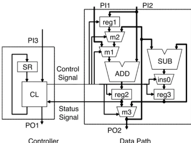
In RTL description, a VLSI circuit generally consists of a controller and a data path. An example of an RTL circuit is shown in Figure 1. A controller consists of a state register (SR) and a combinational logic circuit (CL). SR has a data input and a data output. CL has two data inputs, at most two data outputs, control outputs and status inputs. A datapath consists of primary inputs (PI), primary outputs (PO), hold registers (HR), load registers (LR), multiplexers (MUX), operational modules and observational modules. Each hardware element has at most two data inputs, at most one control input, at most one status output and at most one data outputs.
Each circuit element is connected with signal lines. The signal lines are classified into data signal lines, control sig- nal lines and status signal lines. A data signal line connects a data output to a data input. A control signal line connects a control output of CL to a control input of a hardware ele- ment in the datapaths. A status signal line connects a status output of a hardware element in the datapath to a status in- put of CL.
An RTL circuit is represented as an RTL graph whose vertices are inputs and outputs of hardware elements and whose edges are the signal lines and data flows be- tween inputs and outputs of hardware elements. Let p= (e1,l1,e2, . . . ,ek°1,lk°1,ek) be a path starting from e1and ending at ek. ei and li denote the vertex and the edge, re- spectively. The number of registers on p is called sequen- tial depth of p. p is called a simple path if all ei on p is different. p is called a loop if e1and ekare the same ver- tex and the path from e2to ek°1is a simple path. Different simple paths from ei to ej are called re-convergent paths. If the sink vertex of a path p1 and the source vertex of a path p2 are identical, then we denote the concatenation of the paths as(p1,p2). For inputs and outputs of each hard- ware element on p, the inputs and the outputs are called on-inputsand on-outputs respectively if the inpus and the outputs exist on p. Similarly, the inputs and the outputs are called off-inputs and off-outputs respectively if the inputs and the outputs do not exist on p.
3. Extended-Partially-Strong Testability
In this paper, we define an extended-partially-strong testability for RTL controller-datapath circuits.
Definition 1 (The Range of a Signal Line) A set of val- ues that can appear at a signal line l in normal operation is called the range of l. The range of the input(output) of the hardware element connected with l is defined as the range of line l.
Definition 2 (Dependency) Let Rli and Rl j be the range of signal lines liand lj, respectively. There exists a depen- dency between liat time t and ljat time t0 if lican not be set to any value in Rli at t when lj is set to any value in
m1
reg2 m2 reg1
SR
CL
PO1 PO2
PI1 PI2
PI3
ins0 reg3 ADD
SUB
Status m3 Signal Control Signal
Controller Data Path
Figure 1. An RTL controller datapath circuit. Rli at t0. A dependency between input(output) connected with liand input(output) connected with ljis defined as the dependency between liand lj.
Definition 3 (Extended-partially-strong Testability) Let L be a set of loops in an RTL circuit CD. CD is extended-partially-strongly testable if , for any c 2 L, there exists a simple path pc that satisfies the following conditions.
1. Let pcinbe a simple path from a PI to an on-output of a hardware element mcinon c. Let pcout be a simple path from an on-output of a hardware element mcout on c to a PO. Let pc1be c starting and ending at the on-output of mcin. Let pc2be a simple path from the on-output of mcin to the on-output of mcout along c. Then, pc= (pcin,pc1,pc2,pcout).
2. For any hardware element mion pcin, the on-output of mican be set to any value.
3. For any hardware element mion pcout, there exists a value in the range of the off-input of misuch that the value can propagate any change at the on-input of mi to the on-output of mi.
4. For any hardware element mion pc, let dibe the se- quential depth of the path from the PI on pc to the on-input of mi along pc. There exists no dependency between the PI at time t and the on-input of miat time t+ di.
5. For any two hardware elements mi and mj on pc, let di and dj be the sequential depth of the paths from the PI on pc to the on-input of mi and mj along pc, respectively. If di 6= dj, there exists no dependency between each off-input of mi at time t+ di and each off-input of mjat time t+ dj.
Theorem 1 Let CD be an extended-partially-strongly testable RTL circuit. Let fm be a fault which exists in a hardware element m in CD. Let c be a loop in CD whose the sequential depth is the maximum . Let dpc be the se- quential depth of pc corresponding to c and let nREG be the number of registers in CD. If there exists an input se- quence which can detect fm, a TEM for CD in which fmis
PI
PO 0 1 TC
s1 m1 Controller
ADD1 PI
Figure 2. An exam- ple of the method of [10].
CC TC
Controller
PI
PO 0 1 m1
ADD1 PI
Figure 3. An exam- ple of the proposed method.
detectable can be generated and the number of time frames of the TEM is at most dpc+ nREG.
It is known that ATPGs for combinational circuits can achieve 100% FE in practical test generation time. There- fore, we expect that test generation for the TEM whose the number of time frames is at most dpc+ nREG can achieve 100% FE in practical test generation time.
4. DFT Method
4.1. OverviewIn the proposed DFT method, we first decide control paths from PIs to data inputs of each hardware element and decide observation paths from data outputs of each hard- ware element to POs. In order to propagate any value in the range of each data input by using the control paths and the observation paths, (1)thru functions are added to the hardware elements on the paths and (2) a test controller is added in between normal controller and datapath to control the control signals on the path. Furthermore, if there ex- ists a dependency between inputs of a hardware element by using the paths, the dependency is resolved by using hold functions of registers. Control signals for hold functions are also controlled by using the test controller.
For the control input, the proposed method propagates the value through the normal controller while [10] uses a test controller to provide the value. For the status output of the hardware element, the proposed method also observes any error through the normal controller. Similarly, in order to test CL in the controller, the proposed method utilizes the datapth to propagate any value to the status inputs and to observe any error from the control outputs. Therefore, the complexity of the test controller can be reduced com- pared to [10]. Consequently, the proposed method can re- duce hardware overhead drastically compared to [10]. This is because the extended-partially-strong testability does not require to control and observe any value for the signals be- tween a datapath and a controller but requires to control and observe only any value in the range for them. There- fore, the number of output patterns required for the test controller and the number of MUXs for separating a dat- apath and a controller are decreased and the hardware and delay overheads can be reduced.
An example of the method proposed in [10] and an ex- ample of the proposed DFT method are shown in Figure
2 and 3, respectively. Suppose that MUX m1 exists on a control path (dotted line) for ADD1. In order to propagate values for ADD1 by using the path, the control signal of m1 should be ’0’. Both [10] and the proposed method provide the ’0’ from the test controller. Furthermore, the control input of m1 must be able to be set to both ’0’ and ’1’ for testing m1 itself. In [10], these test patterns for the con- trol input of m1 are also provided from the test controller. Therefore, test MUX s1 is added for switching the control signal from controller to the test controller(Figure 2). On the other hand, in the proposed method, the test patterns for the control input of m1 are provided through the nor- mal controller. Therefore, it is sufficient to provide ’0’ to the control input of m1 and only an AND gate is added in between the controller and the datapath (Figure 3). 4.2. Problem Formulation
We first formulate a DFT problem for making an RTL circuit extended-partially-strongly testable as the following optimization problem.
Definition 4 (DFT for Extended-Partially-Strong Testability )
input: an RTL circuit
output: an augmented RTL circuit which is extended- partially-strongly testable
Optimization: minimizing hardware overhead 4.3. DFT Algorithm
The DFT algorithm consists of the following four steps. 1. Construct a control forest: We construct simple paths from PIs to data inputs of each hardware element. The simple path is called a control path and a set of the simple paths is called a control forest. In order to propagate any value through the control paths, thru functions are added to hardware elements on the path if necessary. Then, we decide the control signals for the hardware elements on the path. From these control signals, a test controller is generated in Step4. When we construct a control forest, we start searching con- trol paths from a PI. Then, we decide a path from the PI to a hardware element. We try to minimize the number of additional thru functions by giving high priority to the hardware elements with thru function for the path selection during the construction of the control forest.
An example of the control forest for Figure 1 is shown in Figure 4. In this example, a thru function is added to SUB. An additional path from PI1 to sreg by the test multiplexer (TM1) is also added.
2. Construct an observation forest: We construct simple paths from the outputs of each hardware element to POs. The simple path is called an observation path and a set of the simple paths is called a observation forest. In order to propagate any error by using ob- servation paths, thru functions are added to hardware elements on the paths if necessary. Then, we decide the control signals for the hardware elements on the paths. From these control signals, a test controller
m1
reg2 m2 reg1
sreg
CL
PO1 PO2
PI1 PI2
PI3
ins0 reg3 ADD
SUB
m3 TM1 ‘0’
‘0’
‘0’
‘1’
‘1’
‘1’ d1
Figure 4. An example of a control forest.
m1
reg2 m2 reg1
sreg
CL
PO1 PO2
PI1 PI2
PI3
ins0 reg3 ADD
SUB
m3 TM1
‘0’,‘1’
d1
Figure 5. An example of an observation forest.
m1 m2 m3 ins0 reg1 reg2 reg3 d1 TM1 TM2
X X 1 X X X X X 1 1
0 0 0 0 1 1 1 1 1 0
0 0 0 0 0 1 1 1 1 0
T T T T 1 1 1 0 0 0
T T T T 1 1 1 0 1 0
T T T T T T T 0 0 X
T : output pattern of the CL X : don’t care
Figure 6. An example of output pat- terns of a test controller.
is generated in Step4. When we construct a observa- tion forest, we start searching observation paths from a PO. Then, we decide a path from the PO to a hard- ware element. We try to minimize the number of ad- ditional thru functions and the required control signals by sharing the control paths and the observation paths as much as possible during the construction of the ob- servation forest.
An example of the observation forest construction for Figure 1 is shown in Figure 5. Additional observation paths from CL to POs are added.
3. Resolve dependencies: If there exist re-convergent paths in the control forest or the observation forest and the sequential depth of the paths are the same, then there exists a dependency between the paths. If there exist dependencies, we decide registers which can resolve the dependencies and the number of the hold cycles to resolve them. The control signals to the registers for resolving the dependencies are pro- vided from the test controller which is generated in Step4. Moreover, the information of the hold cycles is used for the time expansion model generation shown in the next section. In the proposed method, we try to resolve the dependencies by using HRs as much as possible in order to reduce additional hold functions. In Figure 7, a hold function is added to sreg by using test multiplexer TM2.
4. Generate a test controller: We generate a test con- troller(TC) which provides control signals for the con- trol forest, the observation forest and resolving depen- dencies. TC is a combinational hardware element and the output patterns required for TC are selected by ad- ditional PIs. Let n be the number of output patterns of TC, then the number of additional PIs isdlog2ne.TC is inserted between CL and the additional observation paths added in step3. Moreover, the observation paths for the control signals for the additional hardware ele- ments are also added.
An example of the test controller for the RTL circuit in Figure 1 is shown in Figure 6. 1st, 2nd and 3rd lines are the control signals for the control forest, the ob- servation forest and resolving dependencies, respec- tively. 4th and 5th lines are the control signals for
m1
reg2 m2 reg1
sreg
CL
PO1 PO2
PI1 PI2
PI3
ins0 reg3 ADD
SUB
m3 TC
OMUX TM2
TM1 d1
Figure 7. An example of an extended- partially-strongly testable RTL circuit.
the testing of the RTL circuit. 6th line is the con- trol signals for the normal operation. In this example, the number of additional PIs is 3 because the number of the output patterns of the TC is 6. Moreover, by adding the TC, at most 2 gates are inserted between the controller and the data path.
An example of extended-partially-strongly testable RTL circuit is shown in figure 7. To reduce the pin overhead, a MUX (OMUX) is added to the PO in the datapaths to observe the additional observation paths. OMUX is con- trolled with additional PIs.
5. Test Generation Method
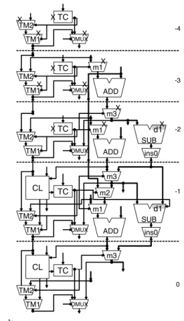
For the test generation of the extended-partially-strongly testable RTL circuit, we generate a time expansion model(TEM) and a combinational ATPG is applied to the TEM. The TEM is generated as follows. First, we gener- ate a TEM that consists of a PO with time frame 0. Then, a hardware element m connected to the PO and the signal line between m and the PO are added to the TEM. When mis added to the TEM for the first time, all the hardware elements connected with inputs of m are added to the TEM. When m which already exists in the TEM is added to the TEM again, only the hardware elements connected on the control forest are added to the TEM. Moreover, all the hard- ware elements which exists on the observation path for m and the corresponding signal lines are also added to the TEM. If m is a register, then only the signal line connected with m is added to the TEM and the time frame is decreased
m1 CL TC m2
TM1 OMUX
m3
d1
-1 -2 -3 -4
SUB ADD ins0
TM2
CL TC
TM1 OMUX
m3
TM2
TC m1
TM1 OMUX
m3
d1 SUB ADD ins0
TM2
TC m1
TM1 OMUX ADD
TM2
TM1 OMUX
TM2
TC
X X
X X
X X
X
X X X
X X
0
X: don’t care
Figure 8. An example of the time expansion model.
by 1. If m is used to resolve the dependencies, the time frame is decreased by the corresponding hold cycles. This process repeats until m becomes a PI and all POs are added to the TEM. An example of the TEM for Figure 7 is shown in Figure 8.
A combinational ATPG is applied to the generated TEM. Then, generated test patterns are transformed so that the test patterns can be applied to the original RTL circuit.
6. Experimental Results
We evaluated the effectiveness of the proposed method by experiments. RTL benchmark circuits used for the ex- periments are GCD, LWF, JWF and PAULIN which are popularly used circuits [10], and RISC and MPEG which are more practical and larger circuits designed by a semi- conductor company [10]. Circuit characteristics of these circuits are shown in Table 1. “#PI” and “#PO” denote the numbers of primary inputs and primary outputs, respec- tively. “#state”, “#FF” and “#Control” denote the num- bers of FFs, status inputs and control outputs, respectively.
“#Reg” and “#Mod.” denote the numbers of registers and the number of hardware elements except for registers, re- spectively. “bit” denotes the bit width of the datapaths.
In our experiments, we used AutoLogicII (Mentor- Graphics) as a logic synthesis tool with its sample libraries to synthesize those circuits. In Table 1, “Area” denotes the
total circuit size. We used TestGen (Synopsys) as a sequen- tial and combinational ATPG tool on Sun Blade 2000 (Sun Microsystems). Test generation for sequential circuits us- ing a TEM requires a combinational ATPG which can deal with multiple stuck-at faults. In this experiments, since TestGen can not deal with multiple stuck-at fault, we use the circuit model which can express multiple stuck-at faults in a time expansion model as single stuck-at fault [14]. We compared the proposed method with original circuits, the full-scan method and the method of [10]. In the full scan method, all the FFs in a circuit is replaced by the scan-FFs and single scan chain is constructed.
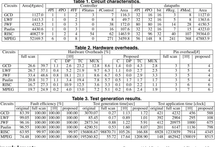
The results of the hardware overhead are shown in Ta- ble 2. “C”, “DP”, “TC” and “MUX” denote the hardware overhead of a controller, a datapath, a test controller and additional MUXs, respectively. The hardware overhead of the proposed method is much smaller than others. Com- pared to [10], we can see that the reduction of the hardware overhead mainly comes from the test controller and the ad- ditional MUXs. Consequently, delay overhead of the pro- posed method is lower than that of [10]. This is because at most 2 gates are inserted in between a controller and a datapath in the proposed method while at most 4 gates are inserted in between them in [10]. We can also observe that pin overhead is smaller than [10].
The results of the test generation are shown in Table 3.
“Test generation time” denotes the time spent for ATPG and does not include the time spent for the DFT. However, the time spent for the DFT is negligible. We observe that the full-scan method, the method of [10] and the proposed method can achieve 100% FE except RISC in practical test generation time. For RISC, the full-scan method and the proposed method cannot generate test vectors for a part of observational modules in the data path. In the results of test application time, the proposed method can achieve much shorter test application time compared with the full-scan method. This is because the proposed method does not re- quire scan-shift operations. Furthermore, full-scan method cannot allow at-speed testing while other approaches can. The proposed method can also achieve much shorter test application time than the method of [10] for five circuits. We consider that faults were efficiently detected by the fault simulation in the proposed method since the whole circuit is the target for test generation while [10] is based on hier- archical test generation.
7. Conclusion
In this paper, we defined the extended-partially-strong testability as a characteristic of RTL controller-datapath circuits. We also proposed a DFT method and a test gener- ation method based on the extended-partially-strong testa- bility. The proposed method achieves 100% FE in practi- cal test generation time by using a combinational ATPG. It also allows at-speed testing. Furthermore, the proposed method can reduce hardware overhead and test application time drastically compared with [10] .
Table 1. Circuit characteristics.
Circuits Area[#gates] Controller datapaths
#PI #PO #FF #Status #Control Area #PI #PO bit #Reg. #Mod. Area
GCD 1127.0 1 1 2 3 7 116.3 32 16 16 3 8 1127.0
LWF 1413.3 1 0 2 0 8 49.7 32 32 16 5 8 1363.6
JWF 4322.5 1 0 3 0 38 172.0 80 80 16 14 28 4150.5
Paulin 4430.6 1 0 3 0 16 107.6 32 32 16 7 15 4323.0
RISC 40827.9 1 2 4 54 62 1463.9 32 96 32 40 107 39364.0
MPEG 52169.5 6 0 8 0 271 3459.8 56 148 8 241 368 47883.9
Table 2. Hardware overheads.
Circuits Hardware Overheads [%] Pin overhead[#]
full scan [10] Proposed full scan [10] proposed
C DP TC MUX C DP TC MUX
GCD 26.6 39.7 1.1 2.6 23.2 12.8 8.6 1.4 0.0 4.3 2.8 3 5 4
LWF 26.7 37.1 0.4 5.2 21.9 9.7 6.3 1.1 0.0 2.7 2.5 3 5 4
JWF 33.4 48.6 0.8 18.1 21.1 8.6 6.7 0.5 0.0 2.9 3.3 3 5 4
Paulin 20.8 31.7 1.1 3.4 19.4 7.8 5.7 0.5 1.7 1.7 1.7 3 5 4
RISC 16.7 27.3 0.1 10.9 12.5 3.6 3.3 0.1 0.0 2.2 1.1 3 6 6
MPEG 19.7 24.9 0.2 4.0 13.0 7.2 5.1 0.2 0.6 2.4 1.9 3 7 6
Table 3. Test generation results.
Circuits Fault efficiency [%] Test generation time[sec] Test application time [clock] original full scan [10] proposed original full scan [10] proposed original full scan [10] proposed
GCD 83.39 100.00 100.00 100.00 3070.07 0.27 1.13 1.72 421 4232 456 588
LWF 99.05 100.00 100.00 100.00 85.45 0.17 0.89 1.01 392 2904 295 108
JWF 96.16 100.00 100.00 100.00 2873.34 0.88 1.22 5.91 412 20975 1000 675
Paulin 96.55 100.00 100.00 100.00 4290.51 0.53 1.60 8.07 201 6147 1136 798
RISC 63.95 99.97 100.00 99.97 156808.67 98870.71 105.26 166.88 6928 1233859 7914 4345 MPEG 74.48 100.00 100.00 100.00 195260.82 55.72 17.64 1208.90 148 462942 150019 8515
Acknowledgments
The authors would like to thank Profs. Michiko In- oue and Satoshi Ohtake of Nara Institute of Science and Technology for their valuable discussions. This work was supported in part by 21st Century COE Program and in part by Japan Society for the Promotion of Sci- ence (JSPS) under Grants-in-Aid for Scientific Research B(2)(No. 15300018).
References
[1] H. Fujiwara, Logic Testing and Design for Testability, The MIT press, 1985.
[2] T. Inoue, D. K. Das, T. Mihara, C. Sano and H. Fujiwara,
“Test generation for acyclic sequential circuits with hold registers,” International Conference on Computer Aided De- sign, pp.550-556, Nov. 2000.
[3] M. Abramovici, M. A. Breuer and A.D.Friedman, Digi- tal Systems Testing and Testable Design, Computer Science Press, 1990.
[4] S. Dey and M. Potkonjak, “Non-scan design-for-testability of RT-level data paths,” in Proc. Int. Conf. Computer-Aided Design, pp.640-645, Nov.1994.
[5] R. B. Norwood and E. J. McCluskey, “Orthogonal scan:Low overhead scan for Data Paths,” Proc.1996 Int.Test Conf.,pp.659-668, 1996.
[6] R. B. Norwood and E. J. McCluskey, “High-level synthesis for orthogonal scan,” Proc. 15th VLSI Test Symp, pp370- 375, 1997
[7] J. Lee and J.H. Patel, “Hierarchical test generation under architectural level functional constraints,” IEEE Trans. on
Computer-Aided Design of Integrated Circuits and Systems, vol. 15, no. 9, pp. 1144-1151, Sept. 1996.
[8] I. Ghosh, A. Raghunathan, and N. K. Jha, “Design for hi- erarchical testability of RTL circuits obtained by behav- ioral synthesis,” Proc. IEEE. Int. Conf. on Computer Design, pp.173-179, 1995
[9] I. Ghosh, A. Raghunathan, and N. K. Jha, “A Design for Testability Techique for RTL Circuits Using Control/Data Flow Extraction,” IEEE Trans. on Computer Aided Design, Vol.17, pp.706-723, Aug.1998.
[10] S. Ohtake, H. Wada, T. Masuzawa and H. Fujiwara, ”A non- scan DFT method at register-transfer level to achieve com- plete fault efficiency,” Proc. Asia and South Pacific Design Automation Conference 2000, pp.599-604, 2000.
[11] S. Ohtake, T. Masuzawa and H. Fujiwara, “A non-scan DFT method for controllers to achieve complete fault efficiency,” in Proc. of the 7th Asian test symposium, pp.204-211,1998. [12] H. Wada, T. Masuzawa, K. K. Saluja and H. Fujiwara, “De-
sign for strong testability of RTL data paths to provide com- plete fault efficiency,” Proc. of 13th International Conf.on VLSI Design, pp.300-305, Jan. 2000.
[13] Hiroyuki Iwata, Tomokazu Yoneda, Satoshi Ohtake, and Hideo Fujiwara, “A DFT Method for RTL Data Paths Based on partially strong testability to Guarantee Complete Fault Efficiency,” in Proc. of the 14th Asian Test Symposium, pp. 306-311, Dec. 2005.
[14] H. Ichihara, and T. Inoue, “A method of test generation for acyclic sequential circuits using single stuck-at fault combi- national ATPG,” IEICE Trans. Fundamentals, Vol. E86-A, No. 12, pp. 3072-3078, Dec. 2003.