Fast False Path Identification Based on Functional Unsensitizability
Using RTL Information
∗Yuki Yoshikawa
1, Satoshi Ohtake
2, Tomoo Inoue
1and Hideo Fujiwara
21
Graduate School of Information Science, Hiroshima City University
3-4-1 Ozuka-higashi, Asaminami, Hiroshima 731-3194, Japan
2
Graduate School of Information Science, Nara Institute of Science and Technology
Kansai Science City 630-0192, Japan
E-mail:
1{yosikawa, tomoo}@hiroshima-cu.ac.jp,
2{ohtake, fujiwara}@is.naist.jp
AbstractIn this paper, we propose a method for identifying false paths based on functional unsensitizability of path delay faults. By using RTL structural information, a number of gate level paths are bound into an RTL path and the bun- dle of them can be identified in a reasonable amount of time. The identified false paths are useful for over-testing reduc- tion caused by DFT techniques, such as scan design, and also area and performance optimization of circuits during logic synthesis. Experimental results show that our proposed method can identify false paths in a few seconds for several benchmarks.
1. Introduction
In recent years, digital systems are widely used, and thus high performance LSIs are strongly required. Delay test- ing is significantly important to ensure that a given circuit behaves correctly at a desired system clock. In addition, accurate delay estimation of a circuit is also important for decision of the circuit performance. In general, it is said that there are a number of false paths in a circuit[1]. False paths induce some severe problems such as over-testing of delay faults and inaccurate estimation of a system clock pe- riod. False path identification contributes to the alleviation of those problems. In this paper, we propose a method of identifying false paths using register transfer level (RTL) in- formation while most of the previous methods were done at gate level.
Several methods of untestable path identification have been proposed in the last decade. As gate-level approaches, the techniques presented in [1, 2, 3] identify untestable paths for combinational circuits. The works for sequential cir- cuits [4, 5] are equally important. Works in [6, 7] proposed methods to identify multi-cycle paths at gate-level. How- ever, gate-level approaches would consume long CPU time for dealing with the large number of gate-level paths. As
∗This work was supported in part by Semiconductor Technology Aca- demic Research Center under Research Project.
an approach from higher level of abstraction, the work in [8] proposed a method for eliminating false paths at RTL and contributed to prevention of inaccurate delay estimation. Note that the work does not list the identified false paths at gate-level and does not deal with shorter false paths than the critical path.
In the work [9], a method for identifying non-robust untestable (NRU) paths focusing on data transfer of a cir- cuit have been proposed. In the work, paths are dealt with at RTL, called RTL paths [10]. An RTL path is a bundle of gate-level paths between two registers. The total num- ber of RTL paths in a circuit is much smaller than that of its gate-level paths, and therefore the identification for even an industrial circuit can be done in a reasonable amount of time. However, the identified NRU paths are useful for over- testing reduction under single fault assumption only. This is because the delay on an NRU path does not affect the circuit performance unless the NRU path is affected by a delay on another path. Note that an NRU path still includes a func- tionally sensitizable path. Thus, if we relax the single fault assumption, that is, if we consider more realistic environ- ment, due to over-testing reduction, eliminating path delay faults (PDFs) on the identified NRU paths from the target of testing will miss defects that cause multiple PDFs.
In this paper, we will show a sufficient condition for iden- tifying functionally unsensitizable (FU) paths focusing on RTL structure and data transfer information. Since an RTL path in an RTL circuit corresponds to a bundle of gate-level paths in its synthesized circuit, we can identify bundles of FU paths, which are false paths, by means of the sufficient condition. The identified false paths support accurate over- testing reduction (high quality delay testing) compared to NRU paths identified by the method in [9]. Furthermore, as an advantage of false path identification at RTL, the RTL paths that are identified as false can be used for area and per- formance optimization during logic synthesis.
2. Overview
Our path identification method is applied to structural RTL designs. If a target RTL circuit is described as a func-
0 1 0 1 R1
R3
s0 s1 s2
s0 s1
s2 add
R2 R4
CR1 CM1
PI1 PI2
M1
Controller
Status signals Control signals
CR3
M2
PI3
cmp CR5 R5
PO1 PO2
M3
p1 P
2
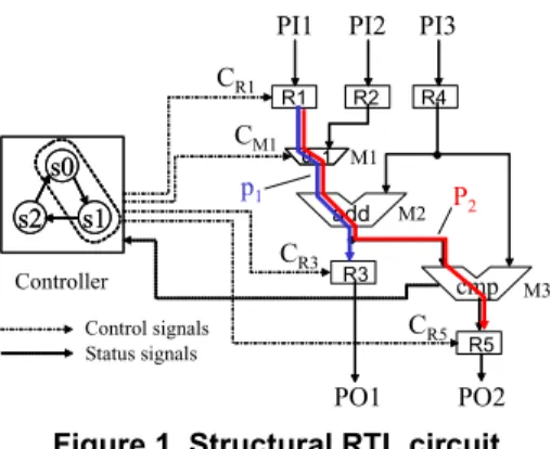
Figure 1. Structural RTL circuit.
tional RTL, we can extract the structural information dur- ing synthesis process. For example, Explorations tool[11], which is a high-level synthesis tool, can generate a struc- tural RTL from its original functional RTL. An example of a structural RTL circuit is shown in Figure 1. A structural RTL design consists of a controller represented by a finite state machine, a datapath represented by RTL modules such as MUXs, operational modules and registers, and RTL sig- nal lines between them. For convenience, fan-out branches on RTL signal lines are treated as RTL modules. The con- troller provides control inputs to the RTL modules. On the other hand, the status signals from the datapath are fed to the controller to determine state transitions.
Here let us consider the difference between FU path and NRU path identification at RTL using Figure 1 and 2. Figure 2 shows the state transition table of the con- troller in Figure 1. Let p1="R1,MU X,ADD,R3# and p2="R1,MU X,ADD,CMP,R5# be target RTL paths. Our path identification takes interest in control signals at every state transition. For p1, CR1at S0 is load, CM1 at S1 is zero (CM1 is selecting p1) and CR3 at S1 is load. This means that there exists a state transition where a transition at R1 is launched at the first state and is propagated along p1at the next state and finally captured into R3. Therefore we do not identify p1as neither FU nor NRU paths at RTL.
On the other hand, p2is identified as NRU because, for the state transition S0→ S1, CR5at S1 is Hold (not captured), for S1→ S2, CM1at S2 does not select p2(not propagated) and for S2→ S0, CR1at S2 is Hold (not launched). This im- plies that, for all the state transitions, there is no case where the event at R1 is launched, propagated along p2and cap- tured into R5 under single fault assumption (delay exists on the target path p2only). It should be noted that p2is not FU because CR1, CM1and CR5can also have delay under multiple fault assumption, and accordingly the delay on p2is observ- able due to the outside delays if any. Therefore p2is not FU and it should not be excluded from the target of testing. If the delay on p2 is not observable regardless of the outside delays, p2is FU, that is false.
Since we identify false paths at RTL, it is necessary to clarify the correspondence between RTL paths and gate-level paths. In this paper, to achieve the clarification, we con-
PS: Present state, NS: Next state,
R : Reset, Load enable ‘1’ is Load, ‘0’ is Hold 0011
S0 S0 S2
1100 S0
S2 S1
1110 S0
S1 S0
(CR1, CR3, CR5, CM1) R=1
R=0
Output vector NS
PS
0011 S0
S0 S2
1100 S0
S2 S1
1110 S0
S1 S0
(CR1, CR3, CR5, CM1) R=1
R=0
Output vector NS
PS
Figure 2. State transition table.
sider a module interface preserving-logic synthesis (MIP- LS). Given an RTL circuit, an MIP-LS transforms each RTL module and each RTL signal line into its own gate-level netlist and single-bit signal lines, respectively. During an MIP-LS for an RTL circuit, optimization is performed within each module, and each RTL signal line connecting RTL modules is just split to single-bit signal lines. Therefore, the connectivity of all the RTL modules in the RTL circuit is guaranteed to be propagated to a synthesized gate-level circuit through any MIP-LS. For example, a logic synthesis tool DesignCompiler (Synopsys) is able to run MIP-LS with default setting unless the flatten option is set. In the near fu- ture, MIP-LS like logic synthesis may be useful if several test approaches come to be applied at higher-level of design ab- straction. If we suppose a logic synthesis without preserving boundary of each RTL module, it may be hard to completely establish the correspondence although circuit area and per- formance can be optimized. The work for any logic synthe- sis with no constraints is our future work.
Experimental results show that our proposed method can identify false paths in a few seconds for several benchmark circuits.
3. RTL-FU path identification 3.1. Gate level FU path
A path p in a combinational circuit is an ordered set of gates(g0,gi, ...,gn) where gi(1 ≤ i ≤ n − 1) is a gate, and g0 and gn are a primary input and a primary output, re- spectively. The output of giconnects with an input of gi+1
(0 ≤ i ≤ n − 1). The testability of a path is classified into four types: robustly testable, non-robustly testable, function- ally sensitizable and functionally unsensitizable[12]. This classification is based on the possibility of transition made at on-inputs and off-inputs on the path under consideration by input vector pairs. For an input of a gate gi in path p, if the input is included as a connection(gi−1,gi) composing the path p, the input is said to be an on-input , otherwise the input is said to be an off-input. By the formal definition of path delay faults (PDFs), a path is functionally unsensitiz- able (FU) if it is none of robust testable, non-robust testable and functionally sensitizable paths. Intuitively, a path is FU if any transition occurring at the primary input of the path does not affect the end of the path or the primary output even though any unexpected delays occur at the off-inputs.
In this paper, we consider path delay faults in sequential
circuits, especially single-cycle delays, i.e., even if a logic circuit has an extra delay, the delay is at most one cycle over and less than two cycles. Note that, in case of sequential cir- cuits, the start and end points can be flip-flops (FFs). There- fore, transition on a path from cycle t to t+ 1 in a sequential circuit depends not only on the change of the content in the start FF, but also on a load-enable signal applied at the previ- ous cycle t− 1 from the controller. Thus, in order to identify FU paths in sequential circuits, it is important to consider the control signals for FFs as well as the condition on off-inputs.
3.2. RTL-FU path
In this section, by developing the concept of gate-level FU paths, here we discuss the functionally unsensitizabil- ity of RTL paths. An RTL path is an ordered set of RTL modules"Rs,M1,M2, ..,Mn,Re#, where Rs is a register or a primary input, Re is a register or a primary output. Also Mi(1 ≤ i ≤ n) is a combinational RTL module and the output of Miconnects with an input of Mi+1. We define an RTL-FU path as follows.
Definition 1 (RTL-FU path) An RTL path p in an RTL cir- cuit is RTL-FU if all gate-level paths corresponding to p in its gate-level circuit are gate-level FU for any logic synthesis.
!
An RTL path p is RTL-FU if p satisfies at least one of the following four properties at any consecutive two cycles t and t+ 1.
1. No transition is launched at the output of the start reg- ister Rs in cycle t irrespective of the delay of the load- enable signal applied to Rs and/or input data delivered to Rs in the cycle t.
2. Even if a transition is launched at Rs, it never reaches the end register Re along p in cycle t+ 1 irrespective of the delay of the off-inputs, which include control sig- nals applied to the RTL modules Mi, on p.
3. The reached value is never captured into Re in cycle t+ 1 irrespective of the delay of the load-enable signal applied to Re.
4. The captured value of Re at cycle t+ 1 never affects any PO at the latter cycles irrespective of the delay of the off-inputs of RTL modules on all the propagation paths from Re to any PO.
3.3. Control-dependent FU path
In this section, we show a sufficient condition of RTL- FU path focusing on the load-enable signals of registers and the select signals of MUXs. An RTL-FU path identified by the sufficient condition is said to be a control-dependent FU (CFU) path. We distinguish RTL paths starting at the SR from other RTL paths. By considering state assignment, we can know the time when transitions are launched for each bit of the SR and the directions of the transitions. Therefore we take the information about the state assignment and the directions of the transitions into account when identifying
RTL-FU paths starting at the SR. A register in a datapath is referred to as a datapath register (DR).
3.3.1. RTL path starting at DR/PI
In the following discussion, we focus on start and end registers and MUXs on RTL paths. Thus, an RTL path p is expressed as a sequence of registers Rs, Re and MUXs Mi(1 ≤ i ≤ n), where n is the number of MUXs on p, i.e., p="Rs,M1,M2, ..,Mn,Re#. Let CtRbe load-enable signals of R in cycle t. If the load-enable signal of a register is ’1’, the register loads a value, otherwise it holds its value. Note that if a register has no hold function or the starting point of a path p is a PI or the ending point of p is a PO, we assume that the PI and PO are registers with no hold function, and each of the registers has a load-enable signal and it is always
’1’. Let CtM
i be the select signal of Miin cycle t. When Mi
selects the input side on p, the value of the select signal is denoted as pMi. For example, suppose that p is the RTL path
"R1,M1,ADD,R3# in Figure 1. When M1selects p at cycle t, CMt
1=pM1=0.
We first consider functional uncontrollability and func- tional unobservability of registers. If a register is function- ally uncontrollable at cycle t, the captured value at cycle t is the same as that at cycle t− 1 although the register loads a value at cycle t. Thus, the register has no transition at cycle t. If a register is functionally unobservable at cycle t, the cap- tured value at cycle t is not propagated to any primary output at any cycle.
Definition 2 (Functional uncontrollability of register) Suppose a register R, and let P be a set of RTL paths whose end register is R. Register R is functionally uncontrollable at cycle t if for any RTL path p∈ P,
• for each MUX Mion p, CtM
i= C
t−1
Mi = CMt−2i (1 ≤ i ≤ n), where n is the number of MUXs on p, and
• if for each Mi on p, CtM
i = pMi(1 ≤ i ≤ n), then the start register Rs of p satisfies Ct−1R
s = C
t−2
Rs = 0, or Rs is functionally uncontrollable at cycle t− 1. ! Definition 3 (Functional unobservability of register) Suppose a register R, and let P be a set of RTL paths whose start register is R. Register R is functionally unobservable at cycle t if both of the following two conditions are satisfied.
• For any RTL path p ∈ P,
– for each Mion p, there exists Misuch that CMt
i̸=
pMi∧Ct+1Mi ̸= pMi, or
– for the end register Re of p, CtRe= CRet+1= 0 or Re is functionally unobservable at cycle t+ 1.
• If for the register R, CRt+1= 0, then R is also functionally unobservable at cycle t+ 1.
Theorem 1 An RTL path p is RTL-FU if at least one of the following three conditions is satisfied for any state transition from cycle t to t+ 1.
Condition 1: (1) For the start register Rs, Ct−1Rs = CtRs= 0 or (2) Rs is functionally uncontrollable at cycle t.
Condition 2: For each Mi on p, there exists Mi such that
0 1 + RTL path p
( H, H, * ) ( *, *, * )
( *, *, * )
0 1 + (*, L, * )
(*, 1, 1 )
(*, *, * )
0 1
Re + (*, L, * ) (*, *, 0 )
(*, H, H ) Condition 1 (1)
Rs Rs Rs
Re Re
Condition 2 Condition 3 (1) (*, *, *): Each control signal at time t-1, t, t+1
H: Hold, L: Load, *: H or L or 0 or 1
Figure 3. Examples of Conditions 1(1), 2, and 3(1) in Theorem 1 at some cycle t and t+ 1. CtM
i̸= pMi∧C
t+1 Mi ̸= pMi.
Condition 3: (1) For the end register Re, CtRe= Ct+1Re = 0 or (2) Re is functionally unobservable at cycle t+ 1. ! The sketch of the proof of Theorem 1 is as follows. Suppose a state transition of a controller. If Condition 1 in Theorem 1 is satisfied for the state transition, no transition is launched at any FF that corresponds to Rs even if the load-enable sig- nal line has delay. If Condition 2 in Theorem 1 is satisfied for the state transition, propagation of any transition on any gate-level path corresponding to p is prevented even if the select signal of a MUX has delay. If Condition 3 in The- orem 1 is satisfied for the state transition, no transition is captured at any FF that corresponds to Re even if the load- enable signal line has delay, or the captured value at the FF is never observed at any PO. For any state transition, if at least one of the three conditions in Theorem 1 is satisfied, all the gate-level paths corresponding to p are FU. Therefore, p is RTL-FU if Theorem 1 is satisfied.
Conditions 1(1), 2 and 3(1) in Theorem 1 show the con- ditions of control signals for three cycle t− 1, t and t + 1. Examples of them are shown in Figure 3. The three-tuple of each parenthesis in Figure 3 shows control signal values of each register or MUX at cycle t− 1, t and t + 1. For Con- dition 1(1), Rs holds a value at cycle t− 1 and t. Thus, no transition is launched at Rs at cycle t even if the load-enable signal line has delay. For Condition 2, the MUX on p does not select p at cycle t and t+ 1. Thus, no transition at the starting point of p is propagated to the ending point along p at cycle t+ 1 even if the control signal line has delay. For Condition 3(1), Re holds a value at cycle t and t+ 1. Thus, no transition at Rs is ever captured into Re at cycle t+ 1 even if the load-enable signal line has delay.
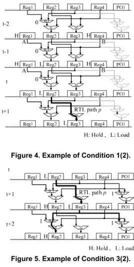
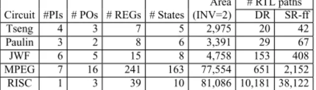
Conditions 1(2) and 3(2) are the conditions for the up- stream and downstream of the path, respectively. Condition 1(2), concerning the uncontrollability, is that the captured value of Rs at cycle t is the same as the previous value of Rs even if the load-enable signal of Rs is ‘load’ at cycle t; that is, there is no transition at Rs. Condition 3(2), concerning the unobservability, is that the captured value of Re at cycle t+ 1 is not propagated to any PO even if the load-enable signal of Re is ‘load’ at cycle t+ 1. We show examples of these con- ditions in Figures 4 and 5, which are time expansion models of an RTL circuit.
Figure 4. Example of Condition 1(2).
Figure 5. Example of Condition 3(2).
In Figure 4, the target RTL path p is Reg2-Sub-Reg3. Reg2 loads a new value ’A+B’ at cycle t. However, the value is the same as the previous value that Reg2 loaded at cy- cle t− 1 because the select signal of the MUX is the same at cycle t, t− 1 and t − 2. Moreover, Reg1 and Reg4 hold their values at cycle t− 1 and t − 2. This is one of the cases where Condition 1(2) is satisfied. If a control signal of a source register at cycle t− 1 is ‘load’, we will recursively check whether the value captured into the source register is the same as the previous one.
In Figure 5, the target RTL path p is Reg2-MUX-Add- Reg3. The transition launched at Reg2 is captured to Reg3 at cycle t+ 1. However, the value cannot propagate to any PO because Reg1 holds a value at cycle t+ 1 and t + 2. If Reg1 captures the value, we will recursively check the next time frame at cycle t+ 3. For the other path from Reg3 to PO1, since the MUX on the RTL path does not select the path at t+ 1 and t + 2, propagation of the value is prevented by the MUX.
3.3.2. RTL paths starting at SR-ff
For RTL paths from flip-flops in the SR (SR-ff), Theorem 1 can also be applied. The SR in a controller uploads a new
value every clock cycle. It means that CRs always becomes 1 (load). Therefore RTL paths from the SR-ff to DRs do not satisfy Condition 1 (1) in Theorem 1. Here we consider transitions from each SR-ff. The relation between states and values of the flip-flops is determined by state assignments. We can obtain the information on state assignments during logic synthesis or designers can also determine state assign- ments before logic synthesis. From the information on state assignments and state transition, we can know the time when a transition is launched at each flip-flop. For example, let us consider state assignments to the controller in Figure 1. We assume that the SR in the controller consists of two flip-flops (FF0,FF1), and (0,0), (0,1) and (1,1) are assigned to S0, S1and S2, respectively. When S0transfers to S1, FF1 has a rising transition.
An RTL path is FU with respect to a rising (resp. falling) transition if at least one of the three conditions in Theorem 1 is satisfied for all the time t when a rising (resp. falling) transition is launched at the SR-ff of the starting point of the RTL path. Moreover, if an RTL path is FU w.r.t. both rising and falling transitions, the RTL path is FU.
4. Experimental results
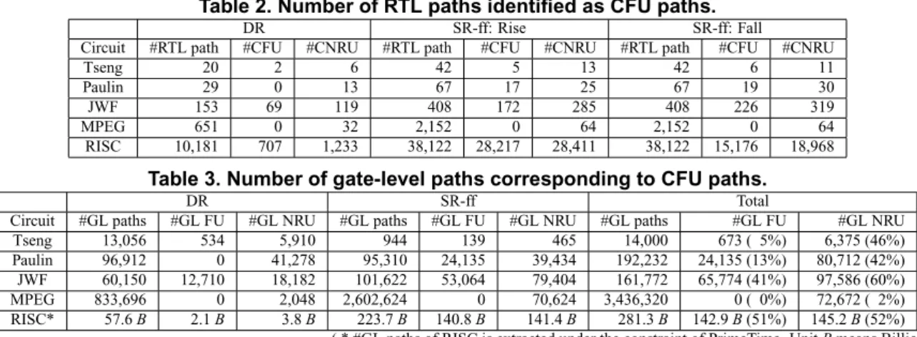
In this section, we evaluate the effectiveness of identify- ing control-dependent FU (CFU) paths for some RTL bench- mark circuits. The circuit characteristics are shown in Ta- ble 1. Tseng[13], Paulin[14] and 4th Jaumann Wave Filter (JWF)[15] are widely used RTL benchmark circuits. MPEG and RISC processor1are provided by industry. The first six columns show circuit name, the numbers of PIs, POs, reg- isters and states of the controller, and the total area of the circuit, respectively. Logic synthesis is performed by De- signCompiler (Synopsys) with TSMC 0.18µm compatible li- brary provided by Oklahoma State University[16]. The last two columns show the number of RTL paths. Column DR shows the numbers of RTL paths that starts at a datapath reg- ister or a PI and Column SR shows the number of RTL paths that starts at an FF in the state register.
Table 2 shows the number of RTL paths identified as CFU by our proposed method. The second column under DR shows the number of RTL paths starting at DRs. The third column shows the number of RTL paths identified as CFU among the RTL paths in the second column. For JWF, 69 of 153 RTL paths were identified as CFU. For RISC, 707 of 10,181 RTL paths were identified as CFU. On the other hand, MPEG has many registers with no hold function. Thus, most starting registers launch transitions and most ending registers capture propagated transitions in every clock cycle. There- fore there was no RTL path identified as CFU. We suppose MPEG has few false paths.
For each of all the benchmark circuits except for RISC,
1These circuits were provided for the Joint Research (1997-2001) with Semiconductor Technology Academic Research Center (STARC).
Table 1. Circuit characteristics of benchmarks.
Area # RTL paths Circuit #PIs # POs # REGs # States (INV=2) DR SR-ff
Tseng 4 3 7 5 2,975 20 42
Paulin 3 2 8 6 3,391 29 67
JWF 6 5 15 8 4,758 153 408
MPEG 7 16 241 163 77,554 651 2,152
RISC 1 3 39 10 81,086 10,181 38,122
the CPU time required for identifying CFU paths is less than 1 second. Even for RISC that has the huge number of paths, the CPU time is less than 10 seconds. The third col- umn shows the number of RTL paths identified as control- dependent non-robust untestable (CNRU)[9]. All the gate- level paths corresponding to the CNRU paths are non-robust untestable. The work[9] proposed a method for identifying CNRU paths at RTL and we applied the method to this exper- iment. The number of identified CFU paths is less than that of identified CNRU paths because the class of CFU paths is properly included in the class of CNRU paths. The next three columns and the last three columns show results for RTL paths starting at SR-ffs with rising transitions and starting at SR-ffs with falling transitions, respectively. For each circuit except for MPEG, a number of RTL paths were identified as CFU. Especially, for JWF and RISC, many RTL paths were identified as CFU.
Table 3 shows the number of gate-level paths cor- responding to the identified CFU paths and CNRU paths at RTL, respectively. We extracted gate-level paths using PrimeTime (Synopsys). For Tseng, Paulin, JWF and MPEG, we extracted all the gate-level paths in each circuit. For RISC, we extract gate-level paths under the constraint where PrimeTime can deal with up to two million paths between two FFs specified by a user. The suffix B means billion. The second, fifth and eighth columns show the numbers of gate-level paths starting at DRs, SR-ffs and their total, re- spectively. The third column shows the number of gate-level paths corresponding to the identified CFU paths starting at DR and the sixth column shows the sum of gate-level paths corresponding to the identified CFU paths starting at SR-ffs with rising or falling transitions. The ninth column shows their total number and these paths are gate-level FU paths (false paths) which were identified by our proposed method. From the results, 142.9 billion of 281.3 billion paths (51%) were identified as false within 10 seconds for RISC. For JWF and Paulin, 65,774 and 24,135 paths were identified as false with 1 second, respectively.
On the other hand, a sequential ATPG algorithm can iden- tify FU path delay faults (PDFs) at gate-level. However, common sequential ATPG tools do not support the fault class of FU. To show the speedup of the proposed method, we evaluated the run time required for identifying NRU PDFs by using the sequential ATPG tool, TetraMax. For both JWF and Paulin, TetraMax took about 50 hours to identify 10,000 NRU PDFs. It is conceivable that there is no large difference between the complexity of NRU PDFs identification and that of FU PDFs identification. Therefore, our method achieved
Table 2. Number of RTL paths identified as CFU paths.
DR SR-ff: Rise SR-ff: Fall
Circuit #RTL path #CFU #CNRU #RTL path #CFU #CNRU #RTL path #CFU #CNRU
Tseng 20 2 6 42 5 13 42 6 11
Paulin 29 0 13 67 17 25 67 19 30
JWF 153 69 119 408 172 285 408 226 319
MPEG 651 0 32 2,152 0 64 2,152 0 64
RISC 10,181 707 1,233 38,122 28,217 28,411 38,122 15,176 18,968
Table 3. Number of gate-level paths corresponding to CFU paths.
DR SR-ff Total
Circuit #GL paths #GL FU #GL NRU #GL paths #GL FU #GL NRU #GL paths #GL FU #GL NRU
Tseng 13,056 534 5,910 944 139 465 14,000 673 ( 5%) 6,375 (46%)
Paulin 96,912 0 41,278 95,310 24,135 39,434 192,232 24,135 (13%) 80,712 (42%)
JWF 60,150 12,710 18,182 101,622 53,064 79,404 161,772 65,774 (41%) 97,586 (60%)
MPEG 833,696 0 2,048 2,602,624 0 70,624 3,436,320 0 ( 0%) 72,672 ( 2%)
RISC* 57.6 B 2.1 B 3.8 B 223.7 B 140.8 B 141.4 B 281.3 B 142.9 B (51%) 145.2 B (52%) ( * #GL paths of RISC is extracted under the constraint of PrimeTime. Unit B means Billion)
great success in reduction of the run time required for false path identification by using RTL information.
There is another benefit of using identified false path. By eliminating the identified false paths from the target of test- ing, over-testing of delay faults caused by DFT is reduced. For JWF, 65,774 paths were identified as false, on the other hand, 97,586 paths were identified as NRU by the method proposed in [9]. If we exclude the identified 97,586 NRU paths from the target of testing, we will miss some delay defects that induce multiple PDFs because some PDFs on 31,812 (97,586-65,774) paths are functionally sensitizable. Therefore, we should exclude PDFs only on 65,774 paths to prevent miss of such defects.
We are interested in how effective using the identified false paths is with respect to area and performance optimiza- tion during logic synthesis. Utilization of the identified false paths and evaluation of this are our future works.
5. Conclusion
In this paper, we presented a method for identifying false paths focusing on the RTL structure and the data transfer of a circuit. Our experimental results showed that a large num- ber of false paths were found by identifying RTL-FU paths. The time required for the identification was less than a few seconds for all the benchmark circuits. The information of identified false paths is useful for over-testing reduction and test accuracy improvement. It is conceivable that using the information is also efficient for optimization of circuit area and performance during logic synthesis. Evaluating the ef- fectiveness of using the identified false paths information is our future work.
Acknowledgment
The authors would like to thank Profs. Michiko Inoue and Tomokazu Yoneda of Nara Institute of Science and Tech- nology for their valuable discussion and their cooperation. This work was supported in part by Semiconductor Tech- nology Academic Research Center (STARC) under Research Project, and in part by Japan Society for Scientific Research (B) (No.20300018)
References
[1] K.T. Cheng and H.C. Chen, “Classification and identification of non- robust untestable path delay faults,” IEEE Trans. Computer-Aided De- sign of Integrated Circuits and Systems, vol.15, no.8, pp.854–853, Aug. 1996.
[2] S. Kajihara, K. Kinoshita, I. Pomeranz, and S.M. Reddy, “A method for identifying robust dependent and functionally unsensitizable paths,” Proc. International Conf. on VLSI Design, pp.82–87, 1997. [3] S.M. Reddy, S. Kajihara, and I. Pomeranz, “An efficient method to
identify untestable path delay faults,” Proc. 10th IEEE Asian Test Symp., pp.233–238, 2001.
[4] A. Krstic, S.T. Chakradhar, and K.T. Cheng, “Testable path delay fault cover for sequential circuits,” Proc. European Design Automa- tion conf., pp.220–226, 1996.
[5] R. Tekumalla and P.R. Menon, “Identifying redundant path delay faults in sequential circuits,” Proc. 9th International Conf. VLSI De- sign, pp.406–411, 1996.
[6] W.C. Lai, A. Krstic, and K.T. Cheng, “On testing the path delay faults of a microprocessor using its instruction set,” Proc. 18th VLSI Test Symp., pp.15–20, 2000.
[7] K. Yang and K.T. Cheng, “Efficient identification of multi-cycle false path,” Proc. 11th Asia and South Pacific Design Automation Conf., pp.360–365, 2006.
[8] M. Nourani and A. Papachristou, “False path exclusion in delay anal- ysis of RTL structures,” IEEE Trans. on VLSI Systems, vol.10, no.1, pp.30–43, Feb. 2002.
[9] Y. Yoshikawa, S. Ohtake, and H. Fujiwara, “False path identification using RTL information and its application to over-testing reduction for delay faults,” Proc. 14th Asian Test Symp., pp.65–68, 2007. [10] M.A. Amin, S. Ohtake, and H. Fujiwara, “Design for hierarchical two-
pattern testability of data paths,” IEICE Trans. on Information and Systems, vol.E85-D, no.6, pp.975–984, Jun. 2002.
[11] Y Explorations, Inc., Explorations tool, http://www.yxi.com/index.html.
[12] A. Krstic and K.T. Cheng, Delay Fault Testing for VLSI Circuits, Kluwer Academic Publishers, 1998.
[13] C.J. Tseng and D.P. Siewiorek, “Automated synthesis of datapaths in digital systems,” IEEE Trans. Computer-Aided Design of Integrated Circuits and Systems, vol.5, no.3, pp.379–395, July 1986.
[14] P.G. Paulin and J.P. Knight, “Force directed scheduling for the be- havioral synthesis of asics,” IEEE Trans. Computer-Aided Design of Integrated Circuits and Systems, vol.8, no.6, pp.661–679, June 1988. [15] T. Takasaki, T. .Inoue, and H. Fujiwara, “A high-level synthesis ap-
proach to partial scan design,” Proc. 8th IEEE Asian Test Symp., pp.309–314, 1999.
[16] J.E. Stine, J. Grad, I. Castellanos, J. Blank, V. Dave, M. Prakash, N. Iliev, and N. Jachimiec, “A framework for high-level synthesis of system-on-chip designs,” IEEE Computer Society, International conf. on Microelectronic Systems Education, pp.11–12, 2005.