An Optimal Time Expansion Model Based on Combinational ATPG
for RT Level Circuits
Tomoo Inoue+, Toshinori Hosokawat, Takahiro Miharat, and Hideo Fujiwara+
+ Graduate School of Information Science Nara Institute of Science and Technology Takayama, Ikoma, Nara 630-0101, Japan
8 Corporate Semiconductor Development Division Matsushita Electric Industrial, Co., Ltd. Yagumo-nakamachi, Moriguchi, Osaka 570-8501, Japan {inoue, fujiwara}@,is.aist-nara.ac. j p
Abstract
We present an approach to test generation using time ex- pansion models. The tests f o r acyclic sequential circuits can be generated by applying combinational ATPG to our time expansion models. We made experiments on application to partial scan designed regis fer-transfer circuits. The results show that our approach can reduce hardware overhead and test length compared with,full scan while preserving almost 100%,fault eficiency.
1. Introduction
Test generation for sequential circuits is generally con- sidered to be a hard problem. For such sequential circuits, design f o r testability (DFT) is an important approach to re- ducing the test generation complexity [ 1, 21. On the other hand, for combinational circuits, efficient test generation al- gorithms were proposed, and hence we can obtain the com- pletefault eficiency' even if the circuit size is large. There- fore, it is significant to apply DFT to a sequential circuit so that the resultant circuit can be test-generated using a com- binational ATPG (automatic test pattern generator).
Full scan design referring to chaining all of memory el- ements or flip-flops (FFs) into a shift register is such a tra- ditional DFT technique. In the full scan design, the portion of the circuit excluding the scan path, which is called the kernel, is a combinational circuit, and consequently a com- binational ATPG can be used. However, the full scan design time. Although partial scan design which makes a subset of FFs scannable can avoid such penalties, the kernel circuit is still a sequential one [3, 41, and hence it requires the use of sequential ATPGs in general.
Recently, a class of sequential circuits for which com- plete test sets can be obtained by means of a combinational requires large hardware overhead and large test application
'
Fault efficiency is defined as the ratio of the number of faults identified as either detectable or redundant to the total number of faults.hosokawa@vdrl .src.mei.co. j p
ATPG is identified [5]-[7]. As such a class, Gupta et al. proposed balanced structure [ 5 ] . Fujiwara et al. presented internally balanced structure [7] which includes a class of balanced sequential circuits properly. For any sequential circuit, by selecting a sufficient set of scan FFs so that the kernel circuit is balanced or internally balanced, it can be test-generated with a combinational ATPG in spite of par- tial scan.
On the other hand, with the advance of the technology of logic synthesis, the circuit specifications described by LSI designers have changed from gate level to register- transfer level (RTL), and several RTL DFT methods [8]- [ 141 have been proposed accordingly. RTL DFT has an ad- vantage over gate level DFT in that the area and delay over- head can be absorbed during logic synthesis. RTL DFT, however, must ensure high testability for the resulting gate level circuits before synthesis, otherwise additional gate level DFT to supply the lack of testability may cause the degradation of performance and/or area, and consequently re-synthesis will be required. The structure-based partial scan approaches as mentioned above, i.e., based on bal- anced structures, are applicable to RTL DFT because scan registers can be determined before logic synthesis and it can ensure the complete fault efficiency of synthesized logic cir- cuits. Gupta and Breuer [ 141 presented a class of switched balanced structures (SB-structures) which is larger than that of balanced structures, and proposed an RTL partial scan design method based on SB-structures.
A class of acyclic sequential circuits is also considerable because a test sequence for an irredundant single stuck-at fault in an acyclic structure can be generated by using a combinational ATPG that can deal with multiple stuck-at faults [15, 161. Moreover, since a class of acyclic sequen- tial circuits contains SB-structures properly, the scan over- head for acyclic structures must be lower than that for SB- structures. Gupta and Breuer [ 161 proposed a test genera- tion model to compact a test set for an acyclic sequential circuit with partial scan.
In this paper, we introduce a time expansion model
IEEE the 7th asian test symposium (ATS'98), pp. 190-197, Dec. 1998.
(TEM) for an acyclic sequential circuit. Our TEM is a the- oretical circuit model for test generation and a gener,llized one of Gupta’s test generation models [16]. The test se- quences for all irreldundant faults in an acyclic sequential circuit can be generated by applying combinational ATPG capable of dealing with multiple faults to its TEM. In gen- eral, the number of TEMs for an acyclic sequential circ:uit is more than one, and the difference of TEMs affects the cost of test generation and test application. Hence, we propose a heuristic algorithm for finding an optimal TEM which min- imizes the test generation cost.
The paper is orgtanized as follows. Section 2 defines a time expansion model (TEM) of an acyclic sequential cir- cuit and provides a theorem concerned with the testability of TEMs. Section 3 presents a RTL DFT method based on test generation using TEMs and proposes a heuristic algo- rithm for finding an optimal TEM which minimizes th: test generation cost. Section 4 provides experimental results. The experimental results show that the proposed algorithm can find optimal TEMs efficiently and that test generation using optimal TEMs is effective in reduction of hardware overhead and test application time compared with full scan approach while preserving almost complete fault efficiency.
2. Test Generation for Acyclic Sequential Cir-
cuits
Here we present time expansion models for acycli; se- quential circuits. The problem of test generation for an acyclic sequential circuit can be reduced to that for its time expansion model.
2.1. Topology Graph
A sequential circuit can be considered to consist of sev- eral combinational llogic blocks (logic block, for short) which are connected with one another directly or via reg- isters (or flip-flops). The structure of a sequential circuit can be represented by a topoZosy graph defined as follows. Definition 1 (Topolagy graph): A topolosy graph is 1 di- rected graph G = ( V , A , r ) , where a vertex v E V denlotes a combinational logic block which contains primarj in- putsioutputs and logic gates, and an arc ( U , v) E A dentotes a connection or a bus from U to v. Each arc has a label r : A
-+
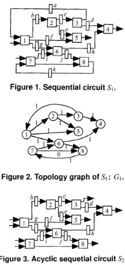
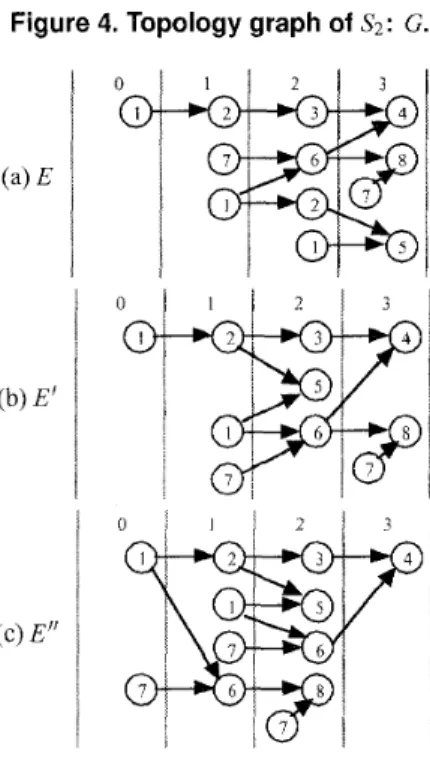
Z+ (Z+ denotes a set of non-negative integers), and r(u,v) represents the number of registers on a connection 0Example 1: Consider a sequential circuit SI illustrated in Fig. 1. In this figure, 1 , 2 , .
.
. , 8 are logic blocks and a , b, . . . , k are registers. The topology graph of this circuit SI is shown in Fig. 2.Definition 2 (Time expansion graph (TEG)): Let S be an acyclic sequential circuit and let G = (V,A, r ) be the topol-
0
U
Figure 1. Sequential circuit S,
.
Figure 2. Topology graph of SI : GI.
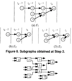
Figure 3 . Acyclic sequetial circuit 5’2.
ogy graph of S. Let E = (VE,AE,t, 1) be a directed graph, where V , is a set of vertices, A E is a set of arcs, t is a map- ping from VE to a set of integers, and 1 is a mapping from VE to the set of vertices V in G. If graph E satisfies the follow- ing four conditions, graph E is said to be a time expansion graph (TEG) of G.
Cl(Logic block preservation) The mapping 1 is a surjec- tive, i.e.,
v v E V,3U E VE s.t. v = I ( u ) .
CZ(1nput preservation) Let U be a vertex in E . For any direct predecessor v (E p r e ( Z ( u ) ) ) of U in G, there ex- ists a vertex U’ i n E such that l(u’) = v and U’ E pr.e(u). Here, pre(v) denotes the set of direct predecessors of C3(Time consistency) For any arc (u,v) (E A E ) , there exists an arc (I(u),l(v)) such that t ( v ) - t ( u ) = C4(Time uniqueness) For any vertices u,v ( E V E ) , if
t ( u ) = t ( v ) and if I ( u ) = l ( v ) , then the vertices U and v are identical, i.e., U = v.
V .
r(l(U),l(V))-
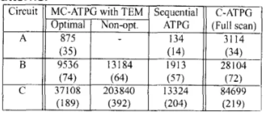
0 Example 2: Fig. 4 shows the topology graph G of an
Figure 4. Topology graph of S2: G.
l o 1 1 1 2 ~ 3 1
4
(cj E”
3
Figure 5. Example of TEMs of G.
acyclic sequential circuit S2 in Fig. 3. Fig. 5 shows TEGs of G. In Fig. 5 , the number denoted in a vertex U is the label of the corresponding one I ( u ) in G, and the number located at the top of each column denotes the value of the labels t ( u ) of the vertices u in the column. Each of graphs E,E’,E” satisfies all the conditions in Def. 2. U Note that as shown in the above example, the TEG of a topology graph is not unique in general.
Definition 3 (Time expansion model (TEM)): Let S be an acyclic sequential circuit, let G = ( V , A , r ) be the topology graph of S, and let E = ( V E , A E , ~ , ~ ) be a TEG of G. The combinational circuit CE ( S ) obtained by the following pro- cedure is said to be the time expansion model (TEM) o f S based on E .
For each vertex U E VE, let logic block Z(u) ( E V ) be the logic block corresponding to U.
For each arc ( U , v ) E A E , connect the output of u to the input of v with a bus in the same way as (I(u),l(v)) (E A ) . Note that the connection corresponding to ( u , v ) has no register even if the connection corresponding to
Figure 6. TEM of S2 based on E : c~(S2).
(l(u),l(v)) has a register (i.e., r(l(u),l(v)) > Oj. (3) For a line or a logic gate in each logic block obtained
by Steps (1) and (2j, if it is not reachable to any input of other logic blocks, then it is removed.
U
Example 3: Fig. 6 shows the TEM of a sequential circuit S2 (Fig. 3) based on TEG E (Fig. 5(a)). In this figure, a highlighted part in a logic block represents a portion of the lines and gates removed by Step (3) in Def. 3. U
2.2. Test Generation with TEM
Here we consider the relationship between inputioutput sequences of an acyclic sequential circuit and inputloutput patterns of its TEM. Let S be an acyclic sequenl.ia1 circuit, and let G = ( V , A , r ) be the topology graph of S. Let E = ( v ~ , A ~ , t , l ) be a TEG of G, let C E ( S ) be the TEM of S based on E , and let t,in be the minimum of labels t in CE ( S ) .
An input pattern for CE(S) can be transformed into an input sequence for circuit S by the following procedure T S .
Definition 4 (Transformation procedure ZS): For each logic block U E VE in C E ( S ) , let an input pattern I,, for ZL
be the input pattern Il(,) ( t ( U ) - tmin) which is applied to the 0
Lemma 1: Let IC be an arbitrary input pattern for TEM C, ( S ) , and let ~ ( l c ) be the input sequence obtained fromIc by procedure ZS for S. The output pattern 0, obtained from a logic block U E VE by applying input pattern IC to CE (S) is equal to the output pattern O,,,,,(t(u) - tmin) obtained from the corresponding logic block I ( U ) at time t ( U ) - tmin by ap- plying input sequence ~ ~ ( i c ) .
(Proof.) Let U’ (E p r e ( u ) ) be an arbitrary logic block con- nected to an input of logic block U. By condition C2, in
s,
the logic block Z(U’) corresponding to U’ is connected to the input of l ( u ) . By procedure ZS, an input pattern I,/ for U’is transformed into the input pattern I/(,,) ( t ( U ’ ) - tmin) for I(u’) at time t(u’) - tmin. From condition C4, we can say that the number of patterns to be applied to Z(u’) at time t ( u ’ ) - tmin is just one. The effect of applying I,(,/) (t(u’) -
tmin) reaches l ( u ) r(l(u’),l(u)) clocks later. Here, note that r ( Z ( d ) , l ( u ) ) denotes the number of registers between logic blocks Z(U’) and I ( u ) . From condition C3, we can say that corresponding logic block Z ( U ) at time t ( u ) - tmin.
(a) Input and output patterns for C E ( S ~ ) .
(LB: Logic block)
(b) Input and output sequences transformed for S2 Figure 7. Trainsformation procedure SS.
(t(u’) -t,,in) + r ( I ( u ’ ) , Z ( u ) ) = t ( u ) -tmjn. Thus, the lemma
is proved. 0
Example 4: Consider a TEM c~(S2) (Fig. 6) of a se- quential circuit S2 shown in Fig. 3. Suppose that as shown in Fig. 7(a), an input-pattern Zc = (Zl,Zi,Z:,Zz,Zl) is ap- plied to c ~ ( S 2 ) and the corresponding output-pattern is OC = (03,O4,O5, Os). According to the labels t in TEG E (Fig. 5(a)), the patterns IC and OC are transformed into the sequences shown in Fig. 7(b) by procedure SS. Here,, X
denotes a don’t-care value. 0
Note that the length of the sequence obtained from a pattern for TEM C E ( S ) by procedure 7s becomes Let I . be an input sequence for acyclic sequential circuit S such that the sequence determines the output pattern O.,(t) of a logic block v (E V ) in S at time t . Here, a pattern 1:hat does not affect O,(t) im the input sequence Is is considered as don’t-care. Input sequence Is for S can be transformed by the following procedure.
Definition 5 (Transformation procedure zc): ( I ) Select a logic block U (E I-’ (v)) from the set of logic blocks I-’(.) corresponding to v. (2) For every input pattern I d ( t ’ ) ap- plied to each logic block v’ at time t’, if Id (t’) affects output O,(t), then let I d ( t ’ ) be the input pattern Z,!for the logic block that satisfies U’ E I-’ (v’) and t(u‘) = t ( u ) - ( t - t’). maxuEvE{t(u)) -millut:v,{t(u)}
+
1.m U
Lemma 2: Let v (E V ) be an arbitrary logic block in acy1:lic sequential circuit S, and let Is be an input sequence that is required to set the output of v to O,(t) at time t. The output
pattern 0, obtained from the logic block U corresponding to v by applying the input pattern ~ ~ ( 1 s ) is equal to output pattern 0, ( t ) .
(Proof.) From condition C 1, we can say that there exists at least one vertex RI (E I-’ (v)) that corresponding to vertex v. Let v’ (E p r e ( v ) ) be any logic block connected to the input of logic block v. By condition C2, the logic block U ’ ( € I-’(v’)) conresponding to v’ is connected to the in- put of U . The input pattern that is applied to v’ and that affects the outpul pattern O,(t) of v at time t is the pat- tern Z,t(t - r(v’,v)) which is applied at time t - Y(v’,v).
Here, note that Y(v’,v) is the number of registers between logic blocks v’ anld v. Input pattern 1,s (t - r(v’,v)) is trans- formed into the input pattern for U’ such that t(u’) = t ( u ) - (t - (t - Y(v’,v))) = t ( u ) - r(v’,v). From conditions C3 and C4, we can say that the number of patterns that sat- isfy t ( u ’ ) = t ( u ) -- r(v’,v) is just one. Thus, the lemma is
Next, let us consider the relationship between faults in an acyclic sequential circuit and those in its TEM. Here we consider single stuck-at faults in logic blocks as those in an original sequential circuit. The stuck-at faults on lines between logic blocks and in registers can be considered to be equivalent to those on inputioutput lines of logic blocks. Definition 6 (Fault in TEM): Let S be an acyclic sequen- tial circuit. Let G = (V,A, Y ) be the topology graph of S, let E = (VE,AE,~,Z) be a TEG of G, and let C E ( S ) be the TEM of S based on E . L,et F be the set of faults in S, and let FE be the set of faults in C E ( S ) . Suppose a fault ,f E F in a logic block U in circuit S. Let fe E FE be the fault correspond- ing to fault f . Fault fe is a multiple fault that consists of all the faults that exist on the same line in every logic block
U E I-’(.). That is, if the number of logic blocks U such that I ( u ) = v is just one, then the fault .fe is a single fault, 0
proved. 0
otherwise, ,fc is a multiple fault.
Theorem 1: Let S be an acyclic sequential circuit. Let G = ( V , A , r ) bethetopologygraphofS, letE = ( v ~ , A ~ , t , l ) be a TEG of G, artd let CE ( S ) be the TEM of S based on E . Let F be the set of faults in S, and let FE be the set of faults inCE(S). Then,
(1) There exists a test sequence for a fault f E F if and only if there exists a test pattern for the fault
fe
E FE corresponding to fault f .(2) A test pattern for a fault f e E FE can be transformed into a test sequence for the fault f E F corresponding to fault f e .
(Proof.) Let Tf be a test sequence for fault f . Let tfr be a test pattern for fault f e . Let Sf be a faulty circuit with f of S. Let C E ~ ; , ( S ) a faulty circuit with fe of C E ( S ) . Fault
fe
is a multiple fault that consists faults in every logic block lP’(v) corresponding to the logic block v (E V ) in which exists fault f . Heme, the structure of C E ~ , ; ( S ) is the same as
that of the TEM CE (Sf) of Sf based on TEG E . Therefore, by Lemma 2, test sequence Tf obtained by procedure T~ can detect fault f c . Further, by Lemma I , test pattern t f obtained by procedure 7,s can detect fault f. Thus, the theorem is
proved. 0
3. RT Level Partial Scan Design
As mentioned in the previous section, an acyclic sequen- tial circuit can be tested with its TEM by using a combina- tional test generation algorithm (provided that it is capable of multiple stuck-at faults). Test generation with TEMs can be applied to general sequential circuits by cutting all the loops with scan FFs prior to the test generation. The feed- back loops to be cut can be determined at the RT level (or before logic synthesis) since the cut loops depend only on the circuit structure
’.
The RT level scan design method is as follows.(Pl) Scan register selection. Determine a set of scan reg- isters that make a given RT level circuit S’ acyclic. It can be done with the minimum hardware overhead (or the minimum number of scan registers) by applying the minimum feedback vertex set (MFVS) algorithm [3,4]. Let SgFT be a scan-designed circuit S R , and let S: be an acyclic kernel o ~ S ~ F T .
(P2) TEM construction. Construct the topology graph G of S,“. The topology graph of an RT level circuit can be obtained by substituting ‘a functional module’ such as adders for ‘a logic gate’ in Def. 1. Create a TEG E of G. Construct the TEM of S: based on E .
(P3) Logic synthesis. Obtain a gate level circuit S D F ~ cor- responding to the scan-designed RT level circuit SgFT by logic synthesis. Further, obtain a gate level circuit C E ( S ~ ) corresponding to acyclic kernel C E ( S ~ ) . (P4) Test generation. Define the fault list F for acyclic
kernel Sa. Based on Def. 6, define the fault list FE for CE(&), corresponding to F . Generate a test set T, for FE with a combinational test generator capable of dealing with multiple faults.
(P5) Test sequence transformation. Transform test set
TL
into a test sequence Ta for acyclic kernel Sa by pro- cedure zs. Finally, transform Tu into a test sequence Ts applicable to SDFT via scan.Note that in the second procedure (P2), the time required to obtain a gate level TEM C E ( & ) is small because all the combinational modules in the TEM are the same as those in its original RTL circuit.
3.1. Testing Cost Minimization Problem
In general, the number of TEMs for an acyclic sequential circuit is more than one. The difference of TEMs is consid-
’Provided that memory elements such as flip-flops are neither removed nor retimed during logic synthesis.
ered to affect its test generation time and the generated test sequence. Hence, the TEM constructed at Step (2) in the above-mentioned procedure is important to reduce the cost of testing. The relationship between a TEM and the testing cost can be considered as follows.
(1) TEM size. As the size of a TEM increases, the test gen- eration time for it also increases.
(2) Multiple faults. Recall that there exist multiple faults in a TEM. The number of multiple faults and the num- ber of faults that compose a multiple fault affects the cost of test generation.
(3) Number of PPIOs. In a TEM, the primary inputs and outputs corresponding to scan registers are referred to as pseudo-primary inputs and outputs (PPlOs). Pat- terns for PPIOs are transformed into scan sequences. Note that an inputioutput pattern for a logic block U
whose label is t ( u ) are transformed into those at time
t ( u ) . Hence, as the number of labels t that are affixed to logic blocks having PPIOs increases, the test appli- cation time also increases.
Example 5: A sequential circuit SI in Fig. I becomes acyclic by replacing registers U and k with scan registers. Suppose that its acyclic kernel and the topology graph are S2 and G shown in Figs. 3 and 4, respectively. Note that the vertices labeled by 1,3,7 and 8 represent logic blocks which have PPIOs. Then, consider three TEGs E , E‘ and E” of G illustrated in Fig. 5 . The total number of vertices, the maximum number of faults composing a multiple fault and the number of vertices having PPIOs of E , E’ and E” are (12,3,4),( 10,2,4) and (12,3,3), respectively. 0
Here, let us consider the first problem (1) 3.2. Problem Formulation
Let G = ( V , A , r ) be the topology graph of an acyclic sequential circuit Sa. Let E = ( v ~ , A ~ , t , l ) be a TEG of G, and let C E ( S ~ ) be the TEM of S, based an E . Let w(v) (w : V
+
Z+) be the number of gates in logic block v E V (or the estimate of the logic size for an RT level mod- ule v). The logic size of TEM CE(&), ~ ( C E ( & ) ) , is ex- pressed asf(CE(Su)) =
c
w(l(u)).U F r’,
Then, the following problem is formulated using the above equation.
Minimum TEM Problem
Given: The topology graph G = ( V , E , r ) of an acyclic se- quential circuit Sa, the number w(.) of gates in each logic block v E V .
Solution: An optimal TEM Eopt which minimizes function
f
(CE ( s a ) ).3.2.1. Algorithm and Complexity
Recall that for a topology graph G, multiple TEGs E can be derived. For any vertex v in E , a subgraph such that ver- tex v is a sink vertex (i.e., its outdegree is zero) is, howcver, uniquely determined by conditions C2, C3 and C4. Accord- ingly, an algorithm for constructing a TEG E is as follows. Algorithm: Construct TEA4
1. Let Vi
(c
V ) be a set of vertices whose outdegree is 0 in topology graph G. For each vertex v E Vi, determine the corresponding vertex U E VE such that /(U) = v, and let U be the set of those vertices U.2. For each vertex U E U , define t(u) = t where t is an arbitrary integer, and construct a subgraph whose isink vertex is u under conditions C2, C3 and C4. Let 13 be the set of those graphs.
3. Let E :=
4.
4. (1) Select a subgraph Ej = (5, Ei, ti, li) E E .
(2) For each vertex v E 5, let ti(.) := retime(ti(v)), where retime() is a function that returns an integer {(de- scribe below).
(3) Merge E, with E under the condition C4, and sub- stitute the resultant graph for E .
(4) Let E : = E - { E j } . I f E
#
$, then go to 1. 5 . The resulting graph E becomes a TEG for G. At Step 4.(2), the function retime() modifies the label t ( ) of graph Ei, and accordingly the TEG E obtained by the above algorithm will change. Consequently, the size ~ ( C E ( & ) ) of TEG C E ( & ) will also change.For each subgraph, Ei = (F,Aj,tj,lj) E E, which is ob- tained at Step 2, let
dj = maxucK{ti(u)} -minutt;{ti(u)}.
The range of values calculated by function retime() is ex- pressed as D =
EL,
di where m = /El. Hence, the range of the label of each vertex in E, is expressed as s; = D - d, -t 1. Therefore, the total number of feasible solutions, i.e., the to- tal number of TEMs that can be calculated to find an optimal TEM is expressed as s; = O ( D m ) . in particular, when the length of the test sequence obtained by procedure zs is minimized, it is expressed as d,,, = max{di}, and hence, the number of TEMs that should be considered becomeso(d;ax).
3.2.2. Heuristic Algorithm
Here we present a heuristic algorithm for finding an op- timal TEG Eopt which minimizes function ~ ( C E ( & ) ) . In order to find an optimal solution efficiently, the order of se- lecting a subgraph E, at Step 4.( 1) and the value determined by function retime() at Step 4.(2) are important. Thus, the followings are substituted for Steps 4.(1) and 4.(2). Algorithm: ConstructMin TEA4
4.( 1 ’) Select a subgraph Ei such that di is the maximum.
(b) E2 ( 3 ) E3
Figure 8. Subgraphs obtained at Step 2.
Figure 9. TEM of S2 based on E’: CEf(S2).
4.(2’) Let function retime() return a value that minimizes function f(E) of graph E constructed at Step 4.(3). Example 6: Consider a topology graph G illustrated in Fig. 4. Here, we assume that b’v 6 V , W ( V ) = 1 for the sake of simplicity. Fig. 8 shows the subgraphs obtained at Step 2 in the algorithm. The order of subgraphs selected at Step 4.( 1 ’) becomes E l , E2, E3, and the resultant TEG becomes E’, whose function is expressed as f ( C p (S2)) = 10. shown in Fig. 5(b). This value 10 is the minimum, and hence E’ is optimal. Fig. 9 shows the corresponding TEM C p (S2).
4. Experimental Results
We made experiments on test generation with time ex- pansion models (TEMs) using several register-transfer level (RTL) data path circuits. Table 1 shows the characteristics of the data path circuits. In this table, the values in paren- theses present the characteristics of gate level implementa- tions obtained by Synopsys Design Compiler. The number of gates denoted by ’#gates’ was evaluated using two-input NAND gate equivalent.
On these experiments, we made the circuits acyclic with the minimum number of scan FFs (Table 2), derived opti- mal TEMs for the acyclic kernels by the proposed heuris- tic algorithm ConstructMinTEM, and generated test pat- terns for the optimal TEMs using a combinational ATPG capable of dealing with multiple stuck-at faults (denoted by MC-ATPG). In order to explore the effectiveness of test generation with the optimal TEMs, we also made experi-
Table 1. Circuit characteristics. Table 3. Characteristics of optimal and non-
#modules: Number of modules (e.g. adders, multipliers).
#PIS: Number of input ports.
#POX Number of output ports.
#regs: Number of registers.
Table 4. Experimental results. CPU time [sec.] Table 2. Partial scan for cycle-breaking.
Circuit
11
#scan-regsI
#scan-FFsI
depth1
#terminals1 I R I 3 1 1
#scan-regs: Number of scan registers.
#scan-FFs: Number of scan flip-flops. depth: sequential depth, i.e., maximum number of
FFs on any path in the circuit.
#terminals: Number of modules that has no output connected to other modules (i.e., #terminals corresponds to the node whose outdegree is zero in the topology graph)
ments on test generation with non-optimal TEMs and those on test generation using a sequential ATPG without TEMs. Non-optimal TEMs were calculated so that the TEM size became large. Moreover, assuming full scan, we generated test patterns for the combinational parts of the circuits using a combinational ATPG capable of dealing with only single stuck-at faults (denoted by C-ATPG). All experiments were performed on a SUN workstation SS20.
Table 3 shows the characteristics of optimal and non- optimal TEMs. For all the circuits, it was confirmed that the optimal TEM was calculated by ConstructMinTEM in less than one CPU second. Note that the TEM for the ker- nel of circuit A is determined uniquely since it has just one module that has no output connected to other modules (col- umn #terminals in Table 2), and accordingly the number of subgraphs constructed in the algorithm Construct T E M is just one. For circuits B and C, it was confirmed that the size (i.e., the number of gates) of the TEM obtained by ConstructMinTEM is the minimum.
As a test generator, Matsushita Mint [ 171 was used. Mint has two modes for single stuck-at faults; combinational test generation and sequential one. The MC-ATPG was imple- mented by modifying the combinational ATPG package in Mint.
Table 4 and 5 report the CPU time required by ATPG algorithms and the fault efficiency, respectively. From these tables we can see that the CPU time required by MC-ATPG for the optimal TEM is smaller than that for the non-optimal TEM for both circuits B and C. Moreover, for circuits B and
required by ATPG.
674 88 1 1882 109
1758
Table 5. Experimental results. Fault efficiency [“h]
.
Circuit MC-ATPG with TEM Sequential C-ATPG
94.42 100.00
99.87 99.85 98.26 100.00
99.76 99.01 99.52 99.89
C, we can see that the time required by MC-ATPG with the optimal TEM is smaller than that by sequential ATPG while the fault efficiency obtained by the MC-ATPG with optimal TEM is larger than that by sequential ATPG. Although the CPU time required by MC-ATPG with the optimal TEM is larger than that by C-ATPG for full scan for circuit A, the fault efficiency obtained by MC-ATPG using its optimal TEM is larger than that obtained by sequential ATPG and it is almost complete (100%).
Table 6 shows the number of test patterns to be applied to scan-designed circuits provided that the scan design is implemented with one scan chain. In this table, the number in parentheses denotes the number of test patterns generated by ATPGs (not including patterns required by scan). From this table we can see that the number of test patterns gener- ated by test generation with optimal TEMs is smaller than that for full scan circuits for all the circuits. This is because the number of scan FFs in the acyclic partial scan design is smaller than that in the full scan design (Table 2), and thus the number of test patterns required for scan operation becomes smaller.
As a result, from these experiments, we can see that our partial scan and test generation approach is effective in re- duction of hardware overhead and test length compared to full scan approach.
Table 6. Experimental results. Number of test patterns.
5.
ConclusionsWe introduced time expansion models (TEMsi for acyclic sequential circuits and proposed a register-transfer level partial scan design method based on the approach. We proved that an acyclic sequential circuit can be test- generated with its TEM using a combinational ATPG capa- ble of dealing with multiple faults, and proposed a hearis- tic algorithm for finding an optimal TEM which minirnizes the test generation time. Experimental results show that the proposed algorithm can find optimal TEMs efficiently and that test generation using optimal TEMs is effective in reduction of hardware overhead and test application time compared with full scan approach while the fault efficiency is almost complete.
In this paper, we formulated a TEM optimization prob- lem provided that the test generation time increases as the size of a TEM increases. However, test generation time for TEMs may correlate with other factors such as ntulti- ple faults and the logic level. We will further investigate the characteristics of TEMs with respect to the test generation time. To consider an optimal TEM which minimizes the test length is a remaining problem.
Acknowledgments
The authors would like to thank Mr. Michiaki Murhoka, Mr. Shiro Tsuji, Mr. Mitsuyasu Ohta and Mr. Toshihiro Hi- raoka of Matsushita Electric Industrial Co., Ltd., Japan, and Prof. Toshimitsu Masuzawa and Prof. Michiko h o u e of Nara Institute of Science and Technology, Japan for their fruitful comments and discussions.
References
H. Fujiwara, Logic Testing and Design for Testability, The MIT Press, 1985.
M. Abramovici, M.A. Breuer, and A.D. Friedman, Digi- tal Systems Testing and Testable Design, Computer Sc ence Press, 1990.
K.-T. Cheng and V.D. Agrawal, “A partial scan method for sequential circuits with feedback,” IEEE Trans. Cowput., Vo1.39, No.4, pp.544548, Apr. 1990.
[4] D.H. Lee and S.M. Reddy, “On determining scan flip-flops in partial-scan design approach,” in Proc. Int. Conf Computer- Aided Design, pp.322-325, Nov. 1990.
[5] R. Gupta, R. Gupta, and M.A. Breuer, “The BALLAST methodology for structured partial scan design,” IEEE Pans. Comput., Vo1.39, No.4, pp.53&544, Apr. 1990.
A. Balakrishnan and S.T. Chakradhar, “Sequential circuits with combinational test generation complexity,” in Proc. Int. Conf on VLSI Design, Jan. 1996, pp, 1 1 1-1 1 7,
T. Takasaki, T. Inoue, and H. Fujiwara, “Partial scan de- sign methods based on internally balanced structure,” in Proc. Asia & South Pacific Design Automation Con$, 1998, V. Chickermane, J. Lee, and J.H. Patel, “Design for testa- bility using architectural descriptions,” Proc. IEEE Int. Test Con$, pp.752-761, 1992.
T.-C. Lee, N.K. Jha, and W.H. Wolf, “Behavioral synthesis of highly testable data paths under the non-scan and partial scan environirnents,” in Proc. ACM/IEEE Design Automation Con$, 1993, pp.292-297.
S. Dey and M. Potkonjak, “Non-scan design for testability of RT-level data paths,” in Pvoc. Int. Conf Computer-Aided Design, 19941, pp.640-645.
A. Motohara, S. Takeoka, T. Hosokawa, M. Ohta, Y. Takai, M. Matsumoto, and M. Muraoka, “Design for testability us- ing register-transfer level partial scan design,” in Proc. Asia
& South Pacijic Design Automation Cor$ , 1995, pp.209- 215.
K. Takabatake, M. Inoue, T. Masuzawa, and H. Fujiwara,
“Non-scan design for testable data paths using thru oper- ation,” in Proc. Asia & South PaciJc Design Automation Con$, 1997, pp.3 13-3 18.
T. Hosokawa, K. Kawaguchi, M. Ohta, and M. Muraoka,
“A design for testability method using RTL partitioning,” in Proc. IEEE Asian Test S’mp., 1996, pp.88-93.
R. Gupta ancl M.A. Breuer, “Partial scan design of register- transfer level circuits,” Journal of Electronic Testing: Theoiy and Applications, V01.1, pp.25-46, 1995.
A. Kunzmann and H.-J. Wunderlich, “An analytical ap- proach to the partial scan problem,” Journal of Electronic Testing: Theor?/ and Applications, Vol. I , pp. 163- 174, 1990. R. Gupta and M.A. Breuer, “Testability properties of acyclic structures and applications to partial scan design,” in Pvoc. IEEE VLSI Test Symp., 1992, pp.4%54.
A. Motohara, T. Hosokawa, M. Muraoka, H. Maekawa, K. Kayashima, Y. Shimeki, and S. Shin, “A State Traver- sal Algorithm Using a State Covariance Matrix,” in Proc. ACM/lEEE L)esign Automation Con$, 1993, pp.97-10 1. pp.211-216.