Scan Cells Reordering to Minimize Peak Power during
Scan Testing of SoC
Jaynarayan T Tudu∗, Erik Larsson†, Virendra Singh∗, and Hideo Fujiwara‡
∗ Indian Institute of Science, Bangalore, India, Email: jayttudu@csa.iisc.ernet.in, viren@serc.iisc.ernet.in
† Linkoping University, Linkoping, Sweden Email: erila@ida.liu.se
‡ Nara Institute of Science and Technology, Nara, Japan Email: fujiwara@is.naist.jp
Abstract—1Scan circuit testing generally causes excessive switch- ing activities compared to normal circuit operation. Higher switching activities causes two problems 1. supply voltage droop and 2. chip damage if peak activities last for sufficient number of shift cycle. This paper proposes a methodology to minimize the peak power consumption during scan shift operation. The proposed methodology consists of a graph theoretic problem formulation and corresponding algorithm. The experimental results show that the proposed methodlogy is able to reduce upto 49% of peak power compared to the solution provided by industrial tool.
Index Terms—Peak Power, Scan Circuit, Power Droop, Scan Cells Ordering.
I. INTRODUCTION
In a scan circuit, a set of sequential elements are connected to each other in a serial fashion known as scan chain. The scan pattern required to set the state of the scan cells has to be loaded into the scan chain by shifting it in serial shift manner. During the time of serial shifting of scan patterns there are number of transitions occur in the scan chain. These transitions in turns creates many more toggles in the combinational part and hence the dynamic power consumption. The toggling activity that takes place during scan operation is generally double than the normal functional operation. This dynamic power dissipated during scan shift operation is generally studied in terms of average and peak power [14]. As most of the modern designs have characteristic of being: very complex, having small feature size and high speed, the power consumption becomes an important issue to address for the following reasons: excessive average power can cause the problem such as instant circuit damage, higher product cost, performance degradation and reduced battery life time in case of online testing [14] ; and excess peak power results into IR drop and cross talk problem due to which a good chip can falsely be classified as defective chip [2] [1].
To reduce average power during test mode, many solutions have been proposed such as reducing test clock frequency, circuit partitioning(circuit modification), test vector reordering, scan
1The research is partially supported by The Swedish Foundation for Interna- tional Cooperation in Research and Higher Education(STINT) by an Institutional Grant for Young Researchers.
chain reordering, scan masking and X-filling. Although most of the work on average power also able to reduce the peak power, there is not many work explicitly targetting peak power issue. However, due to the change in design characteristic, the peak power issue becomes increasingly important for scan testing. The peak power is big issue for at-speed testing. During high speed operation, the excessive peak power causes high rate of current in the power and ground rails and hence leads to excessive noise at power and ground. This excessive noise can change the state of logic unexpectedly hence this may cause some good die to fail the test which leads to yield loss [13]. The IR drop and cross talk problem due to peak power is discussed in detail in [2]. The peak power issue in test mode is generally studied in three different scan cycles, these are, peak power consumption during load/unload cycle, during shift
& launch cycle(also known as test cycle), and during capture cycle. The peak power during load/unload and capture cycle is important to minimize to avoid the problem of chip damage during testing [14]. The peak power during test cycle is important to reduce to avoid the problem due to IR drop and cross talk [13]. Reduction of peak power during test becomes necessary for three important reasons: 1. Higher peak power causes yield loss due to power droop and cross talk, 2. To avoid chip damage during testing, and 3. If the circuit is a module in an SoC then multiple module can be scheduled together to minimize test time.
In this paper we have address the problem of peak power during scan shift operation. The main contribution of this paper is to provide a scan cells reordering methodology that takes power consumption during all cycles(shift in, shift out and capture) into account.
The rest of the paper is organized as follows. Section II gives an overview of previous works. In Section III, a brief background to peak power problem and basic of scan reordering is presented. Section IV presents the problem formulation for scan cells reordering. Section V provides the proposed algorithm. In section VI, time and space complexity for the proposed algorithm is analyzed. Section VII presents the experimental results and the paper is concluded with conclusion in section VIII.
10th IEEE Workshop on RTL and High Level Testing (WRTLT'09), pp. 43-48, Nov. 2009.
II. PREVIOUSWORK
The problem of test power reduction has been an active area of research for quite sometime. The most straight forward approach to reduce the average power consumption is to do test at reduced speed. However this solution is no longer a practical as modern design are sensitive to test application time. More over the peak power is independent of clock frequency, hence peak power needs different account. Most of the solutions [11], [9], [4], [12] are aimed at average power reduction however they have also achieved some reduction in peak power as as a bi-product. Chou et al. [11] proposed the scheduling of test under power constraint. This work addresses the power issue at module level, essentially not at circuit level. The work by Dabholkar et al. [9] has achieved average power reduction by test vector as well as by scan latch reordering by using some of the TSP heuristics. The primary concern of Dabholkar et al. is the average power. The work in the area of pattern compaction technique to control the average as well as peak power is done by Sankaralingam et al. [4]. The idea is to carefully merge the test patterns such that the power consumption in the resultant patterns is minimized. However, the scan reordering can still be applied on power aware merged patterns. Another work on average power reduction is done by Girarad et al. [12] and Bonhome et al. [10]. The basic idea behind these work is to reorder the scan chain. In both of these works, the problems are formulated as graph theoretic problems. As the problems are NP-complete the solutions are heuristic based. Furthermore the work by Girard [12] also provides the power - area tradeoff. Some of the work in the area of X-fill to reduce average power are presented by Butler et al. [5] and Li et al.[8]. The underlying principle behind X-fill is to reduce the number of transitions within pattern. The worth noting point in this kind of work is the proper balance in using the number of X’s for power reduction and for pattern compaction.
As discussed in the previous section, peak power reduction is becoming increasingly important. A few works have been pro- posed in peak power reduction [7], [3], [13], [6]. Sankaralingam et al [7] first identify the peak power violation patterns, and then a simulation is performed to identify the X’s in those patterns. These X’s are used for power reduction. This kind of methodology generally involves the process of simulation which may become time consuming for large circuits. In Badereddine et al. [3] work an experiment is carried out to evaluate the peak power reduction using MT-fill. The work done by Corno et al. [6] is also address the peak power problem. In this work X’bits are identified by process of simulation and specified for peak power reduction. A recent work reported by Tudu et al. [15] uses scan vector reordering to minimize peak power. However our approach of scan chain odering can still be applied along with their technique. Hence a further reduction can be achieved.
The work done by Badereddine et al. [13] is based on the scan reordering to minimize peak power during test cycle. In this work, the problem is formulated as a simulated annealing problem. Their objective was to reduce peak power during test cycle however they have also achieved some nominal reduction
in peak power during load/unload cycles as a bi-product. Based on the above observation, in this paper we are proposing a methodology to exploit the concept of scan cells reordering to minimize peak power during shift and test cycle of scan operation. The proposed methodology does not affect the fault coverage and test time however incur nominal area overhead due to cell routing.
III. BACKGROUND
A. Overview of Peak Power Issue
The power dissipated during shift operation is due to the three categories of transition 1. Intra pattern transition, 2. Inter pattern transition and 3. Combined intra pattern transition. Intra pattern transionis transition that arises due to the difference between any consecutive bits in a particular pattern(stimulus or response). Inter pattern transitionis caused by the transition between the last bit of the response and first bit of the test vector. Combined intra pat- tern transitionis the sum of intra pattern transition of vector and intra pattern transition of response. In more formal way the peak power can be expressed as Pp= M ax∀i(#transition(V [i, 1]) +
#transition(R[l, i]) + #transition(V [1], R[l])), where i is the ith shift cycle, l is the length of scan chain, V[i, 1] is partially shifted in vector, R[l, i] remaining response bits to be shifted out. In this expression the first two factors contribute to intra pattern transition and combined intra pattern transition and the last factor contributes to inter pattern transition. Intra pattern transition can be minimized by minimizing internal transition in the vector and response. Combined intra pattern transition and inter pattern transition can be minimized by suitable combination of vector and response.
We addressed the intra pattern transition in this proposed methodology of scan cells reordering.
B. Basis of Power Reduction by Scan Cells Reordering
The scan chain reordering mechanism used for peak and average power minimization is basically relying on the reduction of intra pattern transitions. By looking at the differing bits in the pattern, each scan cell can be repositioned in a suitable order to reduce the intra pattern transitions. The reordering of scan cell will brings all 1’s close to each other and all 0’s close to each other while performing the scan shift operation. Because of the inherent limitation scan chain reordering cannot minimize inter pattern transition and combined intra pattern transition. Figure 1 demonstrates the basic principle to reduce intra pattern transition.
Initial ordering of scan chain Reordered scan chain SF0 SF1 SF2 SF3 SF4 SF5 SF0 SF2 SF5 SF1 SF3 SF4
1 ) 0 ) 1 ) 0 ) 0 ) 1 . 1 ) 1 ) 1 ) 0 ) 0 ) 0
Fig. 1. Basic principle of scan reordering
IV. PROBLEMFORMULATION
In this section a graph theoretic problem is formulated by first constructing a graph from given scan related information and then on that graph a problem resembling to scan cells ordering is defined. The following subsections explains the process of formulating the graph problem.
A. Construction of Graph
The important information that are needed to be reflected in the graph are, scan cells and peak power information for any pair of consecutive scan cells. Below is the procedure for graph construction:-
• For every scan cell SFi there is a corresponding node Ni in the graph.
• The connecting line between any two possible scan cells is represented by an undirected edge between respective nodes. Note:The edges are undirected because, the pairing of scan cells is symmetric with respect to the number of transition. For example, in Figure 1 a revers ordering of the reordered scan chain will also results into one transition.
• The instantaneous power consumed by any test vector or response due to any possible pair of scan cells is represented as a weight of the edge between respective nodes of the scan cells. The weight of edge in our formulation is a vector quantity, we name this weight as vector-weight. The vector- weightis computed as follows:
Computation of vector-weight: Each vector-weight keeps the instantaneous power information for all test stimulus and responses. Instantaneous power information for an individual pat- tern(stimuli or response) is computed by finding the bit difference between the original position of scan cell pair.
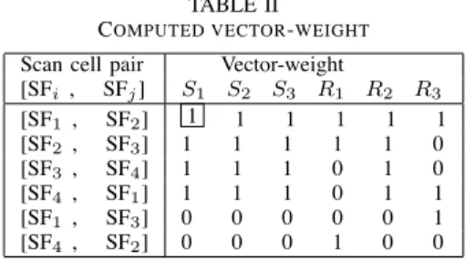
Table II shows the vector-weights for the scan pattern set(stimulus and responses) in Table I. The rows in Table I are test stimulus Siand corresponding test response Riand columns are scan flip flops SFi. In Table II the scan cell pairs are given in column labeled with “scan cell pairs” and corresponding vector- weightare given in the right hand side major column. The minor columns in the right hand side major column are the peak power information for each test stimuli Si and response Ri patterns. The rectangular box in Table I shows the bit difference due to scan pair SF1 and SF2 and the corrresponding instantaneous power information in Table II is kept inside a square box in S1 minor column. Figure 2 shows the complete vector-weighted graph constructed from the data given in Table I & Table II.
TABLE I
SCAN PATTERNS ANDORIGINAL SCAN ORDER
−→SF1−→SF2−→SF3−→SF4−→
S1 1 0 1 0
S2 0 1 0 1
S3 1 0 1 0
R1 1 0 1 1
R2 0 1 0 1
R3 1 0 0 0
TABLE II COMPUTED VECTOR-WEIGHT Scan cell pair Vector-weight
[SFi, SFj] S1 S2 S3 R1 R2 R3
[SF1 , SF2] 1 1 1 1 1 1
[SF2 , SF3] 1 1 1 1 1 0
[SF3 , SF4] 1 1 1 0 1 0
[SF4 , SF1] 1 1 1 0 1 1
[SF1 , SF3] 0 0 0 0 0 1
[SF4 , SF2] 0 0 0 1 0 0
In the process of computation of vector-weight, we have considered both test stimulus and responses. Taking both stimulus and response into account is sufficient to capture the peak power information that may either occur due to any of the stimulus or the responses.
B. Graph Theoretic Problem Formulation
This section will explain the principle of formulating the graph problem. The basic objective is that the formulation should consider the ordering of scan cells and the minimization of peak power.
The instantaneous power consumed by test patterns during scan shift operation due to scan cell pair [SFi, SFj] is represented as the vector-weight of the edge(Ni, Nj) in the graph. As the graph is a complete graph, it is always possible to find any order of scan cells by making a Hamiltonian path(which visits each node of the graph). Each possible Hamiltonian path in the graph has a corresponding cost cost(Ns, Ne)of constructing the path Ns− ⇠ −Ne, where Ns and Ne are start and end node in path. The cost of Hamiltonian path is determined differently for different types of problem. The computation of cost in our case is done by, first summing up all the vector-weights of each edge along the path, in vector addition manner. By summing up in vector addition manner the instantaneous power consumed by each individual test stimuli or response is preserved in the final summation result. Now in the final summation result the maximum instantaneous power among them will be the cost(Ns, Ne) for path Ns− ⇠ −Ne which resembles the peak power value for corresponding scan order Ss− ⇠ −Se. In a more formal way, cost can be expressed as cost(Ns, Ne)
= M ax 0
@ X
i,j✏(1,n)
vector-weight(Ni, Nj) 1
A, where Ni, Nj are adjacent nodes in path Ns− ⇠ −Ne,(1, n) is set of integer from
N1 [111111]
[111011]
[000001]
JJ JJ JJ JJ JJ JJ JJ JJ JJ JJ
J N2
N4
[000100]
tt tt tt tt tt tt tt tt tt tt
t [111010]
N3
[111110]
Fig. 2. A complete vector-weighted graph.
1 to n , and n is length of scan chain. The following example illustrates the above described procedure.
Example 1 Let N1[111011]N4[000001]N2[111110]N3be a Hamilto- nian path from Fig. 3. The vector summation of the vector-weight for this path = vector-weight(N1, N4) + vector-weight(N4, N2) + vector-weight(N2,N3)
= [1 1 1 0 1 1] + [0 0 0 0 0 1] + [1 1 1 1 1 0]
= [2 2 2 2 2 2]
The cost(N1, N3) = M ax[2 2 2 2 2 2] = 2, which is the peak power value for corresponding scan chain order.
Hence from above illustration the graph theoretic problem can formally be stated in following way:
Problem Statement: Given an undirected graph G(V, E, W), find a Hamiltonian path which has minimum cost over all other possible paths. Where V is set of vetices Vis, E is set of edges, and W is set of vector-weight.
Note: The hardness of problem is NP-complete as this can be reduced to TSP problem which is a known NP-complete problem.
V. PROPOSEDALGORITHM
As the problem is NP-complete we are proposing a greedy based polynomial time (with respect to V) algorithm. Our al- gorithm is different from any other greedy based heuristics in the way its determine the cost of making Hamiltonian tour.The complete algorithm has two subpart, Part-1 to find the Hamilto- nian cycle and Part-2 to find the path from Hamiltonian cycle. Following subsequent subsection gives the details of algorithm for Part-1 and Part-2.
A. Construction of Hamiltonian cycle
Problem Statement: Given a graph G(V, E, W) find a Hamiltonian cycle having minimum cost cost(Ns, Ne), here s= e.
The following steps explain the principle of the algorithm. Step 1: Chose an initial node as N1 and assign it to current- nodeand corresponding cumulative-node-cost as [0 0 0 0 0 0]. Note: cumulative-node-costis an array of integer values computed dynamically for a node visited currently.
Step 2: In this step, the decision parameter peak-power and average-power are computed. These are used in step 3 to select the next node to visit. The peak-power and average-power are computed with respect to the set of nodes which are not yet visited and are neighbors of the current node. We call these node as candidate-node and any edge from current node to a candidate- node is called as candidate-edge. A vector addition operation is performed between the cumulative-node-cost and vector-weight of each candidate-edge separately. We call these sum probe-path- weight. The peak-power for each of the candidate-edge is com- puted by finding M ax(probe-path-weight along the candidate-
edge). And average-power is computed by finding Sum(probe- path-weight along the candidate-edge).
Step 3: A node Ni from the set of candidate-node is selected as the next node if the peak-power along the edge(current-node, Ni) is minimum among all other peak-power. If there are more than one node having equal peak-power then the corresponding average-poweris used as a tie breaker. Following example helps understanding the above explanation.
Example 2 Considering Figure 2, the initial node will be N1
with cumulative-node-cost [0 0 0 0 0 0]. The neighboring node of N1 are N2, N3, and N4 which satisfies the property of being candidate-node because these are not yet visited. Based on the peak-power and average-power, a next node will be selected from these candidate-nodes. The corresponding candidate-edges are edge(N1, N2), edge(N1,N3), and edge(N1,N4). The vector- weight of each of these candidate-edge are [1 1 1 1 1 1], [0 0 0 0 0 1], and [1 1 1 0 1 1] respectively. Probe-path-weight along each of the candidate-edges will be vector addition of cumulative-node-cost of current node with the vector-weight of each of these candidate-edge which are,
[0 0 0 0 0 0] + [1 1 1 1 1 1] = [1 1 1 1 1 1], [0 0 0 0 0 0] + [0 0 0 0 0 1] = [0 0 0 0 0 1], and [0 0 0 0 0 0] + [1 1 1 0 1 1] = [1 1 1 0 1 1] respectively.
The peak-power and average-power along each candidate- edgecan now be computed as follows,
peak-power:
along edge(N1, N2,) = M ax([1 1 1 1 1 1]) = 1, along edge(N1, N3,) = M ax([0 0 0 0 0 1]) = 1, and along edge(N1, N4,) = M ax([1 1 1 0 1 1]) = 1. average-power:
along edge(N1, N2,) = Sum([1 1 1 1 1 1]) = 6, along edge(N1, N3,) = Sum([0 0 0 0 0 1]) = 1, and along edge(N1, N4,) = Sum([1 1 1 0 1 1]) = 5.
The next task is to select a next node based on the above computed peak-power and average-power. In this example peak- power along each candidate edge is equal i.e. 1, hence average- poweris used as a tie breaker. average-power along edge(N1, N3,) is 1 which is less than the average-power of other candidate edge. Hence node N3 will be selected as the next node to be visited.
Step 4: In this step cumulative-node-cost and current-node are updated. The cumulative-node-cost for next node to visit
= cumulative-node-cost of current-node + vector-weight of edge(current-node, next-node-to-visit). For Example 2, current- nodewill be updated with node N3and cumulative-node-cost for N3 = [0 0 0 0 0 0] + [0 0 0 0 0 1] = [0 0 0 0 0 1].
Step 5: Repeat the algorithm from Step 2 until a Hamiltonian cycle is construction.
At the end of this part, the algorithm will produce an inter- mediate result (Hamiltonian cycle). For the graph in Figure 2 algorithm Part-1 will give the Hamiltonian cycle shown in Figure
3 as output. N1
[000001]
SS SS SS SS SS SS SS SS
SS [111111] N2 [000100] N4
N3
[111010]
kk kk kk kk kk kk kk kk kk
Fig. 3. Hamiltonian cycle from Part-1 of algorithm
B. Construction of Hamiltonian path
Problem Statement: Given a Hamiltonian cycle H(V, E,W), find out a Hamiltonian path which have minimum cost cost(Ns,Ne). The problem can also be stated as, remove an edge from H having maximum power contribution in peak power.
Following step explain the process of removing a desired edge from given Hamiltonian cycle.
Step 1: First, all the vector-weight of edges will be summed up in vector addition manner. Then each vector-weight will be subtracted from the total summation result. Now from each subtraction result corresponding peak and average power will be computed(we call these computed peak and average power as remainder-peak and remainder-average power). Next step explains the use of remainder-peak and remainder-average power to select an edge to be removed.
Step 2: First, the edge to be removed will be searched based on the remainder-peak power. Any edge having minimum remainder- peakpower value will be the desired edge to be removed. In the case more than one edge having equal remainder-peak power value then their corresponding remainder-average power value will be considered to break the tie. It means the edge whose remainder-average power value is minimum will be the desired edge to be removed.
Example 3 illustrates the above steps.
Example 3 In this example Figure 3 will be used as a reference. Summation of all the vector-weights will be:
[0 0 0 1 0 0] + [1 1 1 0 1 0] + [0 0 0 0 0 1] + [1 1 1 1 1 1]
= [2 2 2 2 2 2]
Computation of remainder-peak power and remainder-average power corresponding to each edge is done as follows. For, edge(N1,N3) = [2 2 2 2 2 2] - [0 0 0 0 0 1] = [2 2 2 2 2 1] remainder-peak= M ax([2 2 2 2 2 1]) = 2
remainder-average= Sum([2 2 2 2 2 1]) = 11,
edge(N3,N4) = [2 2 2 2 2 2] - [1 1 1 0 1 1] = [1 1 1 2 1 2] remainder-peak= M ax([1 1 1 2 1 2]) = 2
remainder-average= Sum([1 1 1 2 1 2]) = 8,
edge(N2,N4) = [2 2 2 2 2 2] - [0 0 0 1 0 0] = [2 2 2 1 2 2] remainder-peak= M ax([2 2 2 1 2 2]) = 2
remainder-average= Sum([2 2 2 1 2 2]) = 11
edge(N2,N1) = [2 2 2 2 2 2] - [1 1 1 1 1 1] = [1 1 1 1 1 1] remainder-peak= M ax([1 1 1 1 1 1]) = 1
remainder-average= Sum([1 1 1 1 1 1]) = 6
From the above computation it can be observed that the removal of edge(N2,N1) is resulting into consumption of peak power = 1 which is minimum among all the edges and average power
= 6. Hence the removal of edge(N2,N1) will lead to a path having minimum cost. The corresponding minimum peak power consuming scan path will be SF1−!SF3−!SF4−!SF2.
VI. TIME ANDSPACECOMPLEXITY
In this section we analyze time and space complexity for proposed algorithm.
A. Time Complexity
Time to construct a Hamiltonian cycle: The proposed heuris- tic has complexity of %(n ⇤ l2) where l is the length of scan chain and n is number of test vector. The proposed heuristic takes additional 2n time to compute peak and average power at step 2 in part 1 of algorithm in comparison to any other heuristic of same nature whose edge weight in graph are just a scalar quantity unlike in our case.
Time to construct a Hamiltonian path: Time complexity for this part of algorithm is %(n ⇤ l).
B. Space Complexity
Space complexity to represent the graph is %(l⇤l). To store the cumulative-node-costrequires Θ(n). A temporary space to keep vector-weightis Θ(n). Hence overall complexity is %(l2+ n). Note:We donot use any explicit space to keep vector-weight for every edge in graph her we compute them on the fly from the test pattern file.
Hence the proposed heuristic does not suffer from any strain related to time and space.
VII. EXPERIMENTALRESULTS
The experiments are carried out on ITC99 and ISCAS89 circuits. The algorithm is implemented in C++. Scan insertion and circuit synthesis is done using industrial tool. Test patterns are generated using industrial tool. Test patterns are low power adjacent X’filled and compacted with low merge level of pattern compaction. Specification of benchmark circuits and experimental results are provided in Table III. For each benchmark circuit, Table III shows the number of transition for peak power due to industrial solution, due to [15], and due to proposed methodology and comparative results. The seventh column shows the % of reduction in peak power achieved by [15] and the last column shows the %of reduction achieved by proposed work. Experimental results show that the proposed work is able to reduce the power upto 49.67% for circuit b14. For the larger benchmark circuits like s9234, s13207, and s38417 proposed
TABLE III
CIRCUIT SPECIFICATION ANDEXPERIMENTAL RESULTS
Benchmark #test scan chain #gates #peak trans. #peak trans. %of reduct. by #peak trans. %of reduct. Circuit pattern length IndustrialSol by [15] [15]wrt indsol. ProposedSol. wrt indsol.
b04 50 66 597 33 32 3.04 24 27.27
b07 53 45 441 27 27 0 18 33.33
b08 40 21 183 16 15 6.25 11 31.25
b09 27 28 129 21 18 14.29 12 42.85
b14 625 215 5678 154 154 0 77 49.67
s420 53 16 218 11 9 0 9 18.18
s526 27 21 193 15 14 6.67 11 26.66
s1488 96 6 653 6 5 16.67 6 0
s5378 111 179 2779 84 83 1.20 75 10.71
s9234 128 211 5597 118 118 0 93 21.11
s13207 126 638 7951 335 334 0.30 253 24.47
s38417 129 1636 22179 627 624 0.48 528 17.38
algorithm is able to reduce 21% at an average. For benchmark circuit s1488 the proposed methodology unable to achieve any improvement. The reason is that the scan chain length for this circuit is very small where as the total test patterns are large in number. Also to see the effectiveness of the proposed algorithm we have compared our results with [15]. The table show that pro- posed algorithm is out performing the [15] for all the benchmark ciruits.
VIII. CONCLUSION
This paper has proposed a methodology to minimize peak power during scan shift operation. The results shows that pro- posed methodology is capable of minimizing peak power signif- icantly. The proposed methodology is a novel idea, as its open up a new way of formulating a graph theoretic problem for scan reordering. The proposed work keeps fault coverage and test time unaffected and also it does not incur any explicit area overhead. In our work we have not taken the routing area overhead in to account. However this problem of routing can also be solved by integrating our work with [12] where the proposed methodology can be applied within the cluster to take care of power and cluster ordering can be used to take care of routing congestion.
REFERENCES
[1] The International Technology Roadmap for Semiconductor, Design, 2007. [2] J. Saxena, K. M. Butler, V. B. Jayaram, S. Kundu, N. V. Arvind, P Sreeprakash
and M. Hachinger, “ A case study of IR-drop in structured in at-speed testing,” Proc. IEEE Int. Test Conf.,pp 1098-1104, Sept. 2003.
[3] N. Badereddine, P. Girard, S. Pravossoudovitch, C. Landrault, A. Virazel and H.-J. Wundelich, “Minimizing Peak Power Consumption during Scan Testing:Test Pattern Modification with X Filling Heuristics”, Proc. of Int’l Conf. on design and Test of Integrated System in Nano technology, pp. 359 - 364,2006.
[4] R. Sankaralingam, R. R. Oruganti and N. A Touba, “Static Compaction Technique to Control Scan Vector Power Dissipation” Proc. of VLSI Test Symposium,pp. 35-40, 2000.
[5] K.M. Butler, J. Saxena, T. Frayer, G. Herthenigton, A. Jain and J Lewis,“Minimizing Power Consumption in Scan Testing: Pattern Generation and DFT Techniques,” IEEE Int’l Test Conf., pp.335-364.
[6] F. Corno, M.Rebaudengo,M. Reorda, M. Violante, On Reducing the Peak Power Consumption of Test Sequences, European Conf. on Circuit Theory and Design,pp. 247-250, 1999.
[7] R. Sankaralingam et al., ”Controlling Peak Power during Scan Testing”, IEEE VLSI Test Symp.,pp. 153-159, 2002.
[8] J. LI, Q. XU, Yu HU, and X. LI, “On Reducing Both Shift and Capture Power for Scan-Based Testing,” Proc. Design Automation Conference, pp. 653-658, 2008.
[9] Dabholkar, V., S. Chakravarty, I. Pomeranz, and S.M. Reddy, Techniques for Minimizing Power Dissipation in Scan and Combinational Circuits During Test Application, IEEE Trans. on Comp.-Aided Design, Vol. 17, No. 12, pp. 1325-1333, Dec. 1998.
[10] Y. Bonhomme, P. Girard, C. Landrault, and S. Pravossooudovitch, ” Power driven chaining of flip-flops in scan architectures”, in Proc. International Test Conference,pp. 796–802, 2002.
[11] R. Chou, K. Saluja, and V.D. Agrawal, ”Scheduling Test for VLSI Systems under Power Constraints,” IEEE Transactions on VLSI Systems, vol. 5, No. 2, pp. 175–185, 1997.
[12] P. Girard and Y. Bonhomme, “Low Power Scan Chain Desgin: A Solution for an Efficient Tradeoff Between Test Power and Scan Routing,” Journal of Low Power Electronics,Vol. 1, pp. 85-95, 2005
[13] N. Badereddine, P.Girard, S. Pravossoudovitch, A.Virazel, and C. Landrault,
“ Scan Cell Reordering for Peak Power Reduction during Scan Test Cycles,” IFIP International Federation for Information Processing,Vol.240, pp. 267- 281, 2007.
[14] P. Girard, “Survey of Low-Power Testing of VLSI circuits,“IEEE Design & Test of Computers,2002.
[15] J. Tudu, E Larsson, V Singh and V.D. Agrawal,”On Minimization of Peak Power during SoC Test”, Proc. of European Test Symposium, 2009.