Power-Constrained SOC Test Schedules through
Utilization of Functional Buses
Fawnizu Azmadi Hussin, Tomokazu Yoneda, and Hideo Fujiwara
Graduate School of Information Science Nara Institute of Science and Technology
Kansai Science City, 630-0192, Japan {fawniz-h, yoneda, fujiwara}@is.naist.jp
Alex Orailoglu
Computer Science and Engineering Department University of California San Diego
La Jolla, CA 92093 [email protected]
Abstract— In this paper, we are proposing a core-based test methodology that utilizes the functional bus for test stimuli and response transportation. An efficient algorithm for the generation of a complete test schedule that efficiently utilizes the functional bus under a power constraint is described. The test schedule is composed of a set of test vector delivery sequences in small chunks, denoted as packets. The utilization of small packet sizes optimizes the functional bus utilization. The experimental results show that the methodology is highly effective compared to previous approaches that do not use the functional bus. The strong results of the proposed approach are particularly highlighted when small bus widths are considered, an important consideration in current SOC designs where increasingly larger bus widths pose routing and reliability challenges.
I. INTRODUCTION
The System-on-Chip (SOC) design methodology offers con- siderable benefits, which can be identified in the two distinct perspectives of shortening the design cycle, and delivering reusability of pre-designed cores and their associated test set. In support of the design reuse of the embedded cores, the IEEE 1500 Standard for Embedded Core Test (SECT) [1] was developed to ease this test reuse by standardizing a test wrapper.
A lot of work has been already performed to address relevant issues on SOC testing. Broadly, prior work in the area can be categorized as belonging to either or both of the two classes of (1) the delivery mechanism for the test data and (2) the scheduling of the core tests with various objectives and constraints. In regards to the test delivery mechanism, several types of test access mechanism (TAM) have been proposed such as TestRail [2], TestBus [3], Virtual TAM [4], and packet- based NIMA [5]. All these techniques propose the addition of TAM architectures to the SOC in order to support the test application strategies they have developed.
The test scheduling approaches hitherto proposed in [6], [7], [8] can be classified as TAM-based. In all of these cases, the test scheduling schemes utilize a TAM similar to [2], [3], [4] to deliver test data to the cores under test. An extraneous TAM is consistently added to the SOC for the sole purpose of delivering the test vectors from external automatic test equipment (ATE) to the module under test.
In all SOCs, a functional communication network is readily available, and presents an alternative to the extraneous TAM for testing purposes. In addition, in most SOCs, embedded processors exist which could potentially be used to replace or complement the ATE. Therefore, SOC testing can be performed without the need for TAMs. Additionally, utilizaton of the embedded processor as tester relieves the need for expensive ATEs. In this paper, the test application strategies for SOCs utilizing the bus-based functional communication network is considered.
The use of AMBA-based functional bus as test resource was discussed in [9], highlighting various cores and test requirements. When utilizing the embedded processor as tester [10], [11], direct memory access (DMA) is used to transport test data from external tester to the embedded memory [11]. In [10], the embedded processor is tested prior to core testing using software-based self-test [12]. The embedded memories are tested by either the processor or the embedded memory built-in-self-test (BIST) [13].
In [14], the authors propose an interface between the PCI bus and the modules under test, tested using pseudo-random test vectors, generated by the processor. In [15], a buffer inter- face between the bus and the modules under test is proposed, while the control of test application is performed by a Finite State Machine based controller. From all of the proposed functional bus based testing methodologies mentioned, only [15] provided the test scheduling scheme for the delivery of the test vectors to the cores under test (CUT).
In this paper, we illustrate our approach which utilizes the functional bus to test all modules in the SOC. In the process, we show how our approach greatly simplifies the test program, one of the primary strengths and differentiators of our proposed methodology. Such simplification is attained through the support of an efficient test architecture, which includes appropriate timing control circuitry.
In Section II, we define the scope and objectives of the test methodology described in this paper. In Section III, the support architecture design for the efficient utilization of the functional bus during testing is described. Section IV elaborates the methodology to develop an efficient test schedule using the functional bus. In Section V, we thoroughly evaluate our
1-4244-9707-X/06/$20.00 ©2006 IEEE
24th IEEE International Conference on Computer Design (ICCD'06), pp. 230-236, October 2006.
Buffer A
Functional Bus
Stage 1
Stage 2 Stage 1 Stage 2
Buffer B
BusInterface Bus Interface
Core A
Boundary scan cells
Core B
Fig. 1. Buffer-based test architecture
methodology experimentally. Finally, a brief set of conclusions is offered in Section VI.
II. SCOPE ANDOBJECTIVES
The SOC design varies in terms of the communication architecture, the embedded functional blocks, as well as the test requirements, depending on the system’s required func- tionalities. In this paper, bus-based SOCs with an embedded processor are targeted for testing. The objective is to find the optimum test delivery schedule which utilizes the functional bus and the processor as an embedded test controller under the following assumptions:
• The processor is not the target of testing; it is assumed tested by software-based self-testing (SBST) methodol- ogy [12] prior to the commencement of core testing.
• The processor has a fault-free local memory, tested during the processor testing stage [13].
• The core test frequency can be less than the maximum test frequency,fmax.
• Deterministic full-scan tests are used for all CUTs and all the test data are given.
• All test data are:
– loaded into the memory before the core-testing be- gins, or
– loaded as they are needed during the test application through DMA [12], or
– generated by the embedded processor using the de- terministic SBST [16].
III. ARCHITECTUREDESIGNFRAMEWORK
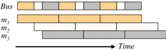
In this section, the test architecture that enables concur- rency of core-based testing using a shared functional bus is discussed. Our general test architecture with buffers similar to [15] is shown in Fig. 1 with the corresponding test delivery and application timing diagram in Fig. 2. In the figures, stage 1 (also labeled Bus) represents the time sharing stage of data delivery through the functional bus to the buffers. The test data in the buffer are subsequently scanned into the scan chains of core (or module)miin stage 2 (also labeledmi).
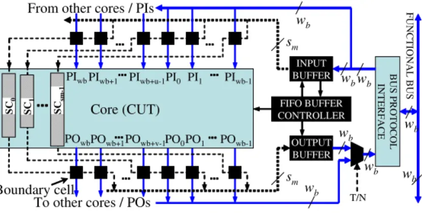
Figure 3 shows the detailed architecture of the interface between the functional bus and the core through the functional bus protocol interface. Both the functional connections (solid lines) and design-for-testability (DFT) connections (dotted lines) are shown. The components in solid black are the proposed buffer-based DFT architecture. The test data are delivered to the input buffer and then scanned into the scan
Bus m1 m2 m3
Time
Fig. 2. Test delivery and application
chains. At the same time, the test responses are scanned out and stored in the output buffer before being retrieved by the test processor for analysis. The scan chains are formed by cascading the input and output boundary cells with the core-internal scan chains with the objective of minimizing the maximum scan chain length.
The buffer consists of four main components as shown in Fig. 4, illustrating the input buffer and the corresponding first- in first-out (FIFO) controller. The output buffer has identical structure as the input buffer, but with reverse data flow. The input register latches data from the bus. Upon registering a full status bit for the input register, the top of the stack copies the data from the input register if its status bit indicates that it is empty. After copying, the input register status bit is cleared, preparing it for the next cycle of data from the bus. The stack will subsequently go through the fall-through stages which will bring the data to the lowest empty slot.
The output register is composed of sm bits, wheresm is the number of wrapper scan chains for module m, possibly differing from the bus width, wb. The output register is interfaced directly to the scan chain inputs. The output register is designed to support this mismatch in bus width and wrapper scan chains. Therefore, it can be easily adapted to any number of scan chains regardless of the bus width.
The test data is serially shifted out from the bottom of the stack, and shifted into the output register. The FIFO buffer controller keeps track of the number of bits being serially shifted into the output buffer,nsi, and the number of bits being serially shifted out of the bottom stack,nso. Serial shifting is clocked by the tri-stated clock signal (labeled !2in Fig. 4 and Fig. 5). Whennsiequalssm, the FIFO controller generates a scan clock !3to scan in the contents of the output buffer into the scan chain, whereupon new data is shifted into the output buffer. When nso equalswb, the FIFO controller generates a control signal !1 to fill in the bottom of the stack with new test data.
The FIFO controller also keeps track of the number of scan clocks already generated. When this number is equal to the longest scan chain in the module,max(lm,i), a capture clock
!4is generated. The FIFO controller can be implemented using three modulo counters, i.e., MOD sm, MOD wb and MOD max(lm,i) as illustrated in Fig. 5. The required input for this circuit isclkin, whose value is the product ofsmand the scan frequency,fm. The same FIFO controller is used for both input and output buffers because of their inverse operation.
The proposed buffer architecture offers two distinct ad- vantages. First, the test application at the module operates
Core (CUT)
PI0 PI1 PIwb-1
wb
PO0PO1 POwb-1 POwbPOwb+1
PIwb+1 PIwb+u-1
wb sm
BUS PROTOCOLINTERFACE
OUTPUT BUFFER
sm
T/N FIFO BUFFER CONTROLLER
From other cores / PIs
To other cores / POs
wb
wb
wb wb
INPUT BUFFER
SC1
SC0 SCsm-1 FUNCTIONAL BUS
Boundary cell
wb wb PIwb
POwb+v-1
Fig. 3. Core test architecture
asynchronously with respect to the availability of test data in the buffer. When empty, the buffer disables the control signal generation by means of status signal α, which is an input to the FIFO controller. Because of the asynchronous scan and capture clock generation by the FIFO controller, the buffer can accommodate unpredictable delivery time of the test vectors, thus handling the synchronization issue. As a result, the scan clock and the bus clock can be decoupled. Such decoupling enables the proposed test mechanism to utilize a bus frequency higher than the scan frequency. Such a capability is lacking in a TAM-based approach because TAM wires are connected directly to the scan chains.
The second advantage is that the buffer allows the test data to be delivered in chunks of any arbitrary multiple of bus width. This flexibility proves to be quite useful in optimizing the test schedule, in addition to minimizing the buffer area overhead.
IV. ALGORITHMICFRAMEWORK
The development of the algorithmic framework—to form a test delivery schedule that minimizes the test application time—addresses two main objectives: minimization of the total required buffer size and maximization of bus utilization while ensuring that all modules receive the test data in a timely manner. In order to satisfy these twin objectives, the buffer
FIFO Buffer Controller
Fall-through stack Input register
Output register Functional bus
Scan chain inputs ε1
α clkin
To core
Bus Protocol Interface
ε2 ε3
ε4
wb 1 2
sm 1 2
wb 12
Fig. 4. Buffer architecture
size and the test delivery sequence need to be optimal. The framework consists of two hierarchical steps. First step (described in Sections IV-B and IV-C) is the grouping of modules which can be tested simultaneously under a maximum power constraint. In the second step (defined in Sections IV-D and IV-E), for each group of modules, the optimum number of packets for every module is determined. Each of these packets is then scheduled for delivery through the functional bus.
In this section, the algorithmic framework is discussed in terms of the two hierarchical steps above. We start by defining a set of nomenclature useful in describing the methodology. A. Terminology
Definition 1: A test packet is composed of a number of bits of test data delivered to a module by the processor, in one burst transfer through the bus.
Definition 2: Due to the delivery of test packets through thewb-bit wide functional bus, the number of bits of test data that makes up a test packet is typically pm×wb, wherepm
is denoted as the packet size for modulem.
Definition 3: A packet set is composed of a series of pack- ets delivered to all modulesmi∈MG, whereMGis the set of all modules in the SOC that are tested simultaneously. Several identical packet sets can be cascaded to form a packet schedule consisting of all packets for all modulesmi to complete the delivery of the test data ofMG.
Definition 4: A modulemi is said to have a split ratio of k, if k packets are scheduled for module miin one packet set. In other words, it means that modulemiwill havek times the number of packets of the smallest modules with a split ratio of one. The module is also called a split-k module.
Scan clock (ε3 ) Capture Clock (ε4 ) Fall-through stack (ε1 )
MOD max(lm,i)
clkin MOD sm
MOD wb Buffer
empty (α )
Serial shift clock (ε2 )
Fig. 5. FIFO buffer controller
m1 m2
m3 m1
m2 m3
Power
Power
Time Time
Pmax
(a) (b)
Fig. 6. Power-constrained scheduling
Definition 5: The scan rate (Rm) is the speed at which the test vectors are loaded into the scan chains and the test responses are shifted out of the scan chains in bits per second (bps). A module with smscan chains andfmscan frequency has a scan rate ofRm =sm×fm.
Definition 6: A test group consists of a subset of modules in an SOC that are tested simultaneously.
B. Effect of Test Frequency Reductions
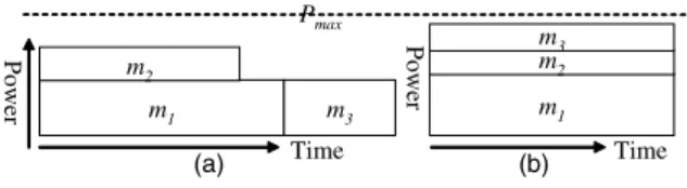
In typical SOC testing, due to the design characteristics such as heat dissipation and current carrying capacity of wires, a limit is imposed on power dissipation that a circuit can tolerate without causing permanent damage to the chip. An illustrative example in Fig. 6(a) shows that module m3
cannot be tested together withm1andm2without exceeding Pmax. However, as shown in Fig. 6(b), if the power-time rectangles form2and m3can be reshaped while keeping the area inside the rectangles constant, all modules can be tested concurrently resulting in shorter total test application time. Further information on the validity of this power-time shape transformation can be found in [8].
C. Algorithm for Forming Test Groups
The ability to greatly simplify the test program when using the systematic packet scheduling methodology (Section IV-E) is one of the primary differentiators of our test methodology. Therefore, when grouping the modules, we utilize a method that supports this novel aspect to ensure that it can be fully exploited—forming non-overlapping test groups.
A test group is formed by scheduling the module with the longest test time first. When scheduling the next module into the same group, its frequency is reassigned to one of the discrete frequencies smaller than the maximum test frequency. The smallest frequency that will not cause the module test time to exceed the test time of the first module in the group is selected as it meets the twin goals of not exceeding the maximum frequency while approaching it maximally within the preset flip-flop quantity constraint for the clock divider circuit. When the largest unscheduled module cannot fit the current group within the power constraint, a module that brings total power dissipation for the group closest to the power limit is chosen. This is repeated until no module can fit in, upon which, the same procedure is repeated to create a new test group.
D. Buffer Sizes
Assuming each packet size ispmi, the buffer size require- ment can be specified as [(packet size in bits) − (number of
bits scanned in during the delivery period of the packet)], or Bmi= (pmi×wb) − ((pmi/fb) × Rmi) (1) Equation (1) holds under the assumption that the next packet is delivered only when the previous packet has already been scanned in completely and the scan in operation can commence once the first bit of data arrives in the buffer. The total buffer size,Btotal, for all modulesmi ∈ M , where M represents all modules in the SOC, is
Btotal= !
mi∈M
Bmi (2)
E. Algorithm for PAcket Set Scheduling (PASS)
The packet scheduling algorithm consists of three steps. The first step consists of determining how to split the test packet for each module so that the individual packet sizes are roughly equal because the largest packet will become the constraint when minimizing the total buffer sizes. In the second step, once the split ratio has been identified, the packet size is determined by solving a set of linear equations. In the third step, a sequence of packet delivery schedules is systematically formed.
Step 1: Let us consider a test group which hasn modules to be tested simultaneously. In the first step of the algorithm, all k < n modules with scan rates smaller than the average scan rate for all modules are considered to have a split ratio of one—the smallest split ratio. This is because other larger modules will be assigned split ratios of larger than or equal to one. Under the PASS scheme, the smallest possible number of packets is desirable when forming a packet set in order to minimize the complexity of the resulting test program.
Before proceeding, we define a relevant terminology to aid the description of the algorithm.
Definition 7: Assuming that the bus delivery rate is suffi- ciently high, a packet set is considered to be in perfect-fit if (i) it does not have modules that are waiting for test data, (ii) there are no two consecutive packets delivered that belong to the same module and (iii) the number of packets between adjacent split-1 packets are equal. Furthermore, all three conditions need still hold when two adjacent perfect-fit packet sets are cascaded, except possibly for the initial or final legs of test application.
In order to ensure perfect-fit criteria is not violated, for any value of r > 1, such that k mod r is zero, the number of split-r modules must equal d × k/r for some positive integer d, in order to form a perfect-fit packet set consisting of split-1 and split-r modules. That is because in order to have an even utilization of bus time, as outlined in condition (iii) of Definition 7, we need to schedule the same number of split-r packets in between the delivery of split-1 packets. This formsd subgroups of (k/r) split-r modules which make up the split-r group.
To determine the split-r modules, we iteratively check for all possible values ofr, starting with the smallest. Let Ravg
be the average scan rate of split-1 modules. For the remaining modules with split ratio value unassigned, if there existk/r
1
p1,1 2
p1,1 3
p2,1 p32,2
4
p4,1 p4,24 p4,34 p4,44 m1: split-1
m2: split-1 m3: split-2 m4: split-4
tstart tend
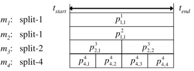
Fig. 7. Packet TAT and split ratio
modulesmi that fulfill Rmi< βr × Ravg for some constant β, then all thek/r modules are assigned split ratio values of r. The constant β gives a cut-off limit on the largest module to be assigned to split-r group. It limits the relative buffer sizes of split-r modules and split-1 modules. The value of β = 1.5 was chosen after thorough experimentation.
The process above is repeated when identifying the nextk/r subgroups of split-r modules. As a result, d subgroups of k/r modules are assigned the split ratio ofr. If no subgroup could be found for the current value ofr, this process is repeated for the next larger value ofr until r equals k. Then, the remaining (n − k − d × k/r) modules are assigned a split ratio of 2k to form the split-2k group.
Instead of assigning split ratio of 2k for the remaining modules, the same procedure for forming the split-r group can be extended to form other split groups. However, to minimize the algorithm complexity, we have chosen only three split ratio values (k, r, and 2k) since they provide sufficiently good results as illustrated in Section V.
Step 2: Once the split ratios are determined, the next step is to determine the packet size for each module. Equation (3) describes the scan in time of a test packet, wherewbis the bus width, andpmi and fmi the packet size and scan frequency, respectively, for modulemi.
Tmi,p= wb×pmi/fmi (3) To preclude introduction of gaps between the test applica- tions of two consecutive packets of a module as illustrated by Fig. 2, the packet TATs multiplied by the corresponding split ratio must be identical as illustrated by Fig. 7. Equation (4) describes the packet TAT as illustrated by Fig. 7, where r and 2k are the corresponding split ratios for each module. Packet size, pmi, and buffer size, Bmi, for each module mi can be calculated by solving equations (1), (2), and (4) simultaneously. For each value of Btotal, a unique solution can be obtained.
Step 3: The complete packet set schedule can be system- atically represented by Fig. 8, assumingk and q modules for split-1 and split-2k groups, respectively. Each pgi,j represents a test packet delivery and response packet retrieval where,
g = module number from split-i group i = split ratio for module g
j = packet number for module g, and j ≤ i
Figure 8 shows the sequence of packet delivery for one packet set that fulfils the perfect-fit condition in Definition 7.
1 ( 1) / 1 /
1 2 1
2 ,1 2 ,1 2 ,1 ,1 ,1 ,1
1 2 1
2 ,2 2 ,2 2 ,2 1,1
2 ( 1) / 2 /
1 2 2
2 ,3 2 ,3 2 ,3 ,1 ,1 ,1
1 2 2
2 ,4 2 ,4 2 ,4 1,1
/ / /
1 2
2 ,2 1 2 ,2 1 2 ,2 1 , ,
...
...
..
q k r d k r
k k k r r r
q
k k k
q k r d k r
k k k r r r
q
k k k
q k r k r k r
k k k k k k r r r r
p p p p p p
p p p p
p p p p p p
p p p p
p p p p p
+ − +
+ − +
+
− − −
/ ( 1) / ,
1 2
2 ,2 2 ,2 2 ,2 1,1
. r rk r d k r
q k
k k k k k k
p
p p p p
+ −
Fig. 8. Packet set delivery sequence
In Fig. 8, the odd rows (horizontal) show the schedule delivery forq split-2k packets followed by d split-r packets. The even lines show the schedule delivery for the subsequentq split-2k packets followed by a single split-1 packet from one of thek modules.
The retrieval of the response packet is scheduled after every test packet delivery. This approach requires minimal overhead on the control algorithm specified by the packet set in Fig. 8. This differs from the TAM approaches, where test data delivery and response retrieval are performed simultaneously at the expense though of doubling the number of physical pins on the chip.
V. EXPERIMENTALRESULTS
In order to evaluate our methodology, we have conducted experiments on several ITC’02 benchmark [17] circuits. Power dissipation information is not available in the benchmark suite definition. However, we obtained power information for p93791 and p22810 from [7] and d695 from [6]. In order to analyze the utilization of functional bus for test data delivery, a single shared functional bus is assumed to be connected to every module. Additionally, an embedded processor (in addition to the cores originally defined by the benchmark suite) is assumed connected to the functional bus.
Figure 9 illustrates the effect of the frequency divider resolution on the test application time. In each plot, the bottom curve is the test time after the test group has been formed under a power constraint. The higher frequency divider resolution allows us to achieve a shorter test application time. A significant reduction in test time can be achieved within the first four bits of clock divider resolution. The packet scheduling test time (top curves) are always higher as they incur an additional overhead when splitting the test data into smaller packets.
p93791
10 11 12 13 14 15 16
1 2 3 4 5 6 7 8 9 10
#FF in fre que ncy divide r
TAT
d695
0.4 0.5 0.5 0.6 0.6 0.7
1 2 3 4 5 6 7 8 9 10
#FF in fre que ncy divide r
TAT
Fig. 9. Frequency divider resolution
wb· pm1
fm1
= · · · = wb· pmk fmk
= r ·wb· pmk+1 fmk+1
= · · · = r ·
wb· pmk+ dk r
fmk+ dk r
= 2k ·
wb· pmk+ dk r+1
fmk+ dk r+1
= · · · = 2k ·
wb· pmk+ dk r+q
fmk+ dk r+q
(4)
TABLE I
SCAN AND BUS FREQUENCY SETTINGS
Scan frequency Bus frequency TAM-based fs=Fs fb=fs< Fb
PASSa fs=Fs fb=fs< Fb
PASSb fs=Fs fb= 2 ×fs< Fb
In order to evaluate the performance of our test scheme, we need to compare with TAM-based test scheduling approaches. No direct comparison can be offered with previous functional test schemes as the experimental results in [15] used four benchmark circuits which do not have the required information such as information on test data and scan chain configurations that are needed. Table I shows the frequency information for TAM approaches and two variations of our approaches, PASSa and PASSb, with distinct bus frequencies1.
Figure 10 shows plots of the TAT for different bus widths. For 64- to 128-bit bus, the TAT is constrained by the largest module; therefore, adding bus widths has no significant effect on test application time. However, for bus widths between 12 and 48 bits, PASSa delivers improvements of 4.8% and 18.2% over [7] for both maximum power,Pmax, values of 3,000 and 10,000 for p22810. PASSb is improved by 25.9% to 47.8% when test data delivery time is the limiting factor. Similar trends can be observed for p93791 in Fig. 10(c) and Fig. 10(d). In fact, our test methodology delivers marked improvements in reducing test application time for smaller bus widths.
1The scan frequency, fs, is set to the assumed maximum, Fs= 100 MHz; therefore all the TAM-based TATs are divided by 105 to convert from the number of clock cycles to time (millisecond). The bus frequency, fb, for PASSb is double that of TAM-based and PASSa approaches (but less than the maximum bus operating frequency, Fb) to illustrate the benefit of our buffer-based approach.
p22810 @ Pmax = 10000
0 2 4 6 8 10 12 14
12 16 20 24 32 48 64 80 96 112 128Bus W idth
TAT
[7] PASSa PASSb
(b)
p22810 @ Pmax = 3000
0 2 4 6 8 10 12 14
12 16 20 24 32 48 64 80 96 112 128
Bus W idth
TAT
[7] PASSa PASSb
(a)
p93791 @ Pmax = 20,000
0 10 20 30 40 50 60 70
12 16 20 24 32 48 64 80 96 112 128Bus W idth
TAT [7]
PASSa PASSb
(d)
p93791 @ Pmax = 10,000
0 10 20 30 40 50 60 70
12 16 20 24 32 48 64 80 96 112 128Bus W idth
TAT [7]PASSa
PASSb
(c)
Fig. 10. Test application time vs. bus width
0 2 4 6 8 10 12 14
30 40 50 60 70 80 90 100
Total Buffer Size
TAT
p93791, Pmax=10000 p93791, Pmax=20000 p22810, Pmax=10000 p22810, Pmax=3000
Fig. 11. Buffer size vs. TAT
For d695 (Table II), our approach proves to be highly effective, even for the same bus frequency as [6], [7], at all power levels for bus widths ranging from 32 to 80 bits. For 96-bit and wider buses, our methodology though fails to perform as well. It is interesting to note, however, that the TAM-based approach requires quite elevated levels of TAM overhead in order to outperform our packet scheduling approach, which is utilizing the existing functional bus.
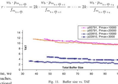
Figure 11 shows the trend in TAT under different buffer size utilization for the two circuits with the same power constraints as in Fig. 10 and for 32-bit bus. The buffer size represents the total size, in multiples of bus width, allocated to all modules in the circuit. It is interesting to note that increasing buffer size only reduces TAT marginally. Therefore, buffer size can be reduced with only a small penalty on TAT. For all the experiments reported, the maximum total buffer size constraint is100 × wbbits.
With the flexibility of bus frequency selections, unique to our proposed approach as a TAM-based approach is unable to utilize such flexibility, we can further improve the TAT
TABLE II
TEST APPLICATION TIME(D695)
[6] [7] PASSa PASSb [6] [7] PASSa PASSb
1500 0.456 0.435 0.405 0.246 0.276 0.270 0.245 0.238 1800 0.443 0.425 0.370 0.189 0.245 0.239 0.188 0.171 2000 0.432 0.425 0.371 0.193 0.242 0.219 0.193 0.191 2500 0.432 0.418 0.373 0.188 0.237 0.219 0.188 0.135
1500 0.209 0.244 0.237 0.238 0.209 0.234 0.233 0.232 1800 0.205 0.188 0.172 0.169 0.181 0.188 0.170 0.169 2000 0.192 0.187 0.180 0.185 0.178 0.175 0.181 0.178 2500 0.192 0.187 0.153 0.133 0.158 0.173 0.138 0.137
1500 0.168 0.194 0.240 0.237 0.168 0.194 0.233 0.231 1800 0.150 0.188 0.169 0.170 0.149 0.168 0.169 0.168 2000 0.141 0.146 0.180 0.187 0.141 0.145 0.179 0.179 2500 0.141 0.140 0.136 0.136 0.130 0.134 0.135 0.135
Bus = 112 Bus = 128
Pmax
Bus = 32 Bus = 64
Bus = 80 Bus = 96
while ensuring that nothing more than minimal bus widths are utilized. This is illustrated in Fig. 10 and Table II by PASSb, whose bus frequency is twice that of the TAM-based and PASSa approaches; the scan frequency is the same.
VI. CONCLUSION
The utilization of the functional bus for power-constrained core-based SOC testing entails a number of challenges. These include frequency and bit-width mismatch between the bus and the modules under test, allocation of bus time slots for an efficient test data delivery schedule that maximizes bus utilization and that ensures that all modules always have the test data that they need to continue testing simultaneously without exceeding the power constraint.
We have herein proposed an efficient methodology that overcomes all of these challenges through a test support ar- chitecture design framework and an algorithmic design frame- work. The proposed methodology offers a solution that also minimizes the size of the test program. The experimental data clearly showcases the benefits of the proposed methodology in reducing test application time especially for smaller bus widths, while also eliminating the need to add extraneous TAMs to the SOC solely for testing purposes.
ACKNOWLEDGMENTS
This work was supported in part by 21st Century COE (Center of Excellence) Program (Ubiquitous Networked Media Computing) and in part by Japan Society for the Promo- tion of Science (JSPS) under Grants-in-Aid for Scientific Research B(2) (No.15300018) and for Young Scientists (B) (No.18700046).
REFERENCES
[1] Erik Jan Marinissen, Rohit Kapur, Maurice Lousberg, Teresa McLau- rin, Mike Ricchetti, and Yervant Zorian, “On IEEE P1500 Standard for Embedded Core Test,” Journal of Electronic Testing: Theory and Applications, 2002, pp. 365-383.
[2] Erik Jan Marinissen, Robert Arendsen, Gerard Bos, Hans Dingemanse, Maurice Lousberg, and Clemens Wouters, “A Structured and Scalable Mechanism for Test Access to Embedded Reusable Cores,” In Proc. International Test Conference 1998, pp. 284-293.
[3] Toshinobu Ono, Kazuo Wakui, Hitoshi Hikima, Yoshiyuki Nakamura, and Masaaki Yoshida, “Integrated and Automated Design-for-Testability Implementation for Cell-based ICs,” In Proc. 6thAsian Test Symposium 1997, pp. 122-125.
[4] Anuja Sehgal, Vikram Iyengar, Mark D. Krasniewski, and Krishnendu Chakrabarty, “Test Cost Reduction for SOCs Using Virtual TAMs and Lagrange Multipliers,” In Proc. 40th Design Automation Conference 2003, pp. 738-743.
[5] Mohsen Nahvi and Andr´e Ivanov, “A Packet Switching Communication- Based Test Access Mechanism for System Chips,” In Proc. IEEE Euro- pean Test Workshop, 2001, pp. 81-86.
[6] Yu Huang, Sudakhar M. Reddy, Wu-Tung Cheng, Paul Reuter, Nilanjan Mukherjee, Chien-Chung Tsai, Omer Samman, and Yahya Zaidan, “Op- timal Core Wrapper Width Selection and SOC Test Scheduling Based on 3-D Bin Packing Algorithm,” In Proc. International Test Conference 2002, pp. 74-82.
[7] Julien Pouget, Erik Larsson, and Zebo Peng, “Multiple-Constraint Driven System-on-Chip Test Time Optimization,” Journal of Electronic Testing: Theory and Applications, Vol. 21, 2005, pp. 599-611.
[8] Tomokazu Yoneda, Kimihiko Masuda, and Hideo Fujiwara, “Power- Constrained Test Scheduling for Multi-Clock Domain SOCs”, In Proc. Design, Automation and Test in Europe 2006, pp. 297-302.
[9] Peter Harrod, “Testing Reusable IP - A Case Study,” In Proc. International Test Conference 1999, pp. 493-498.
[10] Angela Krstic, Li Chen, Wei-Cheng Lai, Kwang-Ting Cheng, and Sujit Dey, “Embedded Software-Based Self-Test for Programmable Core-Based Designs”, IEEE Design & Test of Computers, Vol. 19, Issue 4, July/Aug. 2002, pp. 18-27.
[11] Christos A. Papachristou, F. Martin, and Mehrdad Nourani, “Micropro- cessor Based Testing for Core-Based System on Chip,” In Proc. IEEE Design Automation Conference 1999, pp. 586-591.
[12] Li Chen and Sujit Dey, “Software-Based Self-Testing Methodology for Processor Cores,” IEEE Transactions On Computer-Aided Design Of Integrated Circuits And Systems, Vol. 20, No. 3, 2001, pp. 369-380. [13] Rochit Rajsuman, “Design and Test of Large Embedded Memories: An
Overview,” IEEE Design & Test of Computers, Vol. 18, Issue 3, May/June 2001, pp. 16-27.
[14] Jing-Reng Huang, Madhu K. Iyer, and Kwang-Ting Cheng, “A Self-Test Methodology for IP Cores in Bus-Based Programmable SOCs,” In Proc. VLSI Test Symposium 2001, pp. 198-203.
[15] Anders Larsson, Erik Larsson, Petru Eles, and Zebo Peng, “Optimization of a Bus-based Test Data Transportation Mechanism in System-on-Chip”, In Proc. 8thEuromicro Conference on Digital Systems Design, 2005, pp. 403-411.
[16] Antonis M. Paschalis, Dimitris Gizopoulos, Nektarios Kranitis, Mihalis Psarakis, and Yervant Zorian, “Deterministic Software-Based Self-Testing of Embedded Processor Cores”, In Proc. Design, Automation & Test in Europe 2001, pp. 92-96.
[17] Erik Jan Marinissen, Vikram Iyengar, and Krishnendu Chakrabarty, “A Set of Benchmarks for Modular Testing of SOCs”, In Proc. International Test Conference 2002, pp. 519-528.