Design for Consecutive Testability of Systems-on-a-Chip
with Built-In Self Testable Cores
Tomokazu Yoneda and Hideo Fujiwara
Graduate School of Information Science, Nara Institute of Science and Technology 8916-5 Takayama, Ikoma, Nara, 630-0101, Japan
Tel : +81-743-72-5226 Fax : +81-743-72-5229 tomoka-y, fujiwara @is.aist-nara.ac.jp
Abstract
This paper introduces a new concept of testability called consecutive testability and proposes a design-for-testability method for making a given SoC consecutively testable based on integer programming problem. For a consecu- tively testable SoC, testing can be performed as follows. Test patterns of a core are propagated to the core inputs from test pattern sources (implemented either off-chip or on-chip) consecutively at speed of system clock. Similarly the test responses are propagated to test response sinks (im- plemented either off-chip or on-chip) from the core outputs consecutively at speed of system clock. The propagation of test patterns and responses is achieved by using the con- secutive transparency properties of surrounding cores and interconnects between cores. All interconnects can be tested in a similar fashion. Therefore, it is possible to test not only logic faults such as stuck-at faults but also timing faults such as delay faults that require consecutive application of test patterns at speed of system clock.
keywords: consecutive testability, consecutive trans- parency, test access mechanism, systems-on-a-chip, design for testability, built-in self test
1 Introduction
A fundamental change has taken place in the way digital systems are designed. It has become possible to design an entire system, containing millions of transistors, on a single chip. In order to cope with the growing complexity of such modern systems, designers often use pre-designed, reusable megacells knows as cores. Core-based systems-on-a-chip (SoC) design strategies help companies significantly reduce the time-to-market and design cost for their new products.
However, SoCs are difficult to test after fabrication[1]. In order to make SoC testable, the following three condi- tions have to be satisfied. (1)There exist test pattern source (TPS) and test response sink (TRS) for each core. The TPS generates the test patterns for the embedded core, and the TRS observes the test responses. TPS as well as TRS can
be implemented either off-chip or on-chip. (2)There ex- ists test access mechanism for each core. The test access mechanism propagates test patterns and responses. It can be used for on-chip propagation of test patterns from a TPS to the core-under-test, and for on-chip propagation of test responses from the core-under-test to a TRS. (3)Intercon- nects that exist between cores are testable.
A major difficulty to make SoC testable concerns ac- cessibility of embedded cores. Several techniques of design-for-testability (DFT) have been proposed. There are three main approaches to achieve accessibility of em- bedded cores. The first approach is based on test bus architectures[2, 3, 4]. The second approach is based on boundary scan architectures[5, 6]. The third approach uses transparency[8, 9, 10] or bypass mode[7] for embedded cores to propagate test patterns and responses.
Under the design environment for SoCs, it is also impor- tant to test timing faults such as delay faults as well as logic faults such as stuck-at faults. For that reason, it is neces- sary to be capable of applying test patterns and observing the responses consecutively at speed of system clock. We call such a test access consecutive test access. Although test bus approach is consecutively test accessible, it is difficult to test interconnects. On the other hand, boundary scan, transparency, and bypass mode approaches are able to test interconnects, they are not consecutively test accessible.
In [11], assuming that TPS and TRS are implemented only off-chip (i.e., embedded cores are tested by using ex- ternal automatic test equipment), we proposed a new testa- bility of SoCs called consecutive testability. A consec- utively testable SoC consists of consecutively transparent cores only and can achieve consecutive test access to all cores and all interconnects.
In this paper, we consider SoCs that include BISTed (Built-In Self Tested) cores and opaque cores as well as non-BISTed cores and consecutively transparent cores, and extend the concept of consecutive testability of SoCs so that TPS and TRS implemented both on-chip and off-chip can be dealt with. Then, we present a DFT method to make IEEE 2001 Workshop on RTL ATPG & DFT, pp. 28-37, Nov. 2001.
a given SoC consecutively testable. Consecutive testabil- ity of an SoC guarantees that, for each core (for each in- terconnect), by using consecutive transparencies of other cores and interconnects, test patterns can be fed into the core (the interconnect, respectively) from TPS and the responses can be propagated to TRS consecutively at speed of system clock. Therefore, consecutively testable SoCs can achieve high quality of test since any test sequence for a core can be applied to the core from TPS and any response sequence can be observed at TRS consecutively at speed of system clock.
This paper is organized as follows. In section 2, we intro- duce an SoC model. In section 3, we introduce the consec- utive transparency, the consecutive testability, and present a new test methodology for testing SoCs. In section 4, we present a graph model for an SoC. In section 5, we present a DFT method for consecutive testability. Section 6 con- cludes this paper.
2 Systems-on-a-Chip
An SoC consists of hardware elements and intercon- nects. A hardware element is a primary input (PI), a pri- mary output (PO), or a core. For the sake of uniformity, user-defined logic can be considered as another core. Each individual core is testable by either external test or built-in self test. In case a core is testable by external test, a pre- computed test set is available for the core which, if applied to the core, will result in a very high fault coverage. We in- troduce ports of each hardware element as interface points in a natural fashion: signals enter into a hardware element through its input ports, and exit through its output ports. For convenience, we regard a PI as an output port and a PO as an input port. An interconnect connects an output port with an input port. Any number of interconnects can connect to the same output port (i.e., fanout is allowed), but only one interconnect can connect to the same input port. It is not necessary that interconnects are of the same bit width. 3 A Test Methodology for Systems-on-a-Chip
Based on Consecutive Testability
We present a new test methodology for SoCs based on consecutive testability. Figure 2 illustrates a consecutively testable SoC and the consecutive test access to Core 3. A control signal is provided for each core by a test controller (either off-chip or on-chip). Each control signal of a core determines the current test mode of the core called a config- uration. The types of configurations are consecutive trans- parencies and functions as a TPS and a TRS. Core 1 works as a TPS for Core 3. Core 2 realizes a consecutive trans- parency of shaded output port and Core 4 realizes a con- secutive transparency of shaded input port. Consecutive
core2
core3
core4
core7 core6
core8 core5 core1
core9 Primary Inputs
Primary Outputs
Figure 1. Systems-on-a-Chip
transparency of an input port guarantees that any input se- quence applied to the input port can propagate to some out- put ports consecutively at speed of system clock, and con- secutive transparency of an output port guarantees that any output sequence that appears at the output port can propa- gate from some input ports consecutively at speed of system clock. Consecutive testability of an SoC guarantees that, for each core (for each interconnect) in the SoC, by selecting configurations of other cores, any test sequence can be con- secutively fed into the core (the interconnect, respectively) from TPSs and any response sequence can be consecutively propagated to TRSs through consecutive transparencies of other cores and interconnects. We define the consecutive transparency of a core and the consecutive testability of an SoC in the following subsections.
3.1 Consecutive Transparency of a Core Definition 1: Consecutive transparency of a core
Let I i be the ith bit of an input port I, and O j be the jth bit of an output port O. Suppose that there exists a configuration of a core which can realize a path P between I i and O j . P is called a consecutively transparent path if any input sequence applied to I i can be consecutively observed at O j after some latency, and then I i and O j are said to be consecutively transparent. Moreover, a core is called to be consecutively transparent if, for each port of the core, there exists a configuration that can make all bits of the port consecutively transparent.
Figure 3 illustrates various configurations of a consec- utively transparent core. A consecutively transparent core has generally several configurations, and each configuration can be identified by an ID number. By selecting a config- uration of a core, consecutively transparent paths of an I/O port are realized and the I/O port can be made consecutively transparent. For each configuration, all consecutively trans-
CUT
Test Sequence
time t : vector1 Test Sequence
time t +2 : response2 time t +1 : response1
time t +1+ m : response1 PO
PI
Test Controller
selected consecutive transparency not selected consecutive transparency
latency: k cycles
latency: m cycles time t +2 - k : vector3 time t +1 - k : vector2 time t - k : vector1
time t +2 : vector3’ time t +1 : vector2’ time t : vector1’
Test Response Core 1
Core 2
Core 3
Core 4
TPS
TPS
TRS
Figure 2. Consecutive Test Access
parent paths between an input port and an output port are represented as one consecutively transparent path.
We classify consecutively transparent paths into three types, PA (Propagation AND), PO (Propagation OR), and JA(Justification AND). PA and PO are types of consecu- tively transparent paths for input ports to propagate test re- sponses. JA is a type of consecutively transparent paths for output ports to justify test sequences. Figure 3(a) illustrates type PA such that any input sequence applied to an input port I1propagates to only one output port O2. Figure 3(b) illustrates type PA such that any input sequence applied to an input port I2propagates to two output ports(O1and O2), where any input sequence of bit width W I2 is bit-sliced (W I2 w2 w3) and observed at two output ports (O1
and O2). Figure 3(c) illustrates type PO such that any in- put sequence applied to I3 propagates to two output ports (O1and O2), where any input sequence of bit width W I3
is fanouted (W I3 w4 w5) and observed at two output ports (O1and O2).
3.2 Test Pattern Source and Test Response Sink The test pattern source (TPS) generates test patterns for cores and interconnects, and the test response sink (TRS) observe the test responses. TPS and TRS can be imple- mented either off-chip or on-chip. In this paper, we classify TPS and TRS into the following three types (Figure 4).
1. SBIST
SBIST is a type of TPS and TRS implemented inside of
w1 w2 w3 w4 w5
w6 I1
w7 w8
(a) Configuration ID 1 (b) Configuration ID 2 (c) Configuration ID 3
(d) Configuration ID 4 (e) Configuration ID 5 PA
JA
PO PA
PA PO
JA JA
W(Ii) : bitwidth of an input port Ii W(Oi) : bitwidth of an output port Oi wi : bitwidth of consecutive transparent path
I2 I3
O1 O2
I1
I2 I3
O1 O2
I1
I2 I3
O1 O2
I1
I2 I3
O1 O2
I1
I2 I3
O1 O2
W(I1) = w1 W(I2) = w2 + w3 W(I3) = w4 = w5
W(O2) = w7 + w8 W(O1) = w6
Figure 3. Various Configurations of a Consecu- tively Transparent Core
a core (i.e.,on-chip) and used for testing the core itself (Figure 4(c)). A core which has this type of TPS and TRS can be self-testable.
2. So f f
So f f is a type of TPS and TRS implemented off-chip by external automatic test equipment (Figure 4(a)). TPS of type So f f can generate any test sequence of any length, and TRS of type So f f can observe any re- sponse sequence of any length consecutively at speed of system clock.
3. Son
Sonis a type of TPS and TRS implemented inside of a core (i.e.,on-chip) and used for testing other cores (Fig- ure 4(b)). Since TPS and TRS of type Sonare imple- mented on-chip, memory spaces for them are limited. Therefore, TPS and TRS of type Son cannot deal with arbitrary long sequences like TPS and TRS of type So f f. However, within the limited memory spaces, TPS of type Son can generate any test sequence and TRS of type Son can observe any response sequence consecutively at speed of system clock. A core which can be tested by TPS and TRS of type Soncan be also tested by TPS and TRS of type So f f. A core which has TPS and TRS of type Son has several configurations (Figure 5), and each configuration can be identified by an ID number. By selecting a configuration of the core, the core can realize functions as a TPS and a TRS. 3.3 Consecutive Testability of a System-on-a-Chip
In this subsection, we introduce a new testability of an SoC called consecutive testability. In this paper, we assume that the following informations are given as an SoC.
Connectivity information between cores Test informations of each core
CUT SoC
TRS
CUT SoC CUT
SoC
(a) Soff (b) Son (c) SBIST TRS
TPS
TRS TPS
TPS
Figure 4. Types of TPS and TRS
– type of TPS/TRS that can test the core (SBIST or So f f or Son)
– configurations if the core is consecutively trans- parent
– configurations if the core has TPS/TRS of type Son
The length of a test sequence required to test an in- terconnect is usually much shorter than that required to test a core. Hence, we assume all interconnect can be tested by TPS/TRS of type Son. In order to test a core, it is necessary to apply test patterns consecutively to all input ports of the core simultaneously. On the other hand, it is not necessary to observe all output ports of the core simultaneously. It is sufficient only to observe one output port at a time. Therefore, we define the consecutive test accessibility of a core and the consecutive test accessibility of an interconnect as follows.
Definition 2: Consecutive test accessibility of a core A core C is said to be consecutively test accessible if the following two conditions are satisfied at the same time for each output port O of C.
1. Any test sequence generated by the TPS required to test C can be applied to all input ports of C consecu- tively at normal system clock (consecutive controlla- bility of C for TPS).
2. Any response sequence appeared at O can be propa- gated to the TRS required to test C consecutively at normal system clock (consecutive observability of O for TRS).
Definition 3: Consecutive test accessibility of an intercon- nect
For an interconnect E that connects an output port O with an input port I, E is said to be consecutively test accessible if O and I satisfies the following two conditions at the same time.
W9 (a) Son
(d)Configuration ID 8 (b) Configuration ID 6 (c) Configuration ID 7
JA O1 O2
I3 W(O1) = W9
O1 O2
O1 O2 O1 O2
TRS
TPS
I1
I2 I3
TPS
W10 JA
TPS
W(O2) = W10 W11 PA
TRS W(I3) = W11 W(Ii) : bitwidth of an input port Ii W(Oi) : bitwidth of an output port Oi wi : bitwidth of consecutive transparent path
Figure 5. Various Configurations of a Core that has TPS and TRS of typeSon
1. Any test sequence generated by the TPS required to test E can be applied to O consecutively at normal sys- tem clock (consecutive controllability of E for TPS). 2. Any response sequence appeared at I can be propa- gated to the TRS required to test E consecutively at normal system clock (consecutive observability of I for TRS).
Then, we define the consecutive testability of an SoC as follows.
Definition 4: Consecutive testability of an SoC
An SoC is said to be consecutively testable if all cores and all interconnects in the SoC are consecutively test accessible.
4 Graph Modeling
In this section, we define a core connectivity graph to represent an SoC, and consider the consecutive testability on the graph.
Definition 5: Core connectivity graph
We define a core connectivity graph G V E λ as a fol- lowing directed graph to represent an SoC.
V VPI VPO Vin Voutwhere VPIis the set of all PIs of the SoC, VPOis the set of all POs of the SoC,
Vinis the set of all input ports of cores in the SoC, and Voutis the set of all output ports of cores in the SoC. E Ecore Enet where
Ecore x y Vin Vout input port x is connected to output port y by a consecutively transparent path ,
c2 c1
c3
c4
c6
c5
c7
c8 c9
Figure 6. Core Connectivity Graph
and
Enet y x Vout Vin output port y is connected to input port x by an interconnect .
Labeling functionλ : E 2C I T Wwhere Cis the set of all cores in the SoC,
Iis the set of all ID numbers of configurations, T JA JO PA PO types of consecutively transpar- ent path (JO is for fanouted interconnects) , and Wis the set of all bit widths of e E.
Especially for e Enet,
λ e φ φ JO bit width of e φ φ PO bit width of e
Figure 6 illustrates a core connectivity graph G which corresponds to the SoC of Figure 1. Figure 7 illustrates edges labeled byλ which correspond to the core of Figures 3 and 5.
We refer to a vertex that has no input edge as a source, and a vertex that has no output edge as a sink. For a core connectivity graph G, selecting a configuration of a core is to leave edges which have labels of the configuration and to remove other edges from the core.
Then, we define a justification subgraph of a core, a justification subgraph of an interconnect and a propagation subgraph of a port as subgraphs of a core connectivity graph.
Definition 6: Justification subgraph of a core
Let G V E λ be a core connectivity graph of an SoC and GJ VJ EJ λ be an acyclic subgraph of G. For a core c C, GJis called a justification subgraph of c if GJ
satisfies all the following conditions.
1. All input ports of c are sinks in GJand there exists no sink except for all input ports of c in GJ.
2. For each edge u EJ, u has a label of either JO or JA.
e1 e2 e3
e4 e5
e1 : {{c, 2, PA, w2}, {c, 4, JA, w6}} e2 : {{c, 2, PA, w3}}
e3 : {{c, 1, PA, w1}, {c, 5, JA, w7}} e4 : {{c, 3, PO, w4}}
e5 : {{c, 3, PO, w5}, {c, 5, JA, w8}} e6 : {{c, 6, JA, w9}}
e7 : {{c, 7, JA, w10}} e8 : {{c, 8, PA, w11}} e8
e7 e6
O1 O2
I1
I2 I3
Figure 7. Label byλ
3. Let G V E λ be a subgraph of G obtained by selecting a configuration for each core. For each edge u EJ,
(a) u contains all input edges of u in G , and (b) u contains only one output edge of u in G when
output edges have labels of JO in G .
Lemma 1: Let VSbe the set of all source vertices in GJof core c. Then c is consecutively controllable for VS
proof: By Definition 5 and condition 2 of Definition 6, all edges in GJcan be used to apply test patterns consecutively at speed of system clock since each edge in GJ represents either a consecutively transparent path or an interconnect, and has a label of either JO or JA. By condition 1 of Defini- tion 6, there exist simple paths from more than one element in VSto each input port of c. By condition 3 of Definition 6, all edges in the same core have the same ID number of configuration since only one configuration is selected for each core. Let v be the vertex in Vout (i.e., v is an output port of a core). If a configuration to realize a consecutive transparency of v is selected, all consecutively transparent paths for v exist in GJ(condition 3(a) of Definition 6). If a configuration to realize a consecutive transparency of v is not selected, v is a source vertex in GJ. By condition 3(b) of Definition 6, it is possible to apply any test sequence for all simple paths at the same time.
Therefore, we can see that any test sequence generated at VScan be applied to all input ports of c along all simple paths in GJconsecutively at speed of system clock. Hence, the Lemma is proved.
Definition 7: Justification subgraph of an interconnect Let G V E λ be a core connectivity graph of an SoC and GJ VJ EJ λ be an acyclic subgraph of G. For an in- terconnect e y x Enet, GJis called a justification sub- graph of eif GJsatisfies all the following conditions.
1. Only y is a sink in GJ.
2. For each edge u EJ, u has a label of either JO or JA. 3. Let G V E λ be a subgraph of G obtained by selecting a configuration for each core. For each edge
u EJ,
(a) u contains all input edges of u in G , and (b) u contains only one output edge of u in G when
output edges have labels of JO in G .
Lemma 2: Let VSbe the set of all source vertices in GJof interconnect e. Then e is consecutively controllable for VS
proof:The Lemma is proved similarly to Lemma 1. Definition 8: Propagation subgraph of a port
Let G V E λ be a core connectivity graph of an SoC and GP VP EP λ be an acyclic subgraph of G. For a vertex v V, GPis called propagation subgraph of v if GP
satisfies all the following conditions. 1. Only v is a source in GP.
2. For each edge u EP, u has a label of either PO or PA. 3. Let G V E λ be a subgraph of G obtained by selecting a configuration for each core. For each edge u EP,
(a) u contains all output edges of u in G when the output edges have labels of PA, and
(b) u contains more than one output edge of u in G when the output edges have labels of PO in G .
Lemma 3: Let VE be the set of all sink vertices in GP of vertex v. Then v is consecutively observable for VE
proof: By Definition 8 and condition 2 of Definition 6, all edges in GP can be used to propagate test responses con- secutively at speed of system clock since each edge in GP
represents either a consecutively transparent path or an in- terconnect, and has a label of either PO or PA. By condition 1 of Definition 8, there exist simple paths from v to each element in VE. By condition 3 of Definition 8, all edges in the same core have the same ID number of configuration since only one configuration is selected for each core. Let v be the vertex in Vin (i.e., v is an input port of a core). If a configuration to realize a consecutive transparency of v is selected and the consecutively transparent paths for v are type PA, all consecutively transparent paths for v exist in GP(condition 3(a) of Definition 8). If a configuration to realize a consecutive transparency of v is selected and the consecutively transparent paths for v are type PO, there ex- ist at least one consecutively transparent path for v in GP
(condition 3(b) of Definition 8). If a configuration to realize a consecutive transparency of v is not selected, v is a sink vertex in GP.
Therefor, we conclude that any response sequence appeared at v can be propagate to VEalong all simple paths
in GP consecutively at speed of system clock. Hence, the Lemma is proved.
Theorem 1: Let G V E λ be a core connectivity graph of an SoC. An SoC is said to be consecutively testable if the SoC satisfies the following two conditions.
1. For each output port v Voutof each core c C, there exist one justification subgraph GJof c and one propa- gation subgraph GPof v where GJand GPare disjoint and satisfy the following conditions.
if TPS/TRS type required to test c is SBIST
GJ GP φ
if TPS/TRS type required to test c is So f f
VS VPI VE VPO
if TPS/TRS type required to test c is Son
VS VPI Vsource VE VPO Vsink
2. For each interconnect e y x Enet, there exist one justification subgraph GJ of e and one propagation subgraph GP of x where GJand GP are disjoint and satisfy the following conditions.
VS VPI Vsource VE VPO Vsink
proof: The Theorem is proved by Definitions 2, 3, 4 and Lemmas 1, 2, 3.
5 DFT for Consecutive Testability
This section presents a method for design-for-testability (DFT) that makes a given SoC consecutively testable. We assume that each individual core is testable by either exter- nal test or built-in self test. In case a core is testable by external test, a precomputed test set is available for the core which, if applied to the core, will result in a very high fault coverage. Additionally, we assume that the internal design of the cores cannot be modified by DFT due to IP (Intellec- tual Property) protection and control signals for configura- tions can be controlled independently of normal operations. In the rest of this paper, we consider the DFT under such assumptions.
5.1 Problem Formulation
Each core (interconnect) in a consecutively testable SoC is consecutively controllable for the required TPS and con- secutively observable for the required TRS. In other words, for each output port v of each core c C, a core connectiv- ity graph G that represents a consecutively testable SoC has one justification subgraph GJof c and one propagation sub- graph GPof v where GJand GPare disjoint and satisfy the condition 1 of Theorem 1. Similarly, for each interconnect
CUT
(a) DFT for consecutive test access
TPS CUT
TRS
(b) DFT for isolation of interconnection under test
TPS
TRS
. .
test multiplexer
register non consecutively
transparent core
interconnection under test
Figure 8. DFT elements
e y x Enet, there exist one justification subgraph GJof eand one propagation subgraph GPof x where GJand GP
are disjoint and satisfy the condition 2 of Theorem 1. When a core (an interconnect) in a given SoC is not consecutively controllable for the required TPS, paths from the TPS are added by using test multiplexers (MUXs) in the proposed DFT (Figure 8(a)). Similarly, when a core (an in- terconnect) in a given SoC is not consecutively observable for the required TRS, paths to the TRS are added by using test MUXs (Figure 8(a)). When an interconnect-under-test connects non-consecutively transparent core, it is necessary to isolate the interconnect from the core in order to make the interconnect consecutively test accessible. This isolation is implemented by using test MUXs and registers (Figure 8(b)). Assuming that any SoC includes enough number of TPSs and TRSs to make each core (each interconnect) consecutively controllable and observable, we formalize a DFT for making the SoC consecutively testable as the following optimization problem.
Definition 9: DFT for consecutive testability Input: An SoC ( a core connectivity graph) Output: A consecutively testable SoC
Optimization: Minimizing hardware overhead (i.e., total bit width of added MUXs and registers)
5.2 DFT algorithm
We propose a DFT algorithm for consecutive testability. The algorithm consists of the following four stages. Stage 1: Augment a given SoC so that all cores are consecutively controllable for the required TPS.
Stage 2: Augment a given SoC so that all cores are consecutively observable for the required TRS.
Stage 3: Augment a given SoC so that all interconnects are consecutively controllable for the required TPS.
Stage 4: Augment a given SoC so that all interconnects are consecutively observable for the required TRS.
Due to limitations of space, we only present a procedure
c1 c2
c3
c4
c5
c6
c8 c7
c9
1 1 1
1
1
1 1
2
2 2
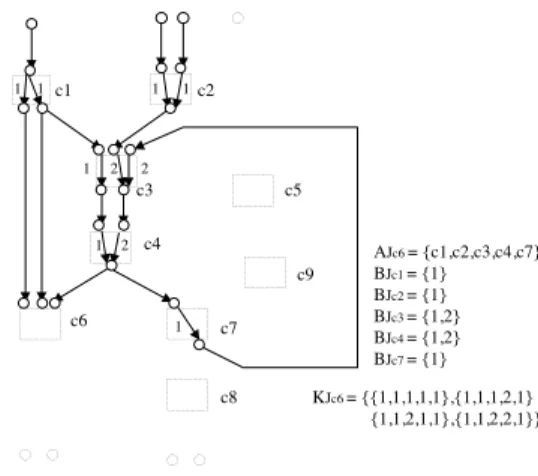
AJc6 = {c1,c2,c3,c4,c7} BJc1 = {1} BJc2 = {1} BJc3 = {1,2} BJc4 = {1,2} BJc7 = {1} KJc6 = {{1,1,1,1,1},{1,1,1,2,1} {1,1,2,1,1},{1,1,2,2,1}}
Figure 9. Control Initial GraphGJc6
of stage 1. However procedures for the other stages can be presented in a similar fashion.
5.2.1 DFT for Consecutive Controllability of Cores (Stage 1)
The objective of the first stage is to modify a given SoC with minimum hardware overhead so that all cores are consecutively controllable for the required TPS (i.e., each core c Chas a justification subgraph GJof c where GJ
satisfies the condition 1 of Theorem 1). The strategy of the algorithm is that, for each core, first it creates control initial graph, and second it creates control middle graph. Then it induces conditions such that the control middle graph satisfies the Definition 6 and the core is consecutively controllable for the required TPS. Then it formalizes the DFT as integer programming problem. All cores are made consecutively controllable with minimum hardware overhead by solving the integer programming problem. Step 1: Creation of Control Initial Graph
The control initial graph GJcof a core c Cis created from a core connectivity graph G as follows.
1. Remove the edges which have labels of c and let the vertices which correspond to the input ports of c be sinks.
2. Remove the edges which have labels of neither JA nor JO.
3. We define the control initial graph GJc as the set of vertices and edges reachable to sinks.
Figure 9 illustrates a control initial graph GJc6. Each edge in GJc6 has a label of either JO or JA and the num- ber beside e Ecorerepresents a label of configuration ID.
Let AJcbe the set of cores that exist in GJc. Here, a core c Cthat exists in GJc means that there exists more than
c1
c2
c3
c4
c6 c7
k1= {1,1,1,1,1} = {v2} JA
JO JA
JA
JA JO JO
JO JO v2
J c6, k1
Q
Figure 10. Control Middle GraphGJc6 k1
one edge which has a label of c in GJc. For each a AJc, let BJa be the set of all configuration IDs of a. We define KJc
as the following equation.
KJc
∏
a AJc
BJa
BJa1 BJa2 BJa3
A control initial graph GJc contains several configurations for each core a AJc, and consecutive transparency of each core a AJcis not realized.
Step 2: Creation of Control Middle Graph
For each k KJc, the control middle graph GJc k is cre- ated from a control initial graph GJcas follows.
1. For each a AJc, select a configuration that corre- sponds to k.
2. We define the control middle graph GJc kas the set of vertices and edges reachable to sinks.
Figure 10 illustrates a control middle graph GJc6 k1. JO and JA beside e Erepresent types of consecutively trans- parent path e. A control middle graph GJc k contains only one configuration for each core a AJc, and consecutive transparency of each core a AJcis realized.
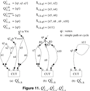
For GJc k, let Q1J
c k, Q 2
Jc k and Q3Jc k be the sets of all ver- tices q GJc kthat satisfies the following conditions respec- tively (Figure 11).
1. Q1J
c k: q is a source. 2. Q2J
c k : q has more than two output edges which have labels of JO.
3. Q3J
c k: There exist cycles which contain q. We define QJc kas follows.
QJc k Q1Jc k Q2Jc k Q3Jc k
CUT (a)
q3in VPI
q2 in Vsource
QJ1 c,k
q1
QJ1,PI c,k = {q3} QJ1,source c,k = {q2} QJ1 c,k = {q1, q2, q3}
s1 s2
S c,k,q1= {s1, s2}
CUT (b) q4
QJ2 c,k
JO JO
JO s3
s4
s9 s10
CUT (b) q5
QJ3 c,k QJ2 c,k = {q4}
QJ3 c,k = {q5}
s11
s6 s7
qi : vertex
si : simple path or cycle
s8 s5
S c,k,q2= {s3, s4} S c,k,q3= {s5, s6} S c,k,q4= {s7, s8 , s9 , s10} S c,k,q5= {s11}
Figure 11.Q1J
c k Q 2 Jc k Q3Jc k
Q2J
c kand Q 3
Jc k are the sets of all vertices that do not satisfy the Definition 6. Moreover, we define Q1 PIJ
c k and Q 1 source Jc k as
follows. Q1 PIJ
c k Q
1
Jc k VPI Q1 sourceJ
c k Q
1
Jc k Vsource
Then, let Sc k qbe the set of all simple paths from q in QJc k
to each sink vertex in GJc k.
Step 3: Integer Programming Formulation
We define the following variables as integer program- ming variables.
yc 1 core c is consecutively controllable for TPS 0 otherwise
ac k
1 GJc kis consecutively controllable for TPS 0 otherwise
dc k q
1 GJc kis consecutively controllable for vertex q
0 otherwise
zq r
1 output edge r of vertex q is consecutively controllable for q
0 otherwise
ms 1 if MUX is inserted to simple path s 0 otherwise
xe 1 if MUX is inserted to interconnect e 0 otherwise
The following integer programming formulation min- imizes the test overhead (i.e., total bit width of MUXs)
while making all cores consecutively controllable. Minimize
∑
ei EN
xei width ei (1)
Subject to:
1. for each core c C,
yc 1 (2)
2. For each core c Cwhich can be tested by either So f f
or Son,
∑
k KJc
ac k yc (3)
3. For each element k KJc,
∑
q QJc k
dc k q QJc k ac k (4)
QJc k is a constant value which represents the number of elements in QJc k.
4. (a) In case TPS type required to test c is So f f for each vertex q Q1J
c k Q
1 PI Jc k ,
∑
s Sc k q
ms Sc k q dc k q (5)
(b) In case TPS type required to test c is Son, for each vertex q Q1J
c k Q
1 PI Jc k Q
1 source
Jc k ,
∑
s Sc k q
ms Sc k q dc k q (6)
5. For each vertex q Q2J
c k, let Rc k q be the set of all output edges of q. For each element r Rc k q, let Src k q be the set of all simple paths between r and all sink vertices in GJc k. Then, for each vertex q Q2J
c k,
∑
r Rc k q
zq r dc k q (7)
∑
s Sc k q Src k q
ms Sc k q Src k q zq r (8)
6. For each vertex q Q3J
c k,
∑
s Sc k q
ms Sc k q dc k q (9)
7. For each simple path s Sc k q,
∑
e Es
xe ms (10)
Esrepresents the set of all edges which correspond to interconnects in simple path s.
Equation (2) guarantees that all cores are consecutively controllable for the required TPS. If TPS type required to test a core is either So f f or Son, more than one GJc k must be consecutively controllable for the TPS. This is guaran- teed by equation (3). In order to make GJc k consecutively controllable for the TPS, all vertices in QJc k must be con- secutively controllable for the TPS. This is guaranteed by equation (4). In order to make q in Q1J
c kconsecutively con- trollable for the TPS, all simple paths in Sc k qmust be in- serted MUXs and paths from TPS must be added. However, if q is a vertex that represents the TPS required to test the core, q is already consecutively controllable for the TPS. This is guaranteed by equation (5) and (6). Each vertex q in Q2J
c khas more than two output edges which have label of JO, and all the edges propagate only the same sequence. In order to make q in Q2J
c k consecutively controllable for the TPS, each edges of q must propagate any test sequence at the same time. This is guaranteed by equation (7) and (8). In order to make q in Q3J
c kconsecutively controllable for the TPS, all cycles which contain q must be broken by MUXs and paths from TPS must be added. This is guaranteed by equation (9). Equation (10) and guarantees that, let s be a simple path and let Esbe the set of all edges which repre- sent interconnects, insertion of MUX to s means that MUX is inserted to more than one element in Es.
Test MUXs are inserted to the edges obtained by solv- ing the above integer programming problem (Figure 12), and all cores can be made consecutively controllable with minimum hardware overhead. However, in case TPS type required to test core c is So f f, it is necessary to add TPSs of type So f f (i.e., add vertices to VPI) if the sum bit width of edges that must be inserted MUXs to make c con- secutive controllable is larger than that of available TPSs (i.e.,vertices in VPI Q1 PIJ
c k). Similarly, in case TPS type re- quired to test core c is Son, it is necessary to add TPSs of type Son(i.e., add vertices to Vsource) if the same condition as above is satisfied.
Procedures for the other stages can be presented in a sim- ilar fashion.
6 Conclusions
In the paper, we introduced a new testability called con- secutive testability. For a consecutively testable SoC, test- ing can be performed as follows. Test patterns of a core are propagated to all input ports of the core from TPS, and
c1
c3
c6 c4 v2 ei
c1
c3
c6 c4 v2 ei
TPS
Figure 12. Insertion of a MUX to an edge ei for Consecutive Controllability
the test responses appeared at an output port of the core are propagated to TRS consecutively at speed of system clock. The propagation of test patterns and responses is achieved by using interconnect and consecutive transparencies of sur- rounding cores. All interconnects can be tested in a similar fashion. Therefore, it is possible to test not only logic faults such as stuck-at faults but also timing faults such as delay faults that require consecutive application of test patterns at speed of system clock. We also proposed a design-for- testability method for making a given SoC consecutively testable based on integer programming problem. Our future work is to propose a DFT method for making cores consec- utively transparent with minimum hardware overhead. Acknowledgments
This work was sponsored in part by NEDO (New En- ergy and Industrial Technology Development Organization) through the contract with STARC (Semiconductor Technol- ogy Academic Research Center) and supported in part by Foundation of Nara Institute of Science and Technology under the Grant for Activity of Education and Research. Authors would like to thank Toshimitsu Masuzawa (Osaka University), Michiko Inoue and Satoshi Ohtake (Nara Insti- tute of Science and Technology) for their valuable discus- sion.
References
[1] Y.Zorian, E.J.Marinissen and S.Dey, ”Testing embedded-core based system chips,” Proc. 1998 Int. Test Conf., pp.130-143, Oct. 1998.
[2] S.Bhatia, T.Gheewala and P.Varma, ”A unifying methodology for intellectual property and custom logic testing,” Proc. 1996 Int. Test Conf., pp.639-648, Oct. 1996.
[3] T.Ono, K.Wakui, H.Hikima, Y.Nakamura and M.Yoshida, ”Integrated and automated design-for-
testability implementation for cell-based ICs,” Proc. 6th Asian Test Symp., pp.122-125, Nov. 1997. [4] P.Varma and S.Bhatia, ”A structured test re-use
methodology for core-based system chips,” Proc. 1996 Int. Test Conf., pp.294-302, Oct. 1998.
[5] N.A.Touba and B.Pouya, ”Testing embedded cores using partial isolation rings,” Proc. 15th VLSI Test Symp., pp.10-16, May 1997.
[6] L.Whetsel, ”An IEEE 1149.1 based test access archi- tecture for ICs with embedded cores, ” Proc. 1997 Int. Test Conf., pp.69-78, Nov. 1997.
[7] M.Nourani and C.A.Papachristou, ”Structural fault testing of embedded cores using pipelining,” Jour- nal of Electronic Testing:Theory and Applications 15, pp.129-144 1999.
[8] I.Ghosh, N.K.Jha and S.Dey, ”A low overhead de- sign for testability and test generation technique for core-based systems-on-a-chip,” IEEE Trans. on CAD, vol.18, no.11, pp.1661-1676, Nov. 1999.
[9] I.Ghosh, S.Dey, and N.K.Jha, ” A fast and low cost testing technique for core-based system-chips,” IEEE Trans. on CAD, vol.19, no.8, pp.863-877, Aug. 2000. [10] S.Ravi, G.Lakshminarayana, and N.K.Jha, ” Testing of Core-Based Systems-on-a-Chip,” IEEE Trans. on CAD, vol.20, no.3, pp.426-439, Mar. 2001.
[11] T.Yoneda and H.Fujiwara, ”A DFT method for core- based systems-on-a-chip based on consecutive testa- bility,” Proc. 10th Asian Test Symp., Nov. 2001(to ap- pear).