Electrical Behavior of GOS Faults in Domino Logic
M. Comte1 S. Ohtake1 H. Fujiwara1 M. Renovell21 Graduate School of Information Science, Nara Institute of Science and Technology (NAIST), Japan Email: {comte, ohtake, fujiwara}@is.naist.jp
2 Laboratoire d’Informatique, de Robotique et de Microélectronique de Montpellier (LIRMM), France Email: [email protected]
Keywords: Domino logic; Gate-Oxide Short (GOS); Defect modeling; Electrical analysis; Boolean test.
Abstract: Gate-Oxide Shorts (GOS) have an increasing impact on the integrated circuit production yield due to the reduction of the related dimensions. The detection of GOS is a challenging issue in the field of testing. This paper presents a detailed study of the impact of a GOS fault affecting a Domino logic circuit. Indeed, Domino logic specific clocked operating principle induces a different behavior from standard full CMOS cells under the effect of a GOS, which can enable GOS detection. Finally, some clues to enhance GOS detection in Domino cells are proposed.
I. Introduction
Testing is a key factor to guarantying Integrated Circuits (IC) proper operation. It should ensure the correct function of the device as well as the targeted performances in terms of delay and current consumption. In order to detect the potential failures of the IC, it is necessary to study the behavior of the circuit affected by a defect, and define a subsequent model of the defect impact. Finally, a test procedure can be proposed from the defined fault model. The defect influence on an IC may depend on the IC nature. In particular, the behavior of Domino logic cells and standard full CMOS cells affected by a similar defect can be different. It is thus necessary to find out a dedicated fault model for each type of IC. In this paper, we present an electrical study of a Domino logic cell affected by a Gate-Oxide Short (GOS) and investigate the achievable detection.
Unlike standard full CMOS gates, Domino gates [1] are implemented with only one type of function (NMOS or PMOS), which is inserted between a precharge PMOS and an evaluation NMOS (see Fig. 1: NMOS function). Precharge and evaluation transistors are connected to a clock signal φ, leading the operation of the Domino gate as a succession of precharge and evaluation phases. In order to enable cascading of gates, the dynamic node is connected to a static inverter (allowing only non-inverting functions). The operation principle of Domino logic gates is developed in section II.
Open defects in Domino logic cells have been studied and some detection methods have been proposed [2, 3]. Resistive short influence on Domino cells and detection through Very Low Voltage (VLV) testing have been presented in [4]. However, [4] deals with gate-to-drain and gate-to- source shorts, but gate-to-channel shorts are not
considered. GOS and more precisely gate-to- channel shorts are the focus of the present paper.
The effects of a GOS on the behavior of a MOS transistor have been studied in detail, and some models have been proposed [5, 6, 7]. The impact of GOS at the transistor level (voltage level and delay degradations, quiescent current), is presented in III.
A detailed analysis of the behavior of a full CMOS logic gate affected by a GOS and possible detection have recently been proposed [10, 11]. Nevertheless, the results cannot be transferred to Domino logic. Section IV shows the detailed study of the behavior of a GOS-affected Domino cell. Finally, section V gives some concluding remarks.
N function VDD
VGND Inputs
Precharge PMOS Clock φ
Evaluation NMOS Output Dynamic node
Static inverter N function
VDD
VGND Inputs
Precharge PMOS Clock φ
Evaluation NMOS Output Dynamic node
Static inverter
Figure 1: Domino logic gate (N type) II. Domino Logic Cell
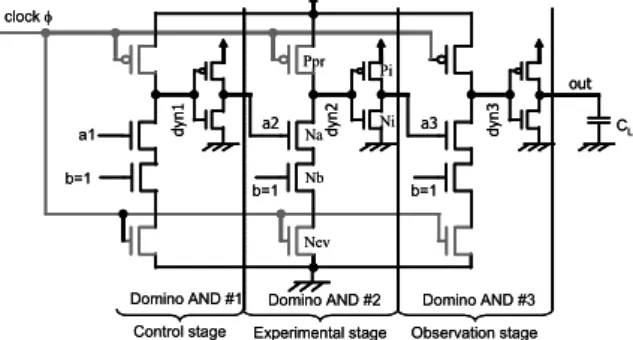
In order to investigate the impact of a GOS on the behavior of a Domino cell, we consider the elementary circuit given in Fig. 2: a chain of three Domino AND gates. Indeed, this structure involves few transistors per gate, so the exhaustive electrical study is achievable.
a1 clock φ
CL
b=1 b=1
b=1
dyn1
a2 dyn2
a3 dyn3 out Na
Nb
Nev
Ppr Pi
Ni
Domino AND #1 Domino AND #2 Domino AND #3 Control stage Experimental stage Observation stage a1
clock φ
CL
b=1 b=1
b=1
dyn1
a2 dyn2
a3 dyn3 out Na
Nb
Nev
Ppr Pi
Ni
Domino AND #1 Domino AND #2 Domino AND #3 Control stage Experimental stage Observation stage
Figure 2: Domino logic structure of study The first Domino AND cell has a role of control stage. It should be considered as a buffer for the following cell that constitutes the experimental stage, in which the GOS will be injected. Finally, the third cell stands as an observation stage. This last cell shows whether the local degradations of the voltage levels, induced by the defect, will spread downstream and result in a faulty behavior of the structure at the primary output (named out). The primary inputs are a1 and b. The load capacitance CL has been designed to be equivalent to one cell input capacitance. The clock signal φ is buffered by
8th IEEE Workshop on Design and Diagnostics of Electronic Circuits and Systems, pp.210-215, April 2005.
a small sized static inverter. The structure has been designed in 0.18µm technology (model card from STMicroelectronics, VDD=1.8V, Vth=0.565V).
Each Domino AND cell is composed of 6 transistors: two signal NMOS (named Na and Nb in the central gate), a precharge PMOS (Ppr), an evaluation NMOS (Nev), and two complementary transistors forming a static inverter (Ni and Pi). The length of the channel is the same for every transistor, and the width ratios are standard for Domino logic (Ni=1, Pi=4, Ppr=2, Na=Nb=Nev=6). All the transistors that are not part of the static inverter constitute a dynamic NAND gate (Ppr, Na, Nb and Nev). The association of a dynamic gate with a static inverter results in a Domino cell. The node between the dynamic gate and the static inverter is usually called the dynamic node. Dynamic nodes of the 1st, 2nd and 3rd Domino cells are called dyn1, dyn2 and dyn3 respectively. Similarly, the first signal inputs of the gates are respectively indicated by a1, a2 and a3, a2 being also the output of the 1st Domino cell and a3 corresponding to the output of the central AND gate. The second signal input, named b, is common to all the cells, and is fixed to the high voltage level. Consequently, the result of the AND functions is led by the value of the first signal input a1.
Figure 3: Timing diagrams of the fault-free circuit In the case of a fault-free structure, the circuit of study operates as shown on the time diagram of Fig 3 (simulation at nominal operating frequency: 10MHz). When φ=0 (precharge phase), the precharge PMOS are active whereas the evaluation NMOS are locked. Therefore, whatever the primary input a1, all dynamic nodes are charged to the high level. Thanks to the static inverters, all gate outputs (a2, a3 and out) are set to the low level. When φ=1, the evaluation phase begins: the precharge PMOS are locked while the evaluation NMOS are active. As a2 and a3 are at the low level, gates #2 and #3 are locked at first. If the primary input a1 is at the low level (left half of the diagram), the first gate is also locked and the circuit state remains the same as previously. Indeed, dyn1 cannot be discharged, so a2 stays at the low level and gate #2 remains locked, and so on. The small overshoot on the dynamic nodes, due to capacitive couplings, is
irrelevant in the operation. On the contrary, if a1=1 (right half), dyn1 is discharged through the active NMOS of the dynamic gate, inducing a switch of a2 to the high level. Consequently, the second Domino cell evaluates its function, discharges its dynamic node, and so forth, like a falling row of dominos. All nodes then switch during evaluation, and switch back at precharge.
It should be pointed out that complex Domino architectures often include in addition keepers and internal prechargers to improve the structure robustness. Nevertheless, they have a significant impact on the circuit performances, so we have not taken them into account yet. Such devices will be added in further work.
III. GOS in standard CMOS
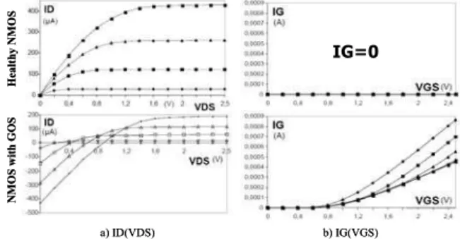
Gate-Oxide Shorts are failures of the isolation in the oxide layer resulting in a resistive path between the gate and bulk of MOS transistors. Consequently, a short current can flow through this path (Fig. 4). The classical equations ruling the operation of a fault-free MOS being based on the oxide layer isolation, they should therefore not be considered in case of GOS-affected transistor.
Gate (PolySi)
oxide (SiO2)
Source Drain
Bulk (Si) IG Gate (PolySi)
oxide (SiO2)
Source Drain
Bulk (Si) IG
Figure 4: Side view of a MOS affected by a GOS The behavior of a MOS transistor affected by an oxide isolation failure has been widely investigated previously [5-9]. The impact of a GOS on the MOS operation induces a modification of the transistor characteristics. The typical alteration of the drain current ID and gate current IG characteristics are illustrated in Fig. 5a and 5b respectively in case of a NMOS. One should note that the defect has no impact when the transistor is off.
IG=0
a) ID(VDS) b) IG(VGS)
Healthy NMOSNMOS with GOS
IG=0
a) ID(VDS) b) IG(VGS)
Healthy NMOSNMOS with GOS
Figure 5: Drain (a) and Gate (b) current characteristics of fault-free (top) and GOS-affected (bottom) NMOS
The classical models of defective transistors affected by a GOS are based on the division of the transistor into an array of smaller transistors. A resistance connecting the common gate to one of the array nodes represents the defect. We consider in this study the lumped MOS transistor model proposed in [8] (which was proposed many years ago and seems questionable for technologies below 90nm, but remains valid here for the considered
0.18µm technology). To implement the lumped MOS model, we replace each transistor of the central cell by an equivalent array of 5 by 6 elementary transistors (5 along the channel width and 6 along the length). The Domino architecture has previously been properly sized so that no elementary MOS gate length is less than 0.18µm.
All transistors in the array have a common bulk and are connected to the same gate G. Transistors at both ends of the array are connected to the same electrodes, forming respectively the global source S and drain D. The GOS defect is injected by connecting a resistance (of any desired value) between the gate and one node in the array (Fig. 6). Position and size of the defect are easily adjusted by moving the connection node in the array and by connecting together several neighboring nodes. Therefore, every unpredictable parameter of the GOS defect is taken into account in the model.
Figure 6: Scheme of the lumped MOS model IV. GOS in dynamic CMOS
We have studied the behavior of the Domino logic structure of study (Fig. 2) for GOS affecting each transistor of the central cell. We assume single fault, i.e. we inject one GOS at once. The GOS defect is thus successively injected into Na, Nev, Ppr, Pi and Ni. For each case, the unpredictable parameters of the defect have been considered. 1. GOS in the signal transistor
We inject a GOS defect is the NMOS signal transistor Na. In a first place, we consider a small GOS defect of size one node, located in the center of the array, with a very low resistance of 1Ω.
As mentioned in III, the effect of the GOS on the behavior of Na (and consequently on the behavior of the cell) should be observed when Na is on (a2=1). It implies that a1=1. In addition, the observation should be made during evaluation. Indeed, Nev is then on, which enables the short current Ishort to flow from the PMOS of the upstream static inverter through the defective gate of Na to the ground (see Fig. 7).
The time diagrams of the voltage levels involved in the signal path of the Domino structure are illustrated in Fig. 8 at nominal frequency (10MHz). As expected, the injected GOS has no impact on the Domino cell behavior during precharge phase or when a1=0. On the contrary, some degradations of the voltage levels of nodes a2 and dyn2 can be observed during evaluation when a1=1. These two nodes are respectively located directly upstream and downstream of the affected transistor. The node
a2, corresponding to the faulty transistor gate, reaches only 63% of its nominal voltage. The dynamic node dyn2, connected to the drain of Na, which should be at the low level in this configuration, reaches 26% of the voltage range. Although the voltage alterations are severe, they are not sufficient to induce a false logic state, so the defect is not detectable via a Boolean test.
a1 clock φ
CL
b=1 b=1
b=1
dyn1
a2
dyn2
a3
dyn3
out
Na* Nb
Nev
Ppr Pi
Ni
Ishort a1
clock φ
CL
b=1 b=1
b=1
dyn1
a2
dyn2
a3
dyn3
out
Na* Nb
Nev
Ppr Pi
Ni
Ishort
Figure 7: Conductive path of Ishort (GOS in Na)
0 0.5 1 1.5 2
0 0.5 1 1.5 2 2.5
0 0.5 1 1.5 2 2.5
0.00E+00 5.00E-08 1.00E-07 1.50E-07 2.00E-07 2.50E-07 3.00E-07
clock a1
dyn1 dyn2 dyn3
a2 a3 out
Clock & a1 (V)Dynamic nodes (V)Outputs (V)
- -
Time (s) Time (s) Time (s) 0
0.5 1 1.5 2
0 0.5 1 1.5 2 2.5
0 0.5 1 1.5 2 2.5
0.00E+00 5.00E-08 1.00E-07 1.50E-07 2.00E-07 2.50E-07 3.00E-07
clock a1
dyn1 dyn2 dyn3
a2 a3 out
Clock & a1 (V)Dynamic nodes (V)Outputs (V)
- -
Time (s) Time (s) Time (s)
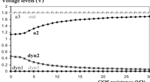
Figure 8: Time diagrams of the voltage levels, GOS in Na (1 node centered, 1Ω, 10MHz) We now consider the unpredictable parameters of the GOS defect injected in Na. In a first place, we investigate the influence of the GOS resistance. The values of all the voltage levels obtained when the defect is activated are presented in Fig. 9 for GOS resistance varying from 0 to 30kΩ. The defect size is still 1 node, located in the center of the model array, and the operation frequency is nominal (10MHz). Simulations show that the nodes a2 and dyn2 exhibit the only voltage levels that are significantly affected by the defect. When the resistance of the defect increases, the value of these node voltage levels get closer to their nominal values. Whatever the resistance, the presence of the GOS defect never induces a false logic state. Therefore it cannot be detected via Boolean test.
0 0.2 0.4 0.6 0.8 1 1.2 1.4 1.6 1.8 2
0 5 10 15 20 25 30
GOS resistance (kΩ) dyn1
dyn2 dyn3 a2 a3 out Voltage levels (V)
0 0.2 0.4 0.6 0.8 1 1.2 1.4 1.6 1.8 2
0 5 10 15 20 25 30
GOS resistance (kΩ) dyn1
dyn2 dyn3 a2 a3 out Voltage levels (V)
Figure 9: Influence of the GOS resistance
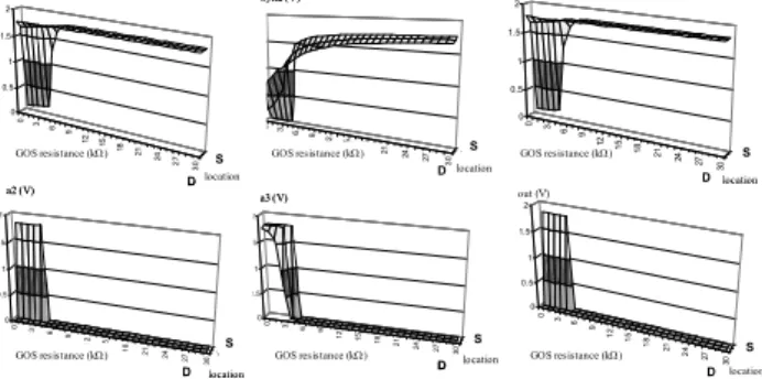
The GOS position along the gate has a weak influence in this case. Fig. 10 presents the evolution of the voltage levels of nodes a2 (a) and dyn2 (b) along the value of the GOS resistance (ranging from 0 to 30kΩ) for the five locations along the gate. The simulation conditions are the same as previously. Concerning the position, "D" indicates a location of the defect very close to the drain, while
"S" corresponds to a position neighboring the source of the faulty transistor.
0 9
18 27
1 3 5
0 0. 2 0. 4 0. 6 0.8 1 1.2 1.4 1.6 1.8
0 8 16
24
1 2 3 45 0 0. 2 0.4 0.6 0.8 1 1. 2 1.4 1.6 1.8
a) a2 voltage level b) dyn2 voltage level dyn2 (V)
a2 (V)
GOS resistance (kΩ) GOS resistance (kΩ)
location location
D
S
D
S 0
9 18
27
1 3 5
0 0. 2 0. 4 0. 6 0.8 1 1.2 1.4 1.6 1.8
0 8 16
24
1 2 3 45 0 0. 2 0.4 0.6 0.8 1 1. 2 1.4 1.6 1.8
a) a2 voltage level b) dyn2 voltage level dyn2 (V)
a2 (V)
GOS resistance (kΩ) GOS resistance (kΩ)
location location
D
S
D
S
Figure 10: Influence of the GOS position on voltage levels a2 (a) and dyn2 (b) We can observe that the GOS impact on the level of a2 (gate of the affected MOS) is more significant when the defect is located close to the source. In this case, a2 reaches only 58% of its nominal voltage level. On the contrary, the voltage level of dyn2 is more affected when the GOS is closer to the drain (up to 30% of VDD). These observations match the results obtained in the context of standard CMOS cells [10]. Nevertheless, the defect cannot be detected via Boolean test.
0 4 8 12 16 20 24 28 1
0 0.5 1 1.5 2
0 3 6 9 12 15 18 21 24 27 30
1 0
0.5 1 1.5 2
0 4 8 12 16 20 24 28 1
0 0.5 1 1.5 2
0 4 8 12 16 20 24 28 1
0 0.5 1 1.5 2
0 4 8 12 16 20 24 28 1
0 0.5 1 1.5 2
Rgos (kohms)
0 3 6 9 12 15 18 21 24 27 30
1 0
0.5 1 1.5 2
Rgos (kohm s) D
S
D D
D dyn2 (V)
GOS resistance (kΩ)
location GOS resis tance (kΩ)
GOS resis tance (kΩ) GOS resistance (kΩ) GOS resistance (kΩ)
GOS resistance (kΩ)
location location
location location
location
dyn1 (V) dyn3 (V)
a2 (V)
D
a3 (V) out (V)
D
S S
S S S
0 4 8 12 16 20 24 28 1
0 0.5 1 1.5 2
0 3 6 9 12 15 18 21 24 27 30
1 0
0.5 1 1.5 2
0 4 8 12 16 20 24 28 1
0 0.5 1 1.5 2
0 4 8 12 16 20 24 28 1
0 0.5 1 1.5 2
0 4 8 12 16 20 24 28 1
0 0.5 1 1.5 2
Rgos (kohms)
0 3 6 9 12 15 18 21 24 27 30
1 0
0.5 1 1.5 2
Rgos (kohm s) D
S
D D
D dyn2 (V)
GOS resistance (kΩ)
location GOS resis tance (kΩ)
GOS resis tance (kΩ) GOS resistance (kΩ) GOS resistance (kΩ)
GOS resistance (kΩ)
location location
location location
location
dyn1 (V) dyn3 (V)
a2 (V)
D
a3 (V) out (V)
D
S S
S S S
Figure 11: Voltage levels (9-node GOS in Na) Finally, we consider defect sizes of 9 and 21 nodes in the array. The impact of a 9-node GOS on the voltage levels of all nodes along the resistance and the three positions along the channel are presented in Fig. 11. When the resistance of the defect is very low (≤1kΩ) and the defect is closer to the source, a false logic state is observed on all nodes downstream the defective MOS (dyn2, a3, dyn3 and out). Then, Boolean detection of the GOS is possible on the primary output. We obtain similar results for a 21-node defect (results not shown).
To summarize, a GOS defect in the signal transistor of a Domino cell can be detected via Boolean test when the short resistance is inferior to 1kΩ, the defect size is at least 40% of the gate surface and the defect is not close to the drain.
2. GOS in the evaluation transistor
We now investigate the effect of a GOS affecting the evaluation NMOS Nev of the central cell. In this case, the gate of the faulty transistor is connected to the clock signal φ, so the defect is activated during every evaluation phase (φ=1). In this configuration, the short current flows from the power supply via the PMOS transistor of the clock buffer, through the faulty gate of Nev, to the ground. The voltage levels of φ as well as the internal node between Nev and Nb are affected. As we assume b=1, Nb is on and consequently the voltage level of the internal node between Nb and Na is also influenced. Whatever the unpredictable parameters, the voltage levels of the nodes upstream from the faulty transistor (dyn1 and a2) are not affected.
In case a1 is at the low level, and consequently so is a2, the signal transistor Na is off. Therefore, the GOS effect is not spread downstream. It should be noted that the small overshoots on the dynamic nodes mentioned in II are partially discharged toward the nominal high voltage level. Indeed, the level of φ is affected, therefore the precharge PMOS compensates for the capacitive couplings. Whatever the unpredictable parameters, no GOS impact is noticeable on the signal voltage levels.
In case a1=1, dyn2 is not fully discharged after the precharge phase as far as Nev is defective. The behavior of the Domino structure is very similar to the one observed when the GOS affects the signal transistor Na (except that the node a2 is not affected). Thus, results are not shown here. The same conclusions as in section IV.1 can be derived. 3. GOS in the precharge transistor
Symmetrically, we study the impact of a GOS located in the precharge PMOS Ppr of the central gate. Under this condition, the defect is active during precharge (φ=0). The nominal level of the dynamic nodes is then high. The short current flows through Ppr defective gate to the ground via the NMOS of the clock buffer. The defect influence upon the voltage levels downstream depends on a1.
When a1=0, Na is off. The voltage level of dyn2 is directly affected by the leakage through Ppr. But whatever the unpredictable parameters, the degradation of the voltage level of dyn2 is never severe enough to have an impact on the nodes downstream. Indeed, the minimal value of dyn2 (9- node GOS close to the drain) is still 58% of its nominal value. A GOS affecting the precharge transistor could therefore not be detected by Boolean test under these conditions.
When a1=1, Na is on. As we assume b=1, Nb is also on. Moreover, the defect impact upon the voltage level of φ prevents Nev from being completely off. As a result, a conductive path between VDD and the ground through the dynamic gate appears. Consequently, the degradation of dyn2 voltage level is more severe than previously.
In addition, the clock level degradation also impacts the control and observation gates. All the dynamic gates in the structure exhibit a short path, resulting in a degradation of all dynamic node levels.
A defect sized 1 node does not induce any of the static inverters to commute. The voltage levels of dyn1 and dyn3 are defined only by the level of φ. The clock signal is connected to the gate of the defective PMOS, so the worst deviation should be obtained when the defect is close to the source. Indeed, we obtain the minimal value of dyn1 and dyn3 (87% of the nominal value) in this case. On the contrary, dyn2 is directly influenced as the drain of the faulty transistor. The minimal value of dyn2 (66% of the nominal precharge level), appears when the defect is close to the drain.
Bigger sized GOS can induce Boolean errors as shown in Fig. 12 in case of a 9-node defect. If the test is achieved on the primary output, the defect can be detected if it is located close to the source and its resistance is inferior to 5kΩ. The internal nodes dyn1, a2 and dyn3 exhibit the same sensitivity to the GOS impact. The closest nodes downstream the defect, dyn2 and a3, are more affected (wrong state observed for RGOS≤4kΩ). Similar results are observed for a 21-node defect.
0 3 6 9 12 15 18 21 24 27 30
1 0
0.5 1 1.5 2
0 3 6 9 12 15 18 21 24 27 30
1 0
0.5 1 1.5 2
0 3 6 9 12 15 18 21 24 27 30
1 0
0.5 1 1.5 2
0 3 6 9 12 15 18 21 24 27 30
1 0
0.5 1 1.5 2
0 3 6 9 12 15 18 21 24 27 30
1 0
0.5 1 1.5 2
0 3 6 9 12 15 18 21 24 27 30
1 0
0.5 1 1.5 2
D S
D D
D dyn2 (V)
GOS resistance (kΩ)
location GOS resistance (kΩ)
GOS resistance (kΩ) GOS resistance (kΩ) GOS resistance (kΩ)
GOS resistance (kΩ)
location location
location location
location
dyn1 (V) dyn3 (V)
a2 (V)
D
a3 (V) out (V)
D
S S
S S S
0 3 6 9 12 15 18 21 24 27 30
1 0
0.5 1 1.5 2
0 3 6 9 12 15 18 21 24 27 30
1 0
0.5 1 1.5 2
0 3 6 9 12 15 18 21 24 27 30
1 0
0.5 1 1.5 2
0 3 6 9 12 15 18 21 24 27 30
1 0
0.5 1 1.5 2
0 3 6 9 12 15 18 21 24 27 30
1 0
0.5 1 1.5 2
0 3 6 9 12 15 18 21 24 27 30
1 0
0.5 1 1.5 2
D S
D D
D dyn2 (V)
GOS resistance (kΩ)
location GOS resistance (kΩ)
GOS resistance (kΩ) GOS resistance (kΩ) GOS resistance (kΩ)
GOS resistance (kΩ)
location location
location location
location
dyn1 (V) dyn3 (V)
a2 (V)
D
a3 (V) out (V)
D
S S
S S S
Figure 12: Voltage levels (9-node GOS in Ppr) It should be pointed out that we observe a voltage level degradation on dyn2 during evaluation when a1=0. Indeed, although the defective Ppr should be off (φ=1), the GOS affects the upstream voltage levels. So Ppr is partially on and a voltage drop appears between VDD and dyn2. However, the voltage level never drops below 60% of VDD. Therefore, the alteration is not spread downstream and the defect cannot be detected via Boolean test.
To summarize, a GOS in Ppr can be detected during precharge phase when a1=1. The achievable detection range is restricted to a few kΩ.
4. GOS in the PMOS of the static inverter To activate a GOS affecting the PMOS of the central static inverter Pi, the voltage level at the gate of Pi should be low. In other words, the GOS effects can be observed during evaluation phase when a1=1 in order to discharge dyn2. In this case, the short current flows through the gate of Pi, via Na, Nb and Nev which are all on, to the ground. Consequently, dyn2 is not properly discharged. The
output of the static inverter a3 is more sensitive to the degradation of dyn2 than previously as far as the inverter transfer function is affected by the GOS.
For a 1-node sized defect, the maximal voltage level of dyn2 reaches 34% of the voltage range for a null resistance when the defect is close to the source. The most significant decrease of a3 (to 66% of its nominal value) happens for a null resistance when the defect is close to the drain. The other nodes are not affected. In any case, a 1-node sized defect in Pi is not detectable by a Boolean test.
When the size of the defect is superior, defect resistances lower than 1kΩ lead to a false logic state. The detailed observations are very similar to the ones made in case of a GOS affecting Na. 5. GOS in the NMOS of the static inverter
A GOS in the NMOS Ni of the central inverter is activated when the nominal level of dyn2 (gate of Ni) is high. This condition is fulfilled both during precharge (whatever a1) and during evaluation when a1=0. The behavior of the Domino structure is different depending on the operating phase, so we will consider each case separately.
During precharge phase, the short current flows from the power supply, via Ppr, through the defective gate of Ni, to the ground. The voltage levels of dyn2 and a3, connected respectively to the gate and drain of Ni, are significantly affected. A GOS sized 9 nodes or more induces a false logic state of a3 if its resistance is inferior to 5kΩ whatever its location along the gate. Nevertheless, the defect has no impact at all upon the voltage levels of the nodes downstream during precharge, as far as the precharge of node dyn3 neither depends on dyn2 nor on a3.
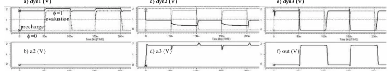
Notwithstanding, the defect can be detected under the same conditions (size≥9 nodes and RGOS≤5kΩ) during evaluation with a1=0. Indeed, the Domino structure behaves as shown in Fig. 13. The dynamic node dyn1 is normally charged during precharge (a), and suffers no leakage during evaluation. Then, a2 stands at the nominal low level during the whole clock cycle (b). On the contrary, dyn2 level of precharge is severely affected by the defect (c). Moreover, the leakage through the defective gate leads to an additional discharge of dyn2. Indeed, during evaluation (φ=1) when a1=a2=0, both Ppr and Na are off, leading to a floating node dyn2. This high impedance state of dyn2 is particularly interesting; Additional details are given hereafter. The degradation of dyn2 level results in a false logic state of a3 whatever the clock phase (d). As mentioned in the previous paragraph, the influence of the false state during precharge has no effect on the following voltage levels. On the contrary, during evaluation, the Boolean error is spread downstream. Indeed, as a3=1, the signal NMOS of the observation cell is on and dyn3 is fully discharged (e). Consequently, out is high (f) while its nominal level is low (a1=0).
φ=1 evaluation precharge
φ=0 a) dyn1 (V)
b) a2 (V)
c) dyn2 (V)
d) a3 (V)
e) dyn3 (V)
f) out (V) φ=1
evaluation precharge
φ=0 a) dyn1 (V)
b) a2 (V)
c) dyn2 (V)
d) a3 (V)
e) dyn3 (V)
f) out (V)
Figure 13: Time diagrams for a GOS in Ni with a1=0 (9-node, close to the drain, null resistance, 10MHz) The discharge of high impedance node dyn2
during evaluation depends on the unpredictable parameters. The discharge time constant decreases with the defect resistance or when the defect size increases. The defect location along the gate is of no significant influence. The voltage level obtained at the end of the evaluation phase has been measured for all nodes varying the unpredictable parameters at nominal frequency 10MHz. Results in case of a 1-node defect are shown in Fig. 14. The voltage levels of nodes dyn1 and a2 are not affected by the defect and are thus not illustrated hereafter. A false Boolean state on out is observed for defect resistances up to 24kΩ. We obtain the same resistance detection range for bigger defects.
0 3 6 9 12 15 18 21 24 27 30 1
0 0.5 1 1.5 2
0 3 6 9 12 15 18 21 24 27 30 1
0 0.5 1 1.5 2
0 4 8 12 16 20 24 28 1
0 0.5 1 1.5 2
0 4 8 12 16 20 24 28 1
0 0.5 1 1.5 2
D D
D dyn2 (V)
GOS resistance (kΩ)
location
GOS resistance (kΩ) GOS resistance (kΩ)
GOS resistance (kΩ)
location
location location
dyn3 (V)
a3 (V) out (V)
D
S S
S S
0 3 6 9 12 15 18 21 24 27 30 1
0 0.5 1 1.5 2
0 3 6 9 12 15 18 21 24 27 30 1
0 0.5 1 1.5 2
0 4 8 12 16 20 24 28 1
0 0.5 1 1.5 2
0 4 8 12 16 20 24 28 1
0 0.5 1 1.5 2
D D
D dyn2 (V)
GOS resistance (kΩ)
location
GOS resistance (kΩ) GOS resistance (kΩ)
GOS resistance (kΩ)
location
location location
dyn3 (V)
a3 (V) out (V)
D
S S
S S
Figure 14: Voltage levels (1-node GOS in Ni) When the defect is more resistive, the discharge time constant prevents the voltage level from reaching a false logic state during evaluation. In a test view, we can then consider decreasing the frequency in order to enlarge the resistance detection range. Indeed, with a reduced frequency, the evaluation phase becomes longer and the charge transfer has more chances to be fully achieved. We perform the same measures as previously with a frequency 10 times lower (1MHz). Indeed, the resistance detection is extended up to 7MΩ for a defect as small as 4% of the gate (1 node). We can therefore consider that a GOS located in the NMOS of a static inverter in a Domino cell can be detected via a Boolean test whatever the unpredictable parameters if the test frequency is set to one order of magnitude below the nominal frequency. The adequate ratio of the test and nominal frequencies should be adapted to the Domino circuit under test.
V. Conclusion
We have carried out a detailed electrical study of an elementary Domino logic circuit affected by a
Gate-Oxide Short. We expected beforehand that the clocked operation principle combined to the reduced noise margins of Domino circuits would lead to better possible detection via Boolean test than obtained in standard CMOS cells. Nevertheless, it has been shown in this study that GOS detection remains particularly difficult to achieve. The achievable resistance detection ranges are globally comparable to the ones obtained for standard CMOS. An interesting case, when the defect affects the NMOS of the static inverter, leads to a high impedance state that can be detected whatever the defect parameters.
In future work, GOS detection by quiescent current test (IDDQ) and delay faults will be investigated. In a second step, keepers and internal prechargers will be taken into consideration to obtain a more realistic Domino architecture. Finally, the specific behavior of GOS upon technologies below 90nm will be investigated with a different model.
Acknowledgement: This work was supported in part by 21st Century COE (Center of Excellence) Program "Ubiquitous Networked Media Computing" and in part by JSPS (Japan Society for the Promotion of Science) under Grants-in-Aid for Scientific Research B(2) (No. 15300018).
References:
[1] N. Weste & K. Eshraghian, "Principles of CMOS VLSI Design, A System Perspective", 2nd ed., Addison-Wesley Publications Co., ISBN 0-201-53376-6, 1992.
[2] V.G. Oklobdzija & P.G. Kovijanic, "On Testability of CMOS-Domino Logic", 14th International Conference on Fault-Tolerant Computing, pp. 50-55, 1984.
[3] H. Wunderlich & W. Rosentiel, "On Fault Modeling for Dynamic CMOS Circuits", 23rd Design Automation Conference, pp. 540-546, 1986.
[4] J. T.-Y. Chang & E. J. McCluskey, "Detecting Resistive Shorts for CMOS Domino Circuits", Proc. International Test Conference, pp. 890-899, 1998.
[5] C.F. Hawkins & J.M. Soden, "Electrical Characteristics and Testing Considerations for Gate Oxide Shorts in CMOS ICs", Proc. International Test Conference, pp. 544-555, 1985. [6] M. Syrzyki, "Modeling of Gate Oxide Shorts in MOS
Transistors", Trans. On Computer-Aided Design of Integrated Circuits and Systems, vol. 8, #3, pp. 193-202, March 1989. [7] J. Segura, C. De Benito et al., "A Detailed Analysis and
Electrical Modeling of Gate Oxide Shorts in MOS Transistors", Journal of Electronic Testing: Theory and Application (JETTA), vol.8, #3, pp. 229-239, June 1996. [8] M. Syrzyki, "Modeling of Spot Defects in MOS Transistors",
Proc. International Test Conference, pp. 148-157, 1987. [9] J.M. Soden & C.F. Hawkins, "Test Considerations for Gate
Oxide Shorts in CMOS ICs", IEEE Design and Test of Computers, pp. 56-64, August 1986
[10] M. Renovell, J.M. Gallière et al., "Boolean and Current Detection of MOS Transistor with Gate Oxide Short", International Test Conference, pp. 1039-1048, 2001. [11] M. Renovell, J.M. Gallière et al., "Delay Testing of MOS
Transistor with Gate Oxide Short", 12th Asian Test Symposium, pp. 168-173, 2003.