[Issue No.]
T11-0004
[Page]
1/2
[Title]
Caution when using digital to analog converter module
[Date of Issue]
June, ‘03
[Relevant Models]
Q62DA, Q64DA, Q68DAI
HEAD OFFICE : 1-8-12, OFFICE TOWER Z 14F HARUMI CHUO-KU 104-6212, JAPAN NAGOYA WORKS : 1-14, YADA-MINAMI 5-CHOME, HIGASHI-KU, NAGOYA, JAPAN
T ECH N I CAL BU LLET I N
T ECH N I CAL BU LLET I N
T ECH N I CAL BU LLET I N
T ECH N I CAL BU LLET I N
Thank you for your continued support of Mitsubishi programmable logic controllers, MELSEC-Q series.
When the Q-series digital to analog converter module (Q62DA, Q64DA or Q68DAI) satisfies all of the conditions shown in 1
(1) to (3), the analog output current and the external load resistance value vary within the range given in the performance
specifications list. (If any of (1) to (3) is not satisfied, the following caution is not applied.)
1. Conditions
(1) The current output is used.
(2) The external load resistance value exceeds 480
.
(3) The external power supply voltage is less than 22.85V DC.
2. Caution
The following shows the analog output current and the external load resistance value when the external power supply
voltage is less than 22.85V DC.
Determine the external power supply voltage referring to the graph below.
22.85V to 28.8V
22V
21V
20.4V
20
18.5
17.3
16.5
A
nal
og
out
p
u
t current
(m
A
)
External load resistance value ( )
510
480
550
600
External power supply
Remarks
[Issue No.]
T11-0004
[Page]
2/2
[Title]
Caution when using digital to analog converter module
[Date of Issue]
June, ‘03
[Relevant Models]
Q62DA, Q64DA, Q68DAI
HEAD OFFICE : 1-8-12, OFFICE TOWER Z 14F HARUMI CHUO-KU 104-6212, JAPAN NAGOYA WORKS : 1-14, YADA-MINAMI5, HIGASHI-KU, NAGOYA, JAPAN
T ECH N I CAL BU LLET I N
T ECH N I CAL BU LLET I N
T ECH N I CAL BU LLET I N
T ECH N I CAL BU LLET I N
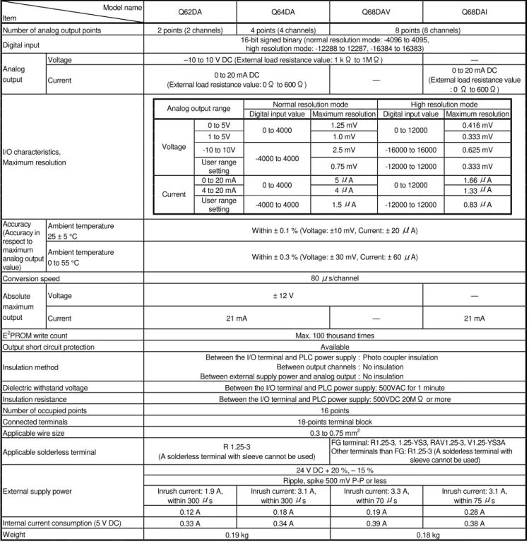
Table 3.1 Performance specifications list (Reference)
Model name
Item Q62DA Q64DA Q68DAV Q68DAI
Number of analog output points 2 points (2 channels) 4 points (4 channels) 8 points (8 channels)
Digital input 16-bit signed binary (normal resolution mode: -4096 to 4095, high resolution mode: -12288 to 12287, -16384 to 16383)
Voltage –10 to 10 V DC (External load resistance value: 1 k to 1M ) —
Analog
output Current 0 to 20 mA DC
(External load resistance value: 0 to 600 ) —
0 to 20 mA DC (External load resistance value
: 0 to 600 )
Normal resolution mode High resolution mode
Analog output range
Digital input value Maximum resolution Digital input value Maximum resolution
0 to 5V 1.25 mV 0.416 mV
1 to 5V 0 to 4000 1.0 mV 0 to 12000 0.333 mV
-10 to 10V 2.5 mV -16000 to 16000 0.625 mV
Voltage
User range setting
-4000 to 4000
0.75 mV -12000 to 12000 0.333 mV
0 to 20 mA 5 A 1.66 A
4 to 20 mA 0 to 4000 4 A 0 to 12000 1.33 A
Current
User range
setting -4000 to 4000 1.5 A -12000 to 12000 0.83 A
I/O characteristics, Maximum resolution
Ambient temperature
25 ± 5 °C Within ± 0.1 % (Voltage: ±10 mV, Current: ± 20 A)
Accuracy (Accuracy in respect to maximum analog output value)
Ambient temperature
0 to 55 °C Within ± 0.3 % (Voltage: ± 30 mV, Current: ± 60 A)
Conversion speed 80 s/channel
Voltage ± 12 V —
Absolute maximum
output Current 21 mA — 21 mA
E2PROM write count Max. 100 thousand times
Output short circuit protection Available
Insulation method
Between the I/O terminal and PLC power supply : Between output channels : Between external supply power and analog output :
Photo coupler insulation No insulation No insulation
Dielectric withstand voltage Between the I/O terminal and PLC power supply: 500VAC for 1 minute
Insulation resistance Between the I/O terminal and PLC power supply: 500VDC 20M or more
Number of occupied points 16 points
Connected terminals 18-points terminal block
Applicable wire size 0.3 to 0.75 mm2
Applicable solderless terminal R 1.25-3
(A solderless terminal with sleeve cannot be used)
FG terminal: R1.25-3, 1.25-YS3, RAV1.25-3, V1.25-YS3A Other terminals than FG: R1.25-3 (A solderless terminal with
sleeve cannot be used) 24 V DC + 20 %, – 15 %
Ripple, spike 500 mV P-P or less Inrush current: 1.9 A,
within 300 s
Inrush current: 3.1 A,
within 300 s
Inrush current: 3.3 A,
within 70 s
Inrush current: 3.1 A,
within 75 s
External supply power
0.12 A 0.18 A 0.19 A 0.28 A
Internal current consumption (5 V DC) 0.33 A 0.34 A 0.39 A 0.38 A