A BIST Method Based on Concurrent Single-Control Testability of RTL Data
Paths
Ken-ichi Yamaguchi Hiroki Wada Toshimitsu Masuzawa
†and Hideo Fujiwara
Graduate School of Information Science, Nara Institute of Science and Technology
8916-5 Takayama, Ikoma, Nara, 630-0101, Japan
[email protected], [email protected],
[email protected], [email protected]
Abstract
This paper presents a new BIST(Built-In Self-Test) method for register transfer level data paths based on both hier- archical testing and “test-per-clock” scheme. In the pro- posed method, test pattern generators and response analyz- ers are placed on primary inputs and primary outputs, and test patterns and test responses are transferred along paths in the data paths. This paper proposes a new testability for BIST, concurrent single-control testability, and presents a new BIST method based on the testability. The concurrent single-control testability is an extension of single-control testability we proposed in [2] and has advantage that test application time becomes shorter because multiple combi- national modules can be tested at the same time (i,e., con- current testing). Our experimental results show that the pro- posed method reduces test application time without increas- ing so much hardware overhead compared with the previous method.
keywords: design for testability, RTL data path, built-in self-test, single-control testability, hierarchical test, concur- rent test
1 Introduction
Built-in self-test (BIST) is one of the most important techniques for testing large and complex VLSI circuits. In this technique, test pattern generators (TPGs) are added to primary inputs (PIs) and response analyzers (RAs) are added to primary outputs. However, adding these TPGs and RAs is not sufficient to achieve high fault coverage, if the VLSI circuit contains cycles in its structure. Thus, several techniques of design for testability (DFT) have been pro- posed [1].
BIST methods are classified into the test-per-scan scheme and the test-per-clock scheme. In the test-per-scan scheme, (some) registers are modified into scan registers so that test patterns and test responses can be shifted into and out using a scan path. A major drawback of this scheme is long test application time caused by the scan. Another major drawback is difficultly in applying test patterns at the operational speed of the circuits (at-speed test). At-speed test is important since it can detect more defective circuits than the same test sequence applied at a lower rate in scan mode.
The author is currently with Central Research Laboratory, Hitachi,Ltd.
†The author is currently with Guraduate School of Engineering Sci- ence, Osaka University
In the test-per-clock scheme, some register are enhanced so that they can generate test patterns and/or compact test responses. Examples of these registers are BILBO(built-in logic block observer)[3] and CBILBO(concurrent BILBO). The advantage of this scheme is that at-speed test is possible and thus test application time is short. However, test-per- clock scheme generally requires higher hardware overhead than the test-per-scan scheme.
Masuzawa et al. [2] proposed single-control testability of register-transfer-level(RTL) data paths as testability suit- able to BIST of the test-per-clock scheme and presented a DFT method based on the testability. This DFT method is based on hierarchical test: each combinational module (i.e., an operational module or a multiplexor) is tested indepen- dently from other modules. The single-control testability guarantees that, for each combinational module, test pat- terns generated by TPGs can be fed into the module at con- secutive system clocks and its test responses can be consec- utively propagated to an RA. In other words, it can realize a configuration equivalent to that where TPGs are placed immediately before the inputs of the module and an RA is placed immediately after the output of the module. Thus, the single-control testability guarantees high fault coverage (for single stuck-at-fault). Moreover, the BIST can also de- tect some faults of other fault models (e.g.,transition faults and delay faults) that require consecutive application of test patterns at speed of system clock. The drawback of the BIST is long test application time, because the BIST tests only a single module at a time.
In this paper, we proposes a new testability, concurrent single-control testability, to remedy the drawback. The pro- posed testability is an extension of the single-control testa- bility and has an advantage that test application time be- comes shorter because multiple combinational modules can be tested at the same time. We also present a DFT method for modifying a data path to a concurrent single-control testable one with low hardware overhead. To guarantee propagation of test patterns and test responses, some opera- tional modules are augmented with thru function and some multiplexors are added. Therfore, this method can guar- antee high fault coverage. Experimental results for some benchmark circuits show that the hardware overhead is not so high.
The advantages of our BIST are summarized as follows. High fault coverage
Low hardware overhead Short test application time IEEE the 10th Asian Test Symposium (ATS 2001), pp. 313-318, Nov. 2001.
PIPI PI
PO PO
PIPI PI
PO PO
(a)a data path (b)a data path digraph Figure 1. A data path and its data path digraph
At-speed testability.
The paper is organized as follows. In Section2, we intro- duce a data path and its graph model. Section3 introduces the concurrent single-control testability. Section4 presents the DFT method for the concurrent single-control testabil- ity. We present experimental results in Section5 and con- clude with Section6.
2 Data Path
A data path consists of hardware elements and lines. A hardware element is a primary input (PI), a primary out- put (PO), a register, a multiplexor (MUX), or an opera- tional module. An operational module is a combinational circuit and includes no register. In the rest of this paper, operational modules and MUXs are simply called (combi- national) modules. We introduce ports as interface points of each hardware element in a natural fashion: values en- ter into a hardware element through its input ports, and exit through its output port. For convenience, we regard a PI (resp. a PO) as an output port (resp. an input port). A line connects an output port with an input port. Any number of lines can connect to an output port (i.e., fanout is allowed), but only one line can connect to an input port.
We use a data path digraph G=(V A) to represent struc- ture of a data path:
V V1 V2where
– V1is the set of all hardware elements in the data path, and
– V2is the set of all ports in the data path. A A1 A2 A3where
– A1 x y V2 V2 output port x is connected to input port y by a line ,
– A2 y u V2 V1 yis an input port of u , – Aand3 u x V1 V2 xis an output port of u . Figure 1 illustrates a data path and its data path digraph. This figure also demonstrates the correspondence between a data path and its data path digraph. The data paths consid- ered in this paper are fairly general and satisfy most of the standard assumptions applicable to data path design. We as- sume, for simplicity, that each module has exactly two input ports and only one output port. We denote the vertex sets V1
and V2 of data path digraph G by G V1 and G V2respec- tively. Similarly, we use notation G A1 G A2and G A3for the edge sets. We denote the vertex set of (combinational) modules by Vc V1 .
For a data path with thru function, we define a data path digraph with thru function G as follows: the data path di- graph with thru function is the digraph obtained from its data path digraph by removing all edges (y u) A2 such that input port y does not have thru function. Thus, any value can be propagated along any path in the data path di- graph with thru-function.
3 Concurrent Single-Control Testability
3.1 Single-Control TestabilityMasuzawa et al.[2] proposed single-control testability of RTL data paths for BIST, and proposed a design for testa- bility (DFT) method that transforms a given data path to a single-control testable one. The single-control testability is defined as follows.
Definition1 A data path is called single-control testable if there exist three disjoint paths P1 P2and P3for each mod- ule M such that
1. any value can be propagated along each of P1P2and P3.
2. each of P1and P2is a path from a TPG to an input port of M1, and
3. P3is a path from the output port of M to an RA. Paths P1and P2are referred to as control paths of M and P3
is referred to as an observation path of M.
The single-control testability guarantees that, for each module, test patterns generated by TPGs can be propagated to the module at consecutive system clocks using the con- trol paths P1and P2, and its test responses can be consecu- tively propagated to an RA using the observation path P3. Since most modules (e.g., adders, substracters, multipli- ers, shiftes and MUXs) in actual data paths are random- pattern testable or can be made random-pattern testable by test point insertion[?], the single-control testability guaran- tees high fault coverage (for stuck-at faults).
At the end of this subsection, we want to mention why the testability is called single control testability: during test of each module M, modules on P1 P2and P3are controlled by a BIST controller so that random test patterns and test responses of M can be propagated along these paths. Since these paths are mutually disjoint, the control for the mod- ules on the paths is fixed during test of M, that is, we require only a single control pattern to test each module.
3.2 Concurrent Single-Control Testability
In this subsection, we extend the single-control testabil- ity to the concurrent single-control testability so that mul- tiple modules can be tested at the same time. Thus, our method can improve test application time of the previous method while keeping the same fault coverage. The con- current single-control testability is defined as follows.
Definition2 LetM be any set of modules of a data path. IfM satisfies the following conditions in the data path di- graph with thru function G , M is said to be concurrent single-control testable.
there exist mutually-disjoint trees T1 T2 Tm such that
– the root of each tree is a PI,
– each input port of each module inM is a leaf of a tree, and
– two input ports of each module inM belong to different trees.
there exist mutually disjoint paths P1 P2 Pkin G T1 T2 Tm such that
– the output port of each module inM is the start vertex of a path, and
– the end vertex of each path is a PO.
1Remark that, from disjointness requirement, the TPGs and the input ports of P1and P2are respectively different from each other.
Trees T1 T2 Tmare referred to as control trees and paths in the trees are referred to as control paths. Also, paths P1 P2 Pk are referred to as observation paths. Now we define a concurrent single-control testable data path as fol- lows.
Definition3 A data path is said to be k-concurrent single- control testable, if there exists partition P Vc on Vc( the set of all modules of the data path) that satisfies the following conditions in the data path digraph with thru function.
Any set of modules S P Vc is concurrent single- control testable.
S kfor any S P Vc P Vc Vc k
For each S P Vc in a k-concurrent single-control testable data path, all the modules in S can be tested at the same time by propagating test patterns along the control trees and propagating test responses along the observation paths. Since the trees and the paths are mutually disjoint, we re- quire only a single control pattern during test of the mod- ules. Thus, we call the testability k-concurrent single- control testability. Notice that, from P Vc Vc k , each S P Vc consists of almost k modules on average, and k is called concurrency. We sometimes drop concur- rency k and simply say concurrent single-control testability instead of k-concurrent single-control testability.
4 DFT for Concurrent Single-Control Testa-
bility
This section presents a design for testability (DFT) method that transforms a given data path to a concurrent single-control testable one.
4.1 Problem Formulation
When a given data path does not have disjoint control trees or observation paths for modules to be tested at the same time, adequate paths are added using test MUXs in the proposed DFT. Each operational module appearing on a control or observation path has to propagate any value from its input port in the path to the output port. For the propagation, we augment the module with thru function if necessary. The test MUXs and the thru functions added in the DFT is referred to as the DFT elements.
Definition4 The DFT for the concurrent single-control testability is formalized as the following optimization prob- lem.
Input: a data path and concurrency k
Output: a k-concurrent single-control testable data path
Optimization: minimizing hardware overhead 4.2 Overview of DFT algorithm
This subsection gives an overview of our DFT algorithm. The DFT algorithm consists of the following two stages. Stage 1 A given data path is transformed to a single-control
testable one. For this transformation, we use the DFT algorithm in [2] with some extension. Section 4.3 shows more details of this stage.
Stage 2 The resultant data path of the first stage is trans- formed to a k-concurrent single-control testable data path. In this stage, the following three steps are re- peated until control and observation paths of all mod- ules are determined.
1. Scheduling: choose k modules among unsched- uled modules (i.e., modules that have not been chosen before), so that the k modules should be tested at the same time. Section 4.4 shows more details of this step.
2. DFT for observation paths: determine an obser- vation path for each of the k modules chosen in the first step, and add DFT elements for the ob- servation paths. Notice that the added MUXs are regarded as unscheduled modules and, thus, should be scheduled in later iteration. Section 4.4 shows more details of this step. (Scheduling in the first step is determined with consideration for observation paths. Thus, we deal with both the first and the second steps in Section 4.4.) 3. DFT for control paths: determine control paths
for each of the k modules chosen in the first step, and add DFT elements for the control paths. No- tice that the added MUXs are also regarded as unscheduled modules and should be scheduled in later iteration. Section 4.5 shows more details of this step.
4.3 DFT for single-control testability (Stage 1) The objective of the first stage is to transfer a given data path to a single-control testable one with the minimum hard- ware overhead. We adopt our previous method in [2] with some extension.
Our previous method considers modules one by one, and adds DFT elements so that the module under consideration can satisfy the requirements of the single-control testability, that is, it should have mutually disjoint two control paths and one observation path. The order of adding the DFT el- ements is very important to minimize the whole hardware overhead since the DFT elements added earlier can be uti- lized for later modules. The obvious and general strategy for reducing the whole hardware overhead is to add DFT el- ements with higher necessity earlier. To detect the DFT el- ements with higher necessity, the previous method checks, for each module, whether the nearest preceding modules of its input ports are distinct or not, and adds DFT elements if they are not distinct (notice that the module clearly does not have two disjoint control paths in this case). In our method, we make extension to detect more DFT elements with higher necessity. Our extension is base on cut edges of a data path digraph defined below.
Definition 5 For a data path digraph G and an edge e G A3, let G e be a digraph obtained from G by removing e, that is, G e V G V and G e A G A e . If there exists a module that is not reachable from any PI in G e , then e G A3 is called a cut edge and the module is said to be dominated by e.
If a data path digraph has a cut edge e, any module dom- inated by e cannot have two disjoint control paths. There- fore, we add a test MUX to add a path from some PI to the dominated module. It is sometimes possible that adding a test MUX solves the above problem for some cut edges, thus, the order of considering the cut edges may be a key to reduce the overall hardware overhead. To determine the order, we introduce the following partial order on the cut edges.
Definition 6 For cut edge e of a data path digraph G, let M e be the maximal subgraph consisting of all modules dominated by e, that is,
M e V v G V vis dominated by e. , and
M e A e M e V M e V e G A We define partial order on the cut edges of G as follows: for cut edges e and e , e e holds if and only if M e V M e V.
If two cut edges e1and e2satisfy e1 e2, adding a test MUX for e1may sometimes solve the above problem for e2. Thus, our DFT method adds a test MUX for e1first, and adds another test MUX for e2later only if necessary. After adding test MUXs for all cut edges, we apply the DFT method proposed in [2]. Notice that we do not de- termine control paths and observation paths during the first stage, while the method in [2] determines the paths. Figure 3 shows the first stage of our DFT method.
while (there exists a cut edge in G) e: minimal cut edge in G;
construct a spanning tree T of M e with the root u (u is the end vertex of e);
V : v M e V vhas an outgoing edge in M e E T E ;
choose any v from V and insert a MUX in front of the v’s input port;
if (there exists a PI i unreachable to e)
connect i to the other input port of the inserted MUX; else
choose any PI i and connect i to the other input port of the inserted MUX;
update G by adding the MUX and the lines; apply the DFT method in [2];
Figure 2. DFT for single-control testability(Stage 1)
4.4 Scheduling and DFT for observation paths (Stage 2)
Scheduling is to determine a setM of modules such that all modules inM are tested at the same time. Our DFT al- gorithm chooses modules to formM so that they have ob- servation paths with the minimum hardware overhead. We use the minimum cost flow algorithm to find M. Notice that observation paths are determined during the scheduling while control paths are determined later. The reason why observation paths are determined earlier than control paths is as follows: observation paths seem to dominate the over- all hardware overhead because control paths can share some parts but observation paths cannot.
We show more details of the scheduling. At any itera- tion of the second stage, a module is said to be scheduled if the module is contained in some already determined set; otherwise it is said to be unscheduled. At the beginning of the second stage, all modules are regarded as unscheduled, and, for convenience, all POs are regarded as scheduled. The modules to be tested at the same time are chosen from unscheduled modules by the following two steps.
1. Choose candidate modules.
Case that there exist more than k unsched- uled modules: All unscheduled modules that are reachable to scheduled one without going through modules are chosen as candidates. If the number of the candidates is smaller than k, then
any other k unscheduled modules are addi- tionally chosen as candidates.
Case that there exist only m k) unscheduled modules: All unscheduled modules are chosen as candidates.
2. Determine a module set M and observation paths of the modules inM.
We solve the minimum cost flow problem with flow of k (but, with flow of m when there exist only m k candidates) on the data path digraph constructed as follows.
Add a dummy vertex as a source vertex and add edges from the source vertex to all candidates. Add a dummy vertex as a sink vertex and add edges from all POs to the sink vertex.
Add a MUX edge from each candidate to each PO.For each edge u v in the resultant graph, we define its capacity c u v 1 and define its cost p u v as follows.
p u v cost thru u
if u is an input port of module v. cost MU X
if u v is a MUX edge added in the above. 0
otherwise.
(cost thru u is the hardware cost of thru func- tion from u to the output port of v. cost thru u if the thru function is added in earlier iteration. cost MU Xis the hardware cost of a test MUX.) The minimum cost flow of the digraph represents the modules formingM and their observation paths with the minimum hardware overhead. The thru function and the test MUXs for the observation paths are added. 4.5 DFT for control paths (Stage 2)
For a given module setM, control paths of all modules inM are determined by applying the procedure in Fig. 3. In the procedure, modules inM are considered one by one. Control paths of a module is determined in a similar way to that for observation paths: the minimum cost flow problem with flow of two is solved in a digraph G that is obtained from the data path digraph G by removing all vertices in the observation paths of modules inM. Notice that we consider G instead of G to guarantee that the control paths obtained by the procedure are disjoint from the observation paths. In the last part of each iteration, digraph G is updated so that all control paths determined by the procedure form mutually disjoint trees.
In the above procedure, we prepare the following excep- tion handling that is not described in Fig. 3. In the proce- dure, when two disjoint control paths of a module cannot be found, a test MUX M are added to create a control path. The test MUX M are regarded as unscheduled when added, and control paths and observation paths of M should be de- termined later. It may happen, depending on structure of the data path, that the procedure in Fig. 3 adds another test MUX at an input port of M to create a control path of M, and repeats such addition of a test MUX for a test MUX. To avoid the consecutive test MUXs, we need exception han- dling when the procedure in Fig. 3 tries to add a test MUX
at an input port of M. In this case, we find a module M in M whose observation path interferes with control paths of M in G and modify the observation path of M by creating a direct observation path from M to a PO (by adding a test MUX).
G : a digraph obtained from G by removing the observation paths of all modules inM
while (M 0/)
choose any module v M;
determine control paths P1and P2of v (by finding the minimum cost flow of two);
add DFT elements for P1and P2; for each module u on Pi i 1 2
update G by removing y u A2 such that y is not on Pi;
M:=M- v
Figure 3. DFT for control paths
4.6 Discussion
The proposed DFT method adds test MUXs to create control or observation paths when these paths cannot be found. The test MUXs are counted for unscheduled mod- ules when added. Thus, adding a test MUX M (to make a module M scheduled) does not contribute to reducing the number of unscheduled modules. This observation shows possibility that we can attain the same total number of test sessions with smaller hardware overhead if we move M to a later test session instead of adding M for M. This is not always true because M can be used for control or obser- vation paths of other modules and can prevent addition of another test MUX. However, it is interesting to investigate the possibility. Thus, in our experimental results shown in the next section, we apply the DFT algorithm with the fol- lowing modification: in the procedure in Fig. 3, a module M M is removed fromM and returns unscheduled if control paths of M cannot be found. Notice that the resul- tant data path of the modified DFT method may not be k- concurrent single-control testable even when the same num- ber of test sessions are attained. This is because the number of test sessions is not guaranteed to be Vc k .
5 Experimental result
In this section, we present experimental results of the proposed method. We compare our method with our previous method in [2]. We applied the methods to three benchmarks (Tseng, Paulin, and LWF). Table 1 shows the characteristics of these data paths; columns
#PI,#PO,#Reg,#MUX and #OP denote the numbers of PIs,POs,registers,MUXs and operational modules respec- tively. Column Area denotes the gate equivalents of the circuits synthesized by AutoLogicII (Mentor Graphics) using the logic synthesis library provide by ALTERA.
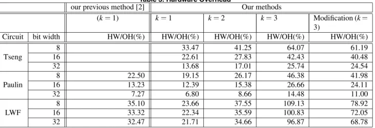
Table 2 shows the number of test MUXs and thru func- tion added in the DFT methods and Table 3 shows the hard- ware overhead (HW/OH). In these tables, column Modifi- cation shows results obtained by the modified DFT method discussed in Section 4.6. Notice that the hardware overhead in Table 3 does not contain that for TPGs and RAs added at PIs and POs since these are added in any BIST method. However, the hardware of case of k=3 includes that for one
LFSR that is added other than LFSRs at POs. The additional LFSR is necessary because each of the benchmark circuits has two POs while we require three RAs for case of k 3.
We can see, from Table 3, our method improves hard- ware overhead in case of k 1 compared with our previous method [2]. This proves effectiveness of the newly intro- duced method based on the cut edges (Stage1). Table 4 shows the number of test sessions. Table 4 shows natural trade-off between hardware overhead and test application time (i.e., the number of test sessions). Our method on k=2 can decrease the number of test sessions compared with our previous method [2]. Therefore, our method improves test application time. However the number of test sessions on k=3 is worse than we expected, because testing test MUXs requires additional test sessions. Table 3 and 4 show that the modified DFT method discussed in Section 4.6 works better for these benchmark circuits.
6 Conclusions
This paper proposed concurrent single-control testabil- ity of RTL data paths for BIST and a DFT method based on the testability. The advantages of our BIST method are high fault coverage, low hardware overhead, short test ap- plication time, and at-speed testability. Furthermore, this method can choose a trade-off between hardware overhead and test application time.
In the proposed DFT method, we deal with MUXs and operational modules equally. However, it is desired that MUXs and operational modules are tested in distinct test sessions when MUXs have shorter test sequences than op- erational modules. It is easy to modify our DFT method so that MUXs and operational modules are tested in dis- tinct test sessions. More generally, it is interesting to make scheduling with considering testability of each mod- ule (e.g., length of a test sequence). It is one of our future works to extend our DFT method so that testability of each module can be considered and to investigate its influence to test application time and hardware overhead. Another future works is to modify the DFT algorithm so that the resultant data path should satisfy timing constraints on the original data path; e.g., to avoid insertion of the DFT ele- ments on the critical path of the data path.
Acknowledgments
This work was supported in part by Semiconductor Tech- nology Academic Research Center (STARC) under the Re- search Project, by Japan Society for the Promotion of Sci- ence (JSPS) under the Grant-in-Aid for Scientific Research, and by Foundation of Nara Institute of Science and Technol- ogy under the Grant for Activity of Education and Research, by Foundation of Nara Institute of Science and Technology under the Grant for Activity of Education and Research. valuable discussion.
References
[1] M.Abramovici, M.A.Breuer, and
A.D.Friedman:Digital System Testing and Testable Design, Computer Science Press,(1999)
[2] T.Masuzawa, M.Idutsu, H.Wada,and H.Fujiwara:
”Single-control testability of RTL data paths for BIST,” Proc. 9th Asian Test Symposium, pp.210- 215(2000)
[3] B.Koenemann, J.Mucha,and G.Zwiehoff:”Built-in logic block observation techniques,” In Proc.1979 IEEE Test Conf., pp.37-41
Table 1. Circuit characteristics
#PI #PO #Reg #MUX #OP Area(8bit) Area(16bit) Area(32bit)
Tseng 3 2 6 7 7 858.6 1142.9 355.8
Paulin 2 2 7 11 4 2499.4 3818.9 735.0
LWF 2 2 5 5 3 8085.0 13778.9 1493.4
Table 2. Added MUX and Thru function our previous
method [2]
Our methods
(k 1) k 1 k 2 k 3 Modification
(k 3)
Circuit #MUX #THRU #MUX #THRU #MUX #THRU #MUX #THRU #MUX #THRU
Tseng 8 8 10 11 15 8 14 8
Paulin 8 5 7 6 8 8 14 7 12 7
LWF 4 3 2 4 4 4 11 3 7 2
Table 3. Hardware Overhead
our previous method [2] Our methods
(k 1) k 1 k 2 k 3 Modification (k
3)
Circuit bit width HW/OH(%) HW/OH(%) HW/OH(%) HW/OH(%) HW/OH(%)
8 33.47 41.25 64.07 61.19
Tseng 16 22.61 27.83 42.43 40.48
32 13.68 17.01 25.74 24.54
8 22.50 19.15 26.17 46.38 41.98
Paulin 16 13.23 12.39 15.38 26.66 24.11
32 7.27 6.80 8.66 14.48 11.00
8 35.10 23.66 37.55 109.13 78.92
LWF 16 33.32 22.34 35.59 100.83 72.05
32 32.47 21.71 34.66 96.87 68.78
Table 4. Test Session
our previous method [2] Our methods
(k 1) k 1 k 2 k 3 Modification (k
3)
Circuit session session session session session
Tseng 21 12 10 10
Paulin 23 22 12 10 10
LWF 12 10 6 7 6