Fault-dependent/independent Test Generation Methods for State Observable FSMs
Toshinori Hosokawa
†Ryoichi Inoue
††and Hideo Fujiwara
‡†College of Industrial Technology, Nihon University
1-2-1, Izumicho, Narashino, Chiba 275-8575, Japan
††Graduate School of Industrial Technology, Nihon University
1-2-1, Izumicho, Narashino, Chiba 275-8575, Japan
‡Graduate School of Information Science, Nara Institute of Science and Technology (NAIST)
8916-5, Takayama, Ikoma, Nara 630-0192, Japan
E-mail: † [email protected], ††[email protected],‡[email protected]
Abstract
Since scan testing is not based on the function of the circuit, but rather its structure, this method is considered to be a form of over testing or under testing. It is important to test VLSIs using the given function. Since the functional specifications are described explicitly in the FSMs, high test quality is expected by performing logical testing and timing testing. This paper proposes two test generation methods, a fault-independent test generation method and a fault-dependent test generation method, for state- observable FSMs. We give experimental results for MCNC’91 benchmark circuits. The quality and cost of the logic testing and timing testing for proposed test generation methods was evaluated.
keywords: State-observable FSMs, Fault-dependent test generation, Fault-independent test generation
1. Introduction
In recent years, Very Large Scale Integrated circuit (VLSI) testing has become increasingly important because the number of gates on VLSIs is rapidly increasing and their complexity is growing with advances in semiconductor technology. Currently, scan testing for the stuck-at fault model [1, 2] is one of the most popular test methods for VLSIs. However, it has been reported that scan testing for the stuck-at fault model may not detect defective VLSIs [4], and delay testing and at-speed functional testing can effectively improve test quality [3].
As mentioned above, scan testing is currently the most popular test method. Scan testing is based on the structure of the circuit rather than its function. In scan testing, the states of the circuits are transferred to invalid states by shift operation during the testing in order to detect faults. This method is considered to be a form of over testing and a yield loss of VLSIs may occur. In scan testing, faults are not detected by performing sequential operations of circuits. This testing is considered to be a form of under testing. Therefore, the test quality deteriorates, and outflow of defective VLSIs into the market may occur.
Recently, VLSIs are designed at the Register Transfer Level (RTL), and RTL circuits consist of a data path part and a controller part. The data path contains a hardware element and signal lines. The controller is represented by a finite state machine (FSM). A non-scan-based Design For Testability (DFT) method of data path parts is proposed in [5], whereas a non-scan-based DFT method for controller parts is proposed in [6]. At-speed testing is easily applicable, and test patterns for a stuck-at fault model are completely generated by non-scan-based DFT methods. In [7], a DFT method which is integrated the two DFT methods [5, 6] is proposed. As for the FSM, the circuit specification is described explicitly. Thus, it is expected that the test quality becomes high by performing a logical test and a timing test under the constraints of the circuit specifications. It was reported in [8] that state-observable and completely specified FSMs are thoroughly logically tested by performing all of the state transitions. Complete timing testing can be also applied by performing all pairs of state transitions at-speed.
This paper proposes two test generation methods, a fault-independent test generation method and a fault- dependent test generation method for state-observable FSMs.
2. State-observable FSMs
(Definition 1: State-observable FSMs)
When an initial state can be identified by observing an output sequence without being dependent on an input sequence, the FSM is said to be state-observable. More specifically, when an initial state can be identified by observing an output sequence of k length, the FSM is said to be k state-observable.
The DFT transformed an FSM to a one-state observable FSM by making the outputs of the status registers in the FSM observable. In this paper, a one-state observable FSM is hereinafter referred to simply as a state-observable FSM. A synchronous sequential circuit is synthesized from the FSM by logic synthesis. In the test for state-observable FSMs, the PI (primary input) value is applied to a state- 16th IEEE Asian Test Symposium
1081-7735/07 $25.00 © 2007 IEEE DOI 10.1109/ATS.2007.59
275
16th IEEE Asian Test Symposium
1081-7735/07 $25.00 © 2007 IEEE DOI 10.1109/ATS.2007.59
275
16th IEEE Asian Test Symposium
1081-7735/07 $25.00 © 2007 IEEE DOI 10.1109/ATS.2007.59
275
observable FSM, the state is then transferred from the current state to the next state, and the resulting PPI (pseudo primary inputs, which are the outputs of the status registers) and PO (primary outputs) values are observed.
3. Test Generation Method for State-
observable FSMs
3.1 Logical Testing (One-pattern Testing) (Definition 2: FSM logical test generation graph)
An FSM logical test generation graph is a directed graph G(V, E, r, s), where a vertex v ∈ V denotes a state. Each vertex has a label s: V → A (A = {PPI1PPI2…PPIm}, PPI1, PPI2, …, PPIm ∈ {0, 1}, where m denotes the number of status registers). The label s indicates the state assignment. For any vertices u, v ∈ V, an edge (u, v) ∈ E denotes the state transition from u to v, and each edge has a label r: E → B (B = {PI1PI2… PIn}, PI1, PI2, …, PIn ∈ {0, 1}, where n denotes the number of primary inputs). The label r indicates the input values for a state transition. (Definition 3: One-state transition coverage)
One-state transition coverage is defined as the ratio of the number of state transitions executed by a test sequence to the total number of state transitions in an FSM logical test generation graph. When state transitions are executed by a test sequence, the state transitions are said to be covered by the test sequence. In this paper, only state transitions specified in an FSM are used to calculate the one-state transition coverage. One-state transition coverage is then used as the measure of the test quality for logical testing.
3.1.1 Fault-independent Test Generation Method for Logical Testing
(Formulation 1a)
Input: a state-observable FSM.
Output: a test sequence such that the one-state transition coverage is 100%. (All of the state transitions in the FSM logical test generation graph are performed.) Optimization: minimization of the test length.
An FSM logical test generation graph is generated from the state-observable FSM and searches the path such that all of the edges are traversed at least once. If the path length is minimized, then the test length is also minimized. This test sequence can logically test a state-observable FSM completely.
3.1.2 Fault-dependent Test Generation Method for Logical Testing
In this paper, a single stuck-at fault model is considered as a representative of detectable fault models by logical testing.
(Definition 4: Detectable stuck-at faults on valid states) When a state is defined in a state-observable FSM and is reachable from the reset state, the state is called a valid state. Stuck-at faults detected by performing a state transition on a current state are referred to as detectable stuck-at faults on valid states.
(Formulation 1b) Input:
- a state-observable FSM.
- a one-pattern test set that can detect all detectable stuck-at faults on valid states.
Output: a test sequence for a state-observable FSM such that all detectable stuck-at faults on valid states are detected.
Optimization: minimization of the test length.
After logic synthesis, a combinational circuit part is extracted from the synthesized sequential circuit. The valid states are assigned to the PPI values as constraints. A constrained ATPG is performed on the stuck-at faults for a combinational circuit part and a one-pattern test set is generated. After that, an FSM logical test generation graph is generated and one-pattern tests are assigned to the corresponding edges of an FSM logical test generation graph. Finally, paths are searched on the FSM test generation graph such that all of the edges on which one- pattern tests are assigned are traversed at least once. If the path length is minimized, the test length is also minimized. 3.2 Timing Testing (Two-pattern Testing)
(Definition 5: FSM timing test generation graph) An FSM timing test generation graph is a directed graph G(V, E, s, d, t), where a vertex v ∈ V denotes a state transition. Each vertex has a label s: V → A, a label d: V → A(A = {PPI1PPI2… PPIm}, PPI1, PPI2,…, PPIm∈ {0, 1}, where m denotes the number of status registers), and a label t: V → B (B = {PI1PI2…PIn}, PI1, PI2, …, PIn∈ {0, 1}, where n denotes the number of primary inputs). The label s indicates the source state of the state transition, the label d indicates the destination state of the state transition, and the label t indicates input values for the state transition. For any vertices u, v ∈ V, an edge (u, v) ∈ E denotes that the destination state in u is the same as the source state in v. The edge (u, v) represents a continuous state transition pair
.
(Definition 6: Two-state transition coverage)
Two-state transition coverage is defined as the ratio of the number of continuous state transition pairs executed by a test sequence to the total number of continuous state transition pairs in an FSM timing test generation graph. When continuous state transition pairs are executed by a test sequence, the continuous state transition pairs are said to be covered by the test sequence. In this paper, only
276 276 276
continuous state transition pairs specified in an FSM are used to calculate the two-state transition coverage. Two- state transition coverage is used as the measure of the test quality for timing testing.
3.2.1 Fault-independent Test Generation Method for Timing Testing
(Formulation 2a)
Input: a state-observable FSM.
Output: a test sequence such that the two-state transition coverage is 100%. (All continuous state transition pairs in the FSM timing test generation graph are performed.)
Optimization: minimization of the test length.
An FSM timing test generation graph is generated from the state-observable FSM and searches the path such that all of the edges are traversed at least once. If the path length is minimized, then the test length is also minimized. This test sequence can perform a timing test on a state- observable FSM completely.
3.2.2 Fault-dependent Test Generation Method for Timing Testing
In this paper, a non-robust testable path delay fault model is considered as a representative of detectable fault models by timing testing. A non-robust testable path delay fault model is hereinafter referred to as a path delay fault. (Definition 7: Detectable path delay faults on the transition between valid states)
The transition between valid states refers to performing state transitions between valid states in state-observable FSMs. After a transition between valid states, path delay faults detected by performing a continuous state transition are defined as detectable delay faults on the transition between valid states.
Fig. 1 Example of an FSM
Fig. 2 FSM timing test generation graph
(Formulation 2b) Input:
- a state-observable FSM.
- a two-pattern test set that can detect all detectable path delay faults on the transition between valid states.
Output: a test sequence for a state-observable FSM such that all detectable path delay faults on the transition between valid states are detected.
Optimization: minimization of the test length.
After logic synthesis, a time expansion model [10] for two time frames is generated from a synthesized sequential circuit. The valid states are assigned to the PPI values as constraints. A constrained ATPG for path delay faults is performed for the time expansion model, and a two-pattern test set is generated. An FSM timing test generation graph is then generated and two-pattern tests are assigned to the corresponding edges of an FSM timing test generation graph. Finally, paths are searched on the FSM timing test generation graph such that all of the edges where two- pattern tests are assigned are traversed at least once. If the path length is minimized, then the test length is also minimized.
Example: Figure 2 shows an FSM timing test generation graph that is generated from the state-observable FSM shown in Figure 1 and a two-pattern test set, which can detect all detectable path delay faults on the transition between valid states for a time expansion model with two time frames. The state 00 is assigned to S0, the state 01 is assigned to S1, and the state 10 is assigned to S2. Each two-pattern test is assigned to the corresponding edge in this graph. For example, t5t6 is assigned to the edge that represents the continuous state transition pair, which is the state transition from the valid state 01 through the input value 0 to the valid state 00, and the state transition from the valid state 00 through the input value 1 to the valid state 10.
4. Experimental Results
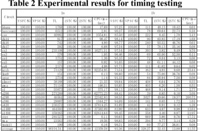
The test generation methods for Formulations 1a, 1b, 2a and 2b were implemented and were applied to MCNC’91 benchmark circuits [9].
Table 1 shows the experimental results of the test generation methods for the logical testing proposed in this paper. In Table 1, 1a denotes the fault-independent test generation method for logical testing, and 1b denotes the fault-dependent test generation method for logical testing. Table 2 shows the experimental results of the test generation methods for timing testing proposed in this paper. In Table 2, 2a denotes the fault-independent test generation method for timing testing, and 2b denotes the fault-dependent test generation method for timing testing.
S0 S1
S2 0 0
1 0
1 1 RESET
00→01 0
00→10 1
01→00 0
01→10 1
10→10 0
10→00 1
RESET RESET
t1t2
t3t4 t5t6
277 277 277
In Tables 1, and 2, Circuit, TL, VSFC, 1STC, VPSC, 2STC, and CPU time denote the circuit name of the FSM, the test length, the fault coverage of detectable stuck-at faults on valid states, the one-state transition coverage, the fault coverage of detectable path delay faults on transition between valid states, two-state transition coverage, and the time for the test generation, respectively.
For 1a, since the one-state transition coverage is 100%, the logical fault model including stuck-at faults can be completely tested. 1a is applicable to FSMs that have less than 1,000 state transitions with reasonable CPU time and test length (maximum: 1,107). However, the test length for FSMs that have many state transitions increases drastically. Although the average two-state transition coverage was as low as 12.9%, the test sequence detected an average of 85.1% of the path delay faults that were detectable on transition between valid states. Thus, 1a was found to have a comparatively high detection capability for path delay faults. Although the average two-state transition coverage for 1b was also as low as 8.1%, the test sequence detected an average of 67.4% of the path delay faults that were detectable on transition between valid states.
For 2a, since both the one-state transition coverage and the two-state transition coverage are 100%, the logical fault model including stuck-at faults and the timing fault model including path delay faults can be completely tested. 2a is applicable to FSMs that have less than 1,000 state transitions with reasonable CPU time and test length (maximum: 6,512). However, the test lengths for FSMs that have many state transitions drastically increase. The test length of 2b compared to 1b was an average of 2.3 times longer, and the one-state transition coverage was an average of 24.7% higher. However, the fault coverage for detectable stuck-at faults on valid states was an average of 93.3%. 2b could not completely test stuck-at faults.
5. Conclusion
This paper proposed both a fault-independent test generation method and a fault-dependent test generation method for state observable FSMs. This paper also
proposed one-state transition coverage as the measure of test quality for logical testing and two-state transition coverage as the measure of test quality for timing testing. The quality and cost of the logic testing and timing testing for proposed test generation methods was evaluated for MCNC’91 benchmark circuits.
References
[1] H. Fujiwara, “Logic Testing and Design for Testability,” The MIT Press, 1985.
[2] M. Abramovici, M. A. Breuer, and A. D. Friedman, “Digital systems testing and testable design,” IEEE Press, 1995. [3] A. Krstic, and K.-T. Cheng, “Delay Fault Testing for VLSI
Circuits,” Kluwer Academic Publishers, 1998.
[4] P.C. Maxwell, R.C. Aitken, R. Kollitz, and A. C. Brown,
“IDDQ and AC Scan: The War Against Unmodelled Defects,” Proc. of IEEE Int. Test Conf., pp.250-258, Oct., 1996.
[5] H. Wada, T. Masuzawa, K.K. Saluja, and H. Fujiwara,
“Design for strong testability of RTL data paths to provide complete fault efficiency,” Proc. of 13th Int. Conf. on VLSI Design, pp.300-305, 2000.
[6] S. Ohtake, T. Masuzawa, and H. Fujiwara, "A non-scan approach to DFT for Controllers Achieving 100% Fault Efficiency," Journal of Electronic Testing: Theory and Applications (JETTA), Vol. 16, No. 5, pp.553-566, Oct. 2000.
[7] S. Ohtake, H. Wada, T. Masuzawa and H. Fujiwara, " A non-scan DFT method at register-transfer level to achieve complete fault efficiency, " IEEE Proc. Asian South Pacific Design Automation Conference, pp.599-604, 2000.
[8] H. Fujiwara, and K. Kinoshita, “Design of Diagnosable Sequential Machines Utilizing Extra Outputs,” IEEE Trans. on Computers, Vol. C-23, pp.138-145, Feb., 1974.
[9] S. Yang, "Logic synthesis and optimization benchmarks user guide," Technical Report 1991-IWLS-UG-Saeyang, Microelectronics Center of North Carolina, 1999.
[10] T. Inoue, T. Hosokawa, T. Mihara,, and H. Fujiwara, “An optimal time expansion model based on combinational ATPG for RT level circuits”, IEEE Proc. Asian Test Symp., pp.190-197 , Dec. 1998.
Table 1 Experimental results for logical testing Table 2 Experimental results for timing testing
bbara 1 00.00 8 4.72 2 07 10 0.0 0 14 .79 0 .36 1 00.00 68.05 5 1 22.50 4.38 0.1 4 bee cou nt 1 00.00 7 3.83 1 20 10 0.0 0 21 .59 0 .11 1 00.00 42.06 3 0 41.07 9.85 0.0 6 cse 1 00.00 8 2.70 68 13 10 0.0 0 0 .00 54 .78 1 00.00 59.41 15 3 6.30 0.81 0.8 6 dk14 1 00.00 8 3.94 84 10 0.0 0 17 .41 0 .38 1 00.00 70.54 5 7 69.64 1 1.16 0.3 1 dk16 1 00.00 7 8.71 1 62 10 0.0 0 34 .49 0 .14 1 00.00 62.96 9 0 62.98 1 9.91 0.0 8 dk17 1 00.00 8 4.72 63 10 0.0 0 34 .38 0 .08 1 00.00 76.39 4 2 71.88 2 5.78 0.0 3 ex1 1 00.00 8 5.88 296 04 10 0.0 0 0 .73 167 .67 1 00.00 63.11 12 9 1.26 0.13 0.6 6 ex3 1 00.00 8 8.29 93 10 0.0 0 46 .25 0 .05 1 00.00 83.10 5 4 77.50 3 5.00 0.0 5 ex4 1 00.00 9 2.05 11 07 10 0.0 0 3 .48 0 .14 1 00.00 78.42 4 5 5.02 1.38 0.0 5 ex5 1 00.00 8 5.72 90 10 0.0 0 48 .53 0 .05 1 00.00 67.13 5 1 77.78 3 6.76 0.0 3 ex6 1 00.00 8 8.72 3 84 10 0.0 0 7 .77 0 .25 1 00.00 57.85 4 5 16.80 3.48 0.0 8 ke yb 1 00.00 8 2.08 82 53 10 0.0 0 2 .01 838 .25 1 00.00 62.74 20 7 5.18 0.61 1 2.63 lion9 1 00.00 6 4.29 39 10 0.0 0 26 .47 0 .05 1 00.00 57.15 2 1 52.78 1 8.38 0.0 5 opu s 1 00.00 9 2.85 9 21 10 0.0 0 2 .19 0 .17 1 00.00 84.92 5 7 16.88 3.44 0.0 3 plan et 1 00.00 9 6.23 121 38 10 0.0 0 3 .01 2 .52 1 00.00 72.01 19 8 3.22 0.95 0.0 8 pm a 1 00.00 6 7.04 124 98 10 0.0 0 1 .28 7 .17 1 00.00 56.04 15 0 2.43 0.45 0.1 1 s1 1 00.00 8 7.62 89 28 10 0.0 0 1 .35 11 .67 1 00.00 62.02 14 4 2.81 0.45 0.4 1 s2 08 1 00.00 10 0.00 301 44 10 0.0 0 1 .56 445 .56 1 00.00 92.58 12 0 2.60 0.20 1.2 0 s2 98 1 00.00 8 6.59 102 54 10 0.0 0 24 .86 201 .44 1 00.00 58.42 85 2 32.68 8.21 7.0 9 s3 86 1 00.00 9 5.04 58 95 10 0.0 0 2 .17 19 .73 1 00.00 68.32 10 2 6.13 0.71 0.2 8 s4 20 1 00.00 10 0.00 301 53 10 0.0 0 1 .52 306 .22 1 00.00 89.29 12 0 2.60 0.23 1.0 0 s1 488 1 00.00 9 0.83 862 02 10 0.0 0 1 .99 915 .47 1 00.00 61.98 26 7 2.17 0.28 1.7 6 s1 494 1 00.00 9 6.88 872 40 10 0.0 0 2 .08 1 481 .38 1 00.00 77.78 24 3 1.98 0.25 1.9 2 styr 1 00.00 6 9.58 425 07 10 0.0 0 0 .86 506 .50 1 00.00 47.97 21 0 1.36 0.18 1.5 6 tma 1 00.00 7 4.56 43 56 10 0.0 0 1 .85 1 .16 1 00.00 52.93 10 5 3.75 0.84 0.0 6 train11 1 00.00 8 2.10 63 10 0.0 0 34 .03 0 .03 1 00.00 80.60 4 5 86.36 2 9.17 0.0 1 average 1 00.00 8 5.19 145 50.69 10 0.0 0 12 .95 190 .82 1 00.00 67.45 138 .00 25.99 8.19 1.1 7
1 b
T L V P S C (%) V S F C (%) C irc uit
1a
1S T C (% )2S T C (%) T L 1 S T C (%)2S T C (% )
C P U tim e (sec) C P U tim e
(se c)
V P S C (% ) V S F C (%)
bbara 100 .0 0 10 0.0 0 1 768 1 00.00 1 00.00 17 .6 9 9 7.2 5 10 0.0 0 11 1 48 .1 3 10 .4 2 0.6 1 bee co unt 100 .0 0 10 0.0 0 6 512 1 00.00 1 00.00 2 .9 1 9 0.3 7 10 0.0 0 7 8 69 .6 4 22 .7 3 0.1 6 cse 100 .0 0 10 0.0 0 40 882 1 00.00 1 00.00 3 554 .8 1 8 5.5 0 10 0.0 0 22 2 8 .4 5 1 .7 0 3.1 3 dk14 100 .0 0 10 0.0 0 817 1 00.00 1 00.00 98 .4 7 9 8.1 4 10 0.0 0 9 0 83 .9 3 17 .1 9 1.6 9 dk16 100 .0 0 10 0.0 0 742 1 00.00 1 00.00 4 .8 0 9 8.7 7 10 0.0 0 24 0 93 .5 2 46 .7 6 0.6 1 dk17 100 .0 0 10 0.0 0 292 1 00.00 1 00.00 0 .8 8 9 7.5 4 10 0.0 0 5 7 78 .1 3 35 .1 6 0.0 9 ex1 100 .0 0 10 0.0 0 2 35 108 1 00.00 1 00.00 10 271 .5 1 9 7.5 4 10 0.0 0 39 3 3 .8 2 0 .4 9 9.7 0 ex3 100 .0 0 10 0.0 0 178 1 00.00 1 00.00 1 .0 5 9 6.4 6 10 0.0 0 6 9 65 .0 0 52 .5 0 0.1 1 ex4 100 .0 0 10 0.0 0 3 751 1 00.00 1 00.00 1 .3 6 9 5.3 5 10 0.0 0 7 2 8 .0 4 3 .1 3 0.0 6 ex5 100 .0 0 10 0.0 0 157 1 00.00 1 00.00 0 .9 2 9 1.0 5 10 0.0 0 4 8 61 .1 1 44 .1 2 0.0 8 ex6 100 .0 0 10 0.0 0 2 173 1 00.00 1 00.00 4 .9 8 9 7.7 3 10 0.0 0 11 1 41 .0 2 9 .6 4 0.0 2 ke yb 100 .0 0 10 0.0 0 73 129 1 00.00 1 00.00 82 254 .9 5 7 3.5 4 10 0.0 0 16 2 4 .9 3 0 .6 8 2 0.4 4 lion9 100 .0 0 10 0.0 0 151 1 00.00 1 00.00 0 .1 3 9 6.8 0 10 0.0 0 5 4 75 .0 0 36 .7 6 0.0 8 op us 100 .0 0 10 0.0 0 2 734 1 00.00 1 00.00 1 .1 4 9 1.3 3 10 0.0 0 8 4 20 .9 4 7 .5 0 0.0 8 plan et 100 .0 0 10 0.0 0 38 188 1 00.00 1 00.00 21 .5 5 9 9.8 4 10 0.0 0 40 8 6 .6 4 2 .7 6 0.3 3 pm a 100 .0 0 10 0.0 0 71 116 1 00.00 1 00.00 146 .5 1 9 5.8 5 10 0.0 0 40 5 6 .2 0 1 .5 8 0.5 3 s1 100 .0 0 10 0.0 0 55 873 1 00.00 1 00.00 575 .1 7 9 8.1 3 10 0.0 0 46 8 9 .1 4 1 .7 1 2.7 7 s2 08 100 .0 0 10 0.0 0 2 73 289 1 00.00 1 00.00 62 772 .2 3 8 8.4 1 10 0.0 0 3 9 0 .8 5 0 .1 0 3.0 9 s2 98 100 .0 0 10 0.0 0 46 561 1 00.00 1 00.00 22 542 .8 3 9 8.5 5 10 0.0 0 3 027 49 .6 6 19 .5 7 20 0.7 2 s3 86 100 .0 0 10 0.0 0 29 887 1 00.00 1 00.00 1 044 .2 7 9 4.0 9 10 0.0 0 14 1 8 .0 5 1 .7 2 1.0 1 s4 20 100 .0 0 10 0.0 0 2 30 272 1 00.00 1 00.00 37 814 .2 5 8 1.8 9 10 0.0 0 4 2 0 .9 1 0 .1 2 1.2 8 s1 488 100 .0 0 10 0.0 0 4 64 593 1 00.00 1 00.00 37 582 .0 9 8 3.9 0 10 0.0 0 63 3 4 .8 7 0 .9 8 1 2.6 1 s1 494 100 .0 0 10 0.0 0 4 59 265 1 00.00 1 00.00 62 614 .6 4 9 0.4 5 10 0.0 0 55 8 4 .4 0 0 .8 7 2 2.9 7 styr 100 .0 0 10 0.0 0 2 81 527 1 00.00 1 00.00 0 .1 1 9 0.6 3 10 0.0 0 66 9 3 .8 6 0 .7 6 1 7.7 2 tma 100 .0 0 10 0.0 0 23 563 1 00.00 1 00.00 19 .5 6 9 8.8 3 10 0.0 0 29 4 9 .7 7 3 .1 4 0.2 8 train11 100 .0 0 10 0.0 0 190 1 00.00 1 00.00 0 .1 6 9 9.3 1 10 0.0 0 6 0 77 .2 7 36 .8 1 0.0 8 average 100 .0 0 10 0.0 0 901 04.54 1 00.00 1 00.00 12 359 .5 8 9 3.3 6 10 0.0 0 328 .27 32 .4 3 13 .8 0 1 1.5 5
2 b 2a
C ircuit
C P U time (sec) V P S C (%) T L 1S T C (%) V S F C (% )
V S F C (% )V P S C (%) T L 1 S T C (%)2 S T C (%) C P U time
(se c)
2S T C (%)
278 278 278