An Optimal Test Bus Design for Transparency-based SoC Test
Tomokazu Yoneda†, Akiko Shuto‡
∗, Hideyuki Ichihara‡, Tomoo Inoue‡, and Hideo Fujiwara†
†Graduate School of Information Science, Nara Institute of Science and Technology
Kansai Science City, 630-0192, Japan
{yoneda, fujiwara}@is.naist.jp
‡Graduate School of Information Science, Hiroshima City University
3-4-1, Ozuka-higashi, Asaminami-ku, Hiroshima, 731-3194, Japan
{ichihara, tomoo}@im.hiroshima-cu.ac.jp
Abstract
We present a graph model and an ILP model for opti- mal test bus design for transparency-based SoC testing. The proposed method is an extension of [12] so that not only the system-level cost but also the core-level cost can be simul- taneously taken into consideration during the optimization process. We also relax the constraints by considering test data flows and extend it to be able to handle the case where cores can not be made transparent due to IP protection. The proposed ILP model can represent various problems includ- ing the same problem as [12] and produce better results. Experimental results show the effectiveness and flexibility of the proposed method compared to [12].
keywords: SoC, test access mechanism, transparency, ILP
1 Introduction
The systems-on-chip (SoC) design strategies help us to reduce the time-to-market and design cost for new products significantly. On the other hand, testing of SoCs gives rise to difficult and time consuming problems due to the increas- ing design complexity[1]. The main difficulty of SoC test- ing is how to propagate test data from(to) the outside of the SoC to(from) cores which are deeply embedded inside the SoC.
A number of approaches have addressed wrapper design [2, 3, 4] which are IEEE 1500 [5] compliant. Similarly, sev- eral test access mechanism (TAM) architectures have been proposed [6, 7, 8, 9, 10, 11, 12]. TAM architecture can be roughly classified into two types:1)TAM dedicated to test including TestBus[6, 7] and TESTRAIL[8], and 2)TAM not dedicated to test including the method re-using func- tional buses[13, 14, 15], the methods re-using functional networks[16, 17] and the methods based on transparency[9, 10, 11, 12]. The methods re-using functional buses and net- works assume that cores are accessible by using the buses and the networks while the transparency-based method deal with SoCs without such direct accessible connections. Transparency-based TAM can be further classified into two types:1)single-cycle throughput transparency[11, 12] and
∗She is currently with Sony Semiconductor Kyushu Co., Ltd.
2)multi-cycle throughput transparency[9, 10]. Single-cycle throughput transparency has two main advantages com- pared to multi-cycle throughput transparency: 1)short test application time and 2) ability to preserve timing infor- mation for test sequences. The authors in [11, 12], how- ever, considered core-level transparency design problem and system-level TAM design problem separately. In other words, the authors first tackled only with the design for transparency problem without considering the system level connectivity information. After that, the authors worked on the optimization problem to minimize system-level cost for TAM design without considering the cost of making cores transparent.
In this paper, we extend the method proposed in [12] which is based on integer linear programming (ILP) formu- lation so that not only the system-level cost for TAM design but also the core-level cost for making cores transparent can be simultaneously taken into consideration during the opti- mization process. Moreover, we also relax the constraints by considering test data flows and extend it to be able to handle the case where cores can not be made transparent due to IP protection and so on. The proposed method con- sists of an extended graph modeling and an ILP formula- tion. We can represent various problems including the same problem as [12] by setting constant parameters in the pro- posed ILP model appropriately. Experimental results show the effectiveness and flexibility of the proposed method.
The rest of this paper is organized as follows. We dis- cuss the related work proposed in [12] in Section 2. Section 3 shows the proposed optimal test bus design method for transparency-based SoC test including graph modeling and ILP modeling. Experimental results are discussed in Sec- tion 4. Finally, Section 5 concludes this paper.
2 Related Work[12]
In [12], single-cycle transparency is achieved by embed- ding multiplexers in the behavioral models described using a hardware description language. An example is shown in Fig. 1. An additional control input T is used to switch a core from the normal mode (T = 0) to transparent mode (T = 1). IEEE 7th Workshop on RTL and High Level Testing (WRTLT'06), pp. 21-26, November, 2006.
Figure 1. (a) Original circuit, (b) Circuit with em- bedded multiplexers
Figure 2. Example SoCS1and its system graph
An additional 2 bit output port Y is added to ensure com- plete transparency. In general, a core may be required to expand its input/output ports for transparent access of other cores, not just for itself. Therefore, [12] proposed a method to minimize the overhead of additional ports and associ- ated interconnect area. The method analyzes SoC testing requirements and formulates it as an ILP problem.
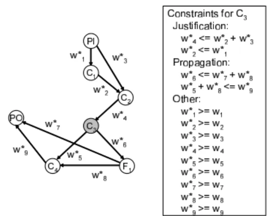
The method first constructs a weighted directed system graph whose vertices are the cores and fanout points of functional interconnects in the SoC and whose edges are functional interconnects between the cores. The weight of an edge (Ci,Cj) denotes the total width of the buses con- necting Cito Cj. An example SoC S1and the corresponding system graph are shown in Fig. 2. Next, it breaks all cycles in the system graph by solving the minimum feedback ver- tex set problem. The acyclic SoC and the corresponding system graph G are shown in Fig. 3.
Then, it constructs the same weighted directed graph G∗ as G except for the weights of edges. The new edge weights can be determined by generating test graph for each core. For core Cj, the test graph Gj ⊆G∗ contains a vertex Ci
if either of the two conditions holds: i)Cilies on a directed path from the source vertex to Cj, or ii) Cilies on a directed path from Cjto the sink vertex. Similarly, an edge (Ci,Cj) belongs to Gjif it either lies on a path from the source vertex to Cjor on a path from Cjto the sink vertex. Fig. 4(a) shows the test graph for C3in S1. For each test graph Gj, it imposes
Figure 3. Acyclic SoC and its system graphG
Figure 4. Test graphG3and constraints forC3
a set of constraints on edge weights for the edges in G∗as follows.
1. justification constraints: If Ci lies on a path from the source vertex to Cjin Gj, then the sum of the weights of the edges directed away from Ciin Gjmust not ex- ceed the sum of the weights of the edges incident on Ci.
2. propagation constraints: If Ci lies on a path from Cj
to the sink vertex in Gj, then the sum of the weights of the edges incident on Ciin Gjmust not exceed the sum of the weights of the edges directed away from Ci. Moreover, for each edge, the weight of the edge in G must not exceed the weight of the edge in G∗ (i.e., w∗k ≥ wk). The constraints on the edge weights for C3 are shown in Fig. 4(b). The total increase in the interconnect for S1 is given by Cost =!i(w∗i−wi) where w∗is are variables whose values are to be determined and wis are known constants. Therefore, the problem to minimize interconnect area can be expressed an ILP model where the objective is to mini- mize Cost subject to the constraints on the edge weights.
3 Optimal Test Bus Design
3.1 ContributionsIn this section, we present a graph modeling and ILP modeling method for optimal test bus design. The proposed method is an extension of [12] with respect to the follow- ing three points: (1)cost for transparency, (2) test data flow and (3)additional bypass path. Before describing the details
of graph and ILP modeling, we explain effectiveness of the above-mentioned extensions severally.
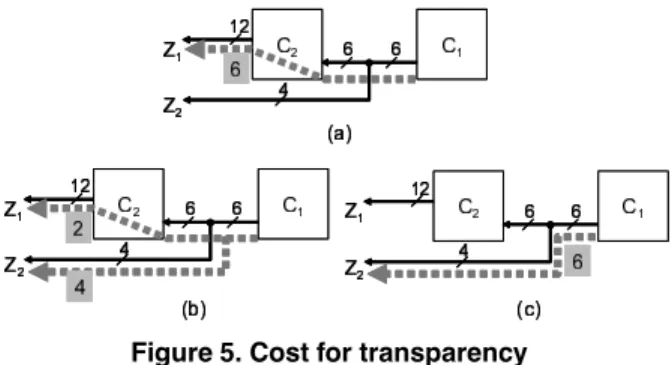
(cost for transparency) The method proposed in [12] con- sidered to minimize only the overhead of additional inter- connect area. In other words, the cost of making cores transparent is ignored during the optimization. However, we can get better solution if not only the cost of additional interconnect area but also the cost of making cores transpar- ent are taken into account simultaneously. Fig. 5 is a sim- ple example. We can satisfy the propagation constraints for C1without additional interconnect by using the dotted line shown in Fig. 5(a). Though the cost of additional intercon- nect area is 0, we actually have to pay the cost for making C26-bit transparent. Suppose that the cost for making C21- bit transparent is 1, then the cost is 6. On the other hand, if we consider the cost of making C2transparent as well as the cost of additional interconnect area, then we can get better solution shown in Fig. 5(b) where the cost is 2. Moreover, if we assume that the cost for making C21-bit transparent is 2 and the cost for 1-bit additional interconnect is 1, then we can get another solution shown in Fig. 5(c). From this example, we can say that it is important and effective to consider the cost of making cores transparent as well as the cost of additional interconnect area simultaneously during optimization.
(test data flow) In [12], for each edge, the weights of the edge in G must not exceed the weight of the edge in G∗, i.e., w∗i ≥wi. However, this is not always necessary in or- der to satisfy the justification and propagation constraints for each core. For example, in Fig. 4, we need w∗5+w∗8≤w∗9 as a propagation constraint for C3. If we impose the con- straint w∗i ≥ wi upon every edge, then, the cost to satisfy the propagation constraints is 6 (w∗5 = 12,w∗6 = 8,w∗7 = 4,w∗8 = 6,w∗9 = 18). Indeed, for each core, the edges di- rected away from the core vertex and the edges incident on the core vertex must be subject to the constraints w∗i ≥ wi in order to justify/propagate test patterns/response to/from the cores. On the other hand, however, other edges may have bus width enough for the test data flow (or the justi- fication and propagation) of the core, and accordingly they can be under no such constraints during the test. In this example, we only need the following three constraints:(1) w∗4 ≥ w4, (2) w∗5 ≥ w5 and (3) w∗6 ≥ w6, and the prop- agation constraints for C3 can be satisfied with cost of 4. (w∗5=12,w∗6=8,w7∗=4,w∗8=4,w∗9 =16).
(additional bypass path) In the SoC design strategies, the behavioral models described using a hardware description language are not always available due to IP protection and so on. Even if it is available, it may happen that the to- tal cost (including area, time for synthesis and layout etc.) of making cores transparent by embedding multiplexers is higher than that of bypass paths added outside the cores by
Figure 5. Cost for transparency
non-embedded multiplexers. Moreover, it may happen that the cost of single-core bypass path (bypass path from a core input to the core output) is higher than that of multi-core by- pass path (bypass path from a core input to another core out- put) ) due to the layout related issue and so on. Therefore, considering the transparent paths as well as bypass paths is important and effective for cost optimization.
3.2 Graph Modeling
In this section, we introduce an extended system graph for optimal test bus design such that the above three points can be taken into consideration during optimization. First of all, we break all cycles in the system by solving the minimum feedback vertex set problem in similar way to [12] shown in Section 2. Next, we construct an extended weighted directed acyclic system graph G = (V,E,w) as follows.
• V = Vport∪Vf an∪{vPI} ∪ {vPO}where
Vport: the set of all input and output ports of cores, Vf an: the set of all fanout points,
vPI : the vertex corresponds to the primary inputs of the system, and
vPO: the vertex corresponds to the primary outputs of the system.
• E = Ef∪Et∪Es∪Emwhere
Ef : the set of all functional interconnections, Et: the set of all transparent paths,
Es: the set of all single-core bypass paths, and Em: the set of all multi-core bypass paths.
• w: E → Z
If e ∈ Ef, then w(e) denotes the width of the func- tional interconnect. Otherwise, w(e) is equal to 0. The extended acyclic system graph G corresponds to Fig. 3 is shown in Fig. 6. In Fig. 6, we consider two multi-core by- pass paths which correspond to e24 and e25, respectively. The edges correspond to functional interconnects and trans- parency paths (i.e., e ∈ Ef∪Et) are shown as straight lines, and the edges correspond to bypass paths (i.e., e ∈ Es∪Em) are shown as curved lines.
Then, we construct the same weighted directed graph G∗ = (V,E,w∗) as G except for the weights of edges. The new edge weights in G∗ can be determined by solving the
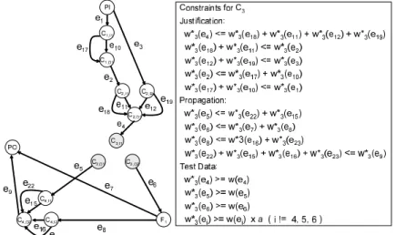
Figure 6. Extended system graphG Figure 7. Test graphG3and constraints forC3
ILP problem formulated in the next section.
3.3 ILP Formulation
In this section, we present an ILP model for optimal test bus design. The new edge weights can be determined by generating test graph for each core. For core Cj , the test graph Gj = (Vj,Ej,w∗j) ⊆ G∗contains vertices and edges reachable to(from) the input(output) ports of Cj. For each edge e ∈ Ej, w∗j(e) represents a test data flow on e for Cj. For each test graph Cj, we impose a set of constraints on test data flows for the edges in Ej. These constraints are of three types: (1)justification constraints, (2)propagation constraints and (3)test data constraints shown as follows.
1. justification constraints: For each vertex v ∈ Vjreach- able to the input ports of Cj, the sum of the test data flows of the edges directed away from v must not ex- ceed the sum of the test data flows of the edges incident on v.
2. propagation constraints: For each vertex v ∈ Vjreach- able from the output ports of Cj, the sum of the test data flows of the edges incident on v must not exceed the sum of the test data flows of the edges directed away from v.
3. test data constraints: If e ∈ Ejis the edge incident on the input ports of Cj or the edge directed away from the output ports of Cj, then w∗j(e) ≥ w(e). Otherwise, w∗j(e) ≥ w(e) × a where a is a binary constant. If we set the binary constant a to 1, we can represent the same constraints as [12] where every edge e ∈ Ej is constrained by w∗j(e) ≥ w(e). On the other hand, if we set ato 0, we can relax the constraints by considering the test data flows where only the edges e ∈ Ejincident on the input ports of a core Cj under test and directed away from the output ports of Cj are constrained by w∗j(e) ≥ w(e). The constraints on the test data flows for C3are shown in Fig. 7.
The total cost to satisfy the constraints is given by Cost ="
e∈E
c(e) · (max (w∗(e),w(e)) − w(e)) (1) where c(e) is a known constant for each e and denotes the cost for 1-bit increase of e and w∗(e) denotes the maximum test data flow on e (i.e., w∗(e) = maxj(w∗j(e))). Therefore, the problem to minimize total cost can be expressed an ILP model where the objective is to minimize Cost subject to the constraints on the edge weights.
The advantage of the proposed ILP model is that we can represent various situations including the same problem as [12] by setting c(e). For example, the proposed ILP model can be represent the same problem as [12] where the cost of transparency is 0 and we cannot consider the bypass paths by setting c(e) as follows.
• c(e) = 1 if e ∈ Ef,
• c(e) = 0 if e ∈ Et,
• c(e) = ∞ if e ∈ Es∪Em
We can also consider the case where both the cost of addi- tional interconnections and transparency are taken into ac- count by setting c(e) ! 0 for e ∈ Et. An example setting for this case is shown as follows.
• c(e) = 1 if e ∈ Ef,
• c(e) = 1 if e ∈ Et,
• c(e) = ∞ if e ∈ Es∪Em
Moreover, by setting c(e) as follows, we can consider the case where transparency cannot be achieved due to IP pro- tection and only bypass paths are allowed to add.
• c(e) = 1 if e ∈ Ef,
• c(e) = ∞ if e ∈ Et,
• c(e) ! ∞ if e ∈ Es∪Em
Of course, we can set c(e) to different value for every e ∈ E depending on the given SoC.
4 Experimental Results
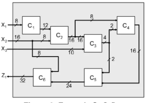
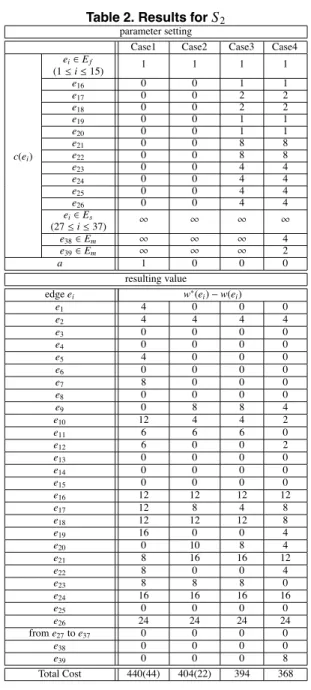
In this section, we present experimental results for SoC S1shown in Fig. 2 and SoC S2 shown in Fig. 8 and Fig. 9.
Figure 8. Example SoCS2
We used the lp solve package from Eindhoven University of Technology [18] for the experiments. We made exper- iments for the following four cases. All the experimental results can be obtained within 0.1 sec. on a SunBlade 2000 workstation (1.05 GHz with 8GB RAM).
Case1: Same optimization problem as [12] where (1)bypass paths are not allowed and (2)the objective is to minimize only the cost of additional interconnect area.
Case2: Same optimization problem as Case1 except for re- laxing the constraints (i.e., a = 0 in Case2 while a = 1 in Case1).
Case3: Same optimization problem as Case2 except for tak- ing the cost of making cores transparent into consideration to minimize the total cost.
Case4: Same optimization problem as Case3 except for tak- ing the multi-core bypass paths into consideration.
Table 1 shows the results for S1where we set the same cost (i.e., c(e) = 1) to every edge e except multi-core by- pass paths (e ∈ Em). In Case1 and Case2, the number in parentheses denotes the cost of additional interconnect area and the number outside parentheses denotes the total cost including the cost of making cores transparent, respec- tively. We can observe the effect of relaxing the constraints by comparing Case2 with Case1. We can reduce the cost of additional interconnect area from 23 to 17. Although the effect of considering the cost for transparency as well as the cost for additional interconnect area simultaneously cannot be observed (compare Cases 2 and 3), taking two multi-core bypass paths into consideration (Case4) achieved a signifi- cant reduction in the total cost to 74. We can observe no- ticeable trends for S2 in Table 2. In particular, by compari- son Cases 2 and 3, we can observe the effect of considering both the core-level cost for transparency and the system- level cost for additional interconnect area simultaneously. In these results, we did not show the case where cores can not be made transparent and bypass paths are allowed to add. However, the same results can be obtained for every case in terms of the total cost if we exchange c(e) for e ∈ Et
with c(e) for e ∈ Eb.
Figure 9. Extended system graph forS2
5 Conclusion
We proposed a graph model and an ILP model for op- timal test bus design for transparency-based SoC testing. The proposed method is an extension of [12] so that not only the cost for system-level interconnet area but also the cost for transparency can be simultaneously taken into con- sideration during optimization process. We also extended it to be able to handle the case where cores can not be made transparent due to IP protection. Moreover, we relaxed the constraints by considering the test data flows in the pro- posed ILP formulation. Therefore, the proposed ILP model is flexible in the sense that it can represent various prob- lems including [12] by setting constant parameters, and it can produce better results compared to [12] in terms of total cost.
Acknowledgments
This work was supported in part by Japan Society for the Promotion of Science (JSPS) under Grants-in-Aid for Sci- entific Research B(2)(No. 15300018) and for Young Scien- tists(B)(No.18700046).
References
[1] Y. Zorian, E. J. Marinissen and S. Dey, “Testing embedded- core based system chips,” Proc. International Test Confer- ence, pp. 130–143, Oct. 1998.
[2] V. Iyengar, K. Chakrabarty and E. J. Marinissen, “Test Wrap- per and test access mechanism co-optimization for system- on-chip,” Journal of Electronic Testing: Theory and Appli- cations, pp. 213–230, Apr. 2002.
[3] W.Zou,S.R.Reddy,I.Pomeranz and Y.Huang, “SOC Test Scheduling Using Simulated Annealing,” Proc. 21th VLSI Test Symposium,pp. 325–329,May 2003.
[4] E. J. Marinissen, S. K. Goel, and M. Lousberg, “Wrapper Design for Embedded Core Test,” Proc. International Test Conference, pp. 911–920, Oct. 2000.
Table 1. Results forS1 parameter setting
Case1 Case2 Case3 Case4 ei∈Ef
(1 ≤ i ≤ 9) 1 1 1 1
ei∈Et
(10 ≤ i ≤ 16) 0 0 1 1
ei∈Es
(17 ≤ i ≤ 23) ∞ ∞ ∞ ∞
e24∈Em ∞ ∞ ∞ 4
c(ei)
e25∈Em ∞ ∞ ∞ 2
a 1 0 0 0
resulting value
edge ei w∗(ei) − w(ei)
e1 0 0 0 0
e2 2 0 0 0
e3 0 0 0 0
e4 15 13 13 7
e5 0 0 0 0
e6 0 0 0 0
e7 0 4 4 4
e8 0 0 0 0
e9 6 0 0 0
e10 17 15 15 15
e11 17 15 15 9
e12 3 3 3 3
e13 12 12 12 12
e14 8 6 6 0
e15 12 12 12 12
e16 6 0 0 0
from e17to e23 0 0 0 0
e24 0 0 0 0
e25 0 0 0 6
Total Cost 98(23) 80(17) 80 74
[5] E.J. Marinissen, R. Kapur, M. Lousberg, T. McLaurin, M. Ricchetti and Y. Zorian, “On IEEE P1500’s Standard for Em- bedded Core Test,” Journal of Electronic Testing: Theory and Applications, pp. 365–383, Aug. 2002.
[6] T. Ono, K. Wakui, H. Hikima, Y. Nakamura and M. Yoshida,
“Integrated and automated design-for-testability implemen- tation for cell-based ICs,” Proc. 6th Asian Test Symposium, pp. 122–125, Nov. 1997.
[7] P. Varma and S. Bhatia, “A structured test re-use method- ology for core-based system chips,” Proc. International Test Conference, pp. 294–302, Oct. 1998.
[8] E. Marinissen, R. Arendsen, G. Bos, H. Dingemanse, M. Lousberg and C. Wouters, “A structured and scalable mech- anism for test access to embedded reusable cores,” Proc. In- ternational Test Conference, pp. 284–293, Oct. 1998. [9] M. Nourani and C. A. Papachristou, “Structural fault testing
of embedded cores using pipelining,” Journal of Electronic Testing:Theory and Applications 15(1-2), pp. 129–144, Aug. –Oct. 1999.
[10] S. Ravi, G. Lakshminarayana, and N. K. Jha, “ Testing of core-based systems-on-a-chip,” IEEE Trans. on CAD, Vol. 20, No. 3, pp. 426–439, Mar. 2001.
[11] T. Yoneda and H. Fujiwara, “ Design for consecutive testa- bility of system-on-a-chip with built-in self testable cores,” Journal of Electronic Testing: Theory and Applications (JETTA) Special Issue on Plug-and-Play Test Automation for System-on-a-Chip, Vol. 18, No. 4/5, pp. 487-501, Aug. 2002.
[12] K. Chakrabarty, “ A synthesis-for-transparency approach for hierarchical and system-on-a-chip test,” IEEE Trans. on VLSI systems, Vol. 11, No. 2, pp. 167–179, Apr. 2003. [13] C. A. Papachristou, F. Martin and M. Nourani, “ Micropro-
Table 2. Results forS2 parameter setting
Case1 Case2 Case3 Case4 ei∈Ef
(1 ≤ i ≤ 15) 1 1 1 1
e16 0 0 1 1
e17 0 0 2 2
e18 0 0 2 2
e19 0 0 1 1
e20 0 0 1 1
e21 0 0 8 8
e22 0 0 8 8
e23 0 0 4 4
e24 0 0 4 4
e25 0 0 4 4
e26 0 0 4 4
ei∈Es
(27 ≤ i ≤ 37) ∞ ∞ ∞ ∞
e38∈Em ∞ ∞ ∞ 4
c(ei)
e39∈Em ∞ ∞ ∞ 2
a 1 0 0 0
resulting value
edge ei w∗(ei) − w(ei)
e1 4 0 0 0
e2 4 4 4 4
e3 0 0 0 0
e4 0 0 0 0
e5 4 0 0 0
e6 0 0 0 0
e7 8 0 0 0
e8 0 0 0 0
e9 0 8 8 4
e10 12 4 4 2
e11 6 6 6 0
e12 6 0 0 2
e13 0 0 0 0
e14 0 0 0 0
e15 0 0 0 0
e16 12 12 12 12
e17 12 8 4 8
e18 12 12 12 8
e19 16 0 0 4
e20 0 10 8 4
e21 8 16 16 12
e22 8 0 0 4
e23 8 8 8 0
e24 16 16 16 16
e25 0 0 0 0
e26 24 24 24 24
from e27to e37 0 0 0 0
e38 0 0 0 0
e39 0 0 0 8
Total Cost 440(44) 404(22) 394 368
cessor based testing for core-based system on chip,” Proc. IEEE Design Automation Conference, pp. 586–591, June 1999.
[14] P. Harrod, “ Testing reusable IP - A case study,” Proc. 1999 International Test Conference, pp. 493–498, Sept. 1999. [15] J-R. Huang, M. K. Iyer and K-T. Cheng, “ A self-test
methodology for IP cores in bus-based programmable SoCs,” Proc. VLSI Test Symposium, pp. 198–203, 2001.
[16] E. Cota, M. Kreutz, C. A. Zeferino, L. Carro, M. Lubaszewski and A. Susin, “The impact of NoC reuse on the testing of core-based systems,” Proc. VLSI Test Symposium, pp. 128–133, 2003.
[17] C. Liu, Z. Link and D. Pradhan, “Reuse-based test access and integrated test scheduling for network-on-chip,” Proc. Design, Automation, and Test in Europe, pp. 303–308, 2006. [18] M.Berkelaar, lp solve, Eindhoven University of Technology,
The Netherlands, ftp://ftp.ics.ele.tue.nl/pub/lp solve.