New Non-Scan DFT Techniques to Achieve 100% Fault Efficiency
DEBESH KUMAR DAS
Department of Comp. Sc. and Engg., Jadavpur University, Kolkata-700 032, India
SATOSHI OHTAKE AND HIDEO FUJIWARA
Graduate School of Information Science, Nara Institute of Science and Technology, 8916-5, Takayama-Cho, Ikoma, Nara 630-0101, Japan
[email protected] [email protected]
Received February 24, 2003; Revised February 12, 2004 Editor: K.K. Saluja
Abstract. This paper suggests three techniques on non-scan DFT of sequential circuits. The proposed techniques guarantee 100% fault efficiency by using combinational ATPG tool. In all the techniques, an additional circuit called CRIS is proposed to reach unreachable states on the state register of a machine. The second and third techniques use an additional hardware DL to uniquely identify a state appearing in a state register. The design of DL is universal. Test length and hardware overhead outperform the similar approaches.
Keywords: ATPG, scan and non-scan, fault efficiency
1. Introduction
Both full [5] and partial [1] scan techniques fail to pro- vide at speed testing. Though partial scan offers lower overhead than full scan, it fails to achieve complete fault efficiency.1This paper suggests DFT techniques with at-speed testing by providing non-scan approach [2, 3, 6–8], and at the same time with complete fault efficiency and low hardware overhead. In the proposed techniques, test sequences for different faults in a se- quential machine are found by generating test patterns by a combinational ATPG tool used on combinational part of the machine and use of such ATPG tool guar- antees complete fault efficiency. To reach unreachable states on state registers, we propose a technique to ap- pend an extra logic called CRIS (circuit to reach invalid states) with the original machine. Among the three techniques, the first one requires k additional observ-
able points (k is the number of flip-flops in the circuit). Use of one more additional circuit DL (Differentiating Logic) in second and third techniques greatly reduces the number of observable points. The design of this DL is universal (i.e., independent of the original machine). We compare our techniques with full scan, and another recent non-scan approach, as discussed in [6]. Hard- ware overhead, test generation and application time in the proposed methods are found to compare favorably with those of earlier designs.
2. Preliminaries
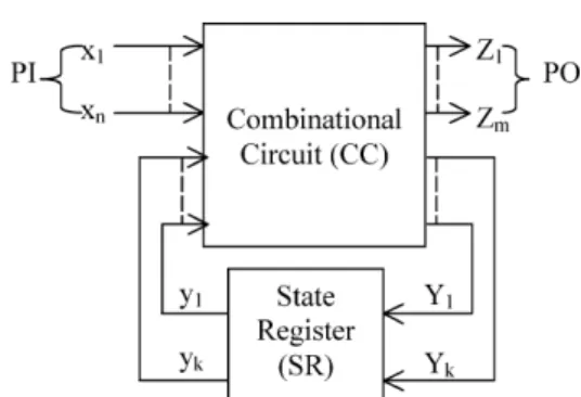
The general model of a synchronous sequential ma- chine (shown in Fig. 1) consists of a combina- tional circuit (CC) and a state register (SR) with n primary input (PI) x1,x2, . . . ,xn and m primary
Fig. 1. The general model of a sequential machine.
output (PO) Z1,Z2, . . . ,Zmlines. The outputs [inputs] y1,y2, . . . ,yk[Y1,Y2, . . . ,Yk] of k memory elements of SR define the present [next] state of the machine. We assume that the machine has a reset state. If a fault f in the sequential machine changes the transitions from a state Si, then to detect f , we have to first initial- ize the machine to state Si (called initialization state for f ) for which we need to apply a sequence of vectors known as justification sequence [4], to the machine in the reset state, which is to be followed by a differen- tiating sequence. A differentiating sequence [4] for a pair of states Sj and Sk, is a minimal length sequence of input vectors, such that the output response obtained by applying the sequence when the sequential machine is initially in Sj, is different from that obtained when it is initially in Sk. However, there may not exist any justification sequence for a state Si, as there may ex- ist some states in the machine that are unreachable or cannot be reached in sufficient time (hard to reach) from the reset state. Such a state is known as an invalid state, else it is a valid state. The list of invalid and valid states can be known from state transition graph (STG) of the machine. The combinational circuit of Fig. 2 ob- tained from the sequential machine of Fig. 1, by replac- ing inputs [outputs] of SR by pseudo primary outputs (PPOs) [pseudo primary inputs (PPIs)] is known as the
Fig. 2. CTGM of the machine of Fig. 1.
combinational test generation model (CTGM) of the machine.
3. New DFT Designs
From STG of the machine, we first find the set of valid and invalid states. Then a combinational ATPG tool is used to find the set of test vectors of the CTGM. Each such test vector is an ordered (n + k)-tuple, correspond- ing to n PIs and k PPIs. A state in a machine is called a test state, if it appears in PPI lines of any test vector of its CTGM. If a test state is a valid state (called as valid test state), then this state can be reached from the reset state. But if it is an invalid state (called as invalid test state), the value of PPIs cannot be set to the SR using state transitions. The problem of state initializa- tion to an invalid test state poses a major problem in test generation. This paper adopts a new technique to reach these states. Notice that to test a circuit, we need not reach all invalid states, reaching only to invalid test states are sufficient.
3.1. The First Technique
In our design, we append an extra logic called as CRIS to the original machine (shown in Fig. 3) to generate all invalid test states of the machine. CRIS has the inputs as the next state lines of the original machine. In a similar approach in [6], an additional circuit called ISG (invalid state generator) was also used to reach these invalid test states, where PIs are used as inputs to the extra logic.
(a) Designing CRIS. Let V [SITS] denotes the set of valid [invalid] test states of the machine. Then
Fig. 3. DFT to achieve complete fault efficiency (Technique 1).
any state Si ∈ V [SITS] can [cannot] appear in next state lines by proper [any] transition from reset state. CRIS makes also the appearance of SITS at the inputs to SR. For this, CRIS takes PPOs (Y1,Y2, . . . ,Yk) as the inputs, and produces (Y1′,Y2′, . . . ,Yk′) as inputs to SR using some con- trol inputs. The output of CRIS is the same as input when control inputs are at logic 0, and when one or more of them is 1, it produces some invalid test state. Optimization of number of control inputs and hardware of CRIS is an open problem. Here, we fol- low a heuristic approach. For each state Si∈ SITS, we first find how Sican be produced from each state Sj ∈V. For example, say an invalid test state 0101 can be produced from a valid state 0011 by comple- menting 2nd and 3rd bits of 0011. This can be done by using a control input C with C = 1 as shown in Fig. 4 (by ORing Y2 with C and ANDing Y3 with C¯). From each state Sj ∈ V, to reach Si, we get different possible productions. Among these differ- ent possibilities, we implement that with minimum hardware. If different invalid test states need com- plementation of same bit, we use the same control line. If any line requires both ANDing and ORing, we replace the gate by XOR.
(b) No. of control inputs and hardware overhead of CRIS. Theoretically, the number of such control lines can be maximum k, and that happens when there is only one valid state and there are at least 2k−1invalid test states. But practically, as number of invalid test states is much smaller (can be at most the number of test states) in comparison to total number (=2k) of states, and that is not very high in comparison to number of valid states, control lines requirement and hardware overhead cannot be high.
(c) Testing of CRIS. As all next state lines are observ- able, any fault in CRIS is also detected.
Fig. 4. An example of CRIS.
(d) Short test application time. When an initialization state Si for a fault is reached in present state lines of SR, hold mode is activated where the state of the machine is kept at Si, independently of the inputs at PIs. As several faults may have same test state Si, for all such faults test vectors are applied consec- utively holding the machine at state Si. Moreover, with the observation of next state lines, the length of differentiating sequence is always null. This ar- rangement highly reduces test application time. (e) Complete fault efficiency and short test generation
time.Use of CRIS and combinational ATPG tool make fault efficiency to be 100%. Test generation time is also reduced due to combinational ATPG.
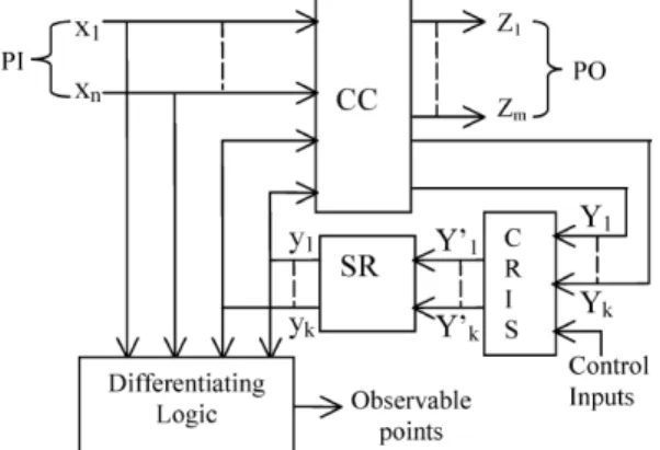
3.2. The Second Technique
The drawback of the first technique is its requirement of high number (=k) of additional observable points. To reduce it, we use one more additional circuit DL (Differentiating Logic) as shown in Fig. 5. Any fault in DL does not interfere with the original circuit behavior. (a) Design of DL. Two cases need to be considered.
Case 1. (k ≤ n) : In this case, the design of DL is as shown in Fig. 6 realizing one output, given by F = x1y1+¯x1¯y1+x2y2+¯x2¯y2+ · · · +xkyk+
¯xk¯yk. The function F has a unique property. For every combination of (y1,y2, . . . ,yk), yi ∈(0,1), the sub-function contains a unique pattern in xi’s, such that for a pattern (y1,y2, . . . ,yk) at PPIs, if we apply a pattern X at PIs with (x1,x2, . . . ,xk) = ( ¯y1,¯y2, . . . ,¯yk), we get the output of DL as 0, and
Fig. 5. DFT with complete fault efficiency and less observable pins (Technique 2).
Fig. 6. Differentiating logic (Case 1).
Fig. 7. K-map for k = 3 and n > 3.
for any other pattern at PI the output is at logic 1. It implies that if the machine reaches a state Si(y1,y2, . . . ,yk), then by applying a single in- put pattern, obtained by complementing each bit of (y, y2, . . . ,yk), this state can be uniquely identi- fied, i.e., differentiating sequence of any two states is of unit length.
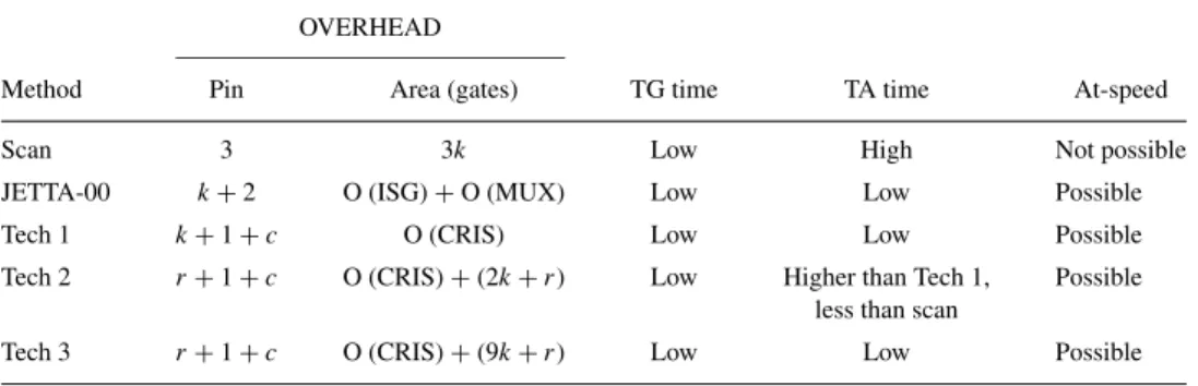
Table 1. Overall comparison.
OVERHEAD
Method Pin Area (gates) TG time TA time At-speed
Scan 3 3k Low High Not possible
JETTA-00 k +2 O (ISG) + O (MUX) Low Low Possible
Tech 1 k +1 + c O (CRIS) Low Low Possible
Tech 2 r +1 + c O (CRIS) + (2k + r ) Low Higher than Tech 1, Possible less than scan
Tech 3 r +1 + c O (CRIS) + (9k + r ) Low Low Possible
Fig. 8. Differentiating logic (Case 2).
Example 1. The K -map for k = 3 is shown in Fig. 7. Variables yi’s (xi’s) are used to label the map horizontally (vertically). A horizontal line in k-map corresponds to a state. Note that any state can be uniquely identified by a single input pattern. For ex- ample, state (y1,y2,y3) = (010), can be uniquely identified by the vector (x1,x2,x3) = (101). Case 2. (k > n): In this case, DL has r (= ⌈k/n⌉) outputs, and each output line of DL realizes Fi(1 ≤ i ≤ r) such that Fj +1 = x1yj n+1 + ¯x1¯yj n+1 + x2yj n+2 + ¯x2¯yj n+2 + · · · + xayj n+a + xayj n+a
where a = n for (0 ≤ j < r − 1), and a = k −(r − 1)n for j = r − 1. If a is found to be 1, then we replace Fj +1by yj n+1. The scheme is shown in Fig. 8.
(b) DL is universal. Design of DL is dependent on the number of PIs and flip-flops in the circuit, i.e., independent on the circuit structure.
(c) Use of hold mode. It is used to identify a state. If a state (y1,y2, . . . ,yk) is expected at present state lines, we activate hold mode and apply an input
for case 1 at PIs such that xi = ¯yi∀i(1 ≤ i ≤ k). For the case 2, we have to apply an input sequence instead of an input and in the sequence j (0 ≤ j ≤ r −1), xi = ¯yj n+i ∀i(1 ≤ i ≤ n). If the output [each output in case 2] of DL is 0, then the state of the machine is identified as the expected state.
(d) Low test application time. As differentiating se- quence is of length r = ⌈k/n⌉, test application time is greatly reduced, which is k in case of full scan per each test vector. To decrease it further, we adopt the following technique. Say to detect a fault, the machine is initialized to a state Si. Now, appli- cation of the test vector may change the state to Sj. If Sjis a test state, we use it as an initialization state of another fault. If Sjis not a test state, or there is no other fault to be detected with initialization state Sj, then we attempt to initialize the machine to any other test state.
(e) Testing of CRIS and DL. Any fault in DL or CRIS can be detected, by observing the output of DL. (f) Hardware overhead. It equals to (2k + r ) gates,
which is less than that of full scan for r < n − 1.
3.3. The Third Technique
Drawback of the second technique is that as observ- able points use present state lines, we cannot use the same justification sequence for different faults having same initialization state. To avoid this, in the third tech- nique, shown in Fig. 9, we use a register R to load the
Fig. 9. DFT design of Technique 3.
Table 2. STG characteristics.
Name #PIs #POs #States #FFs
bbara 4 2 10 4
bbsse 7 7 16 4
bbtas 2 2 6 3
beecount 3 4 7 3
cse 7 7 16 4
dk14 3 5 7 3
dk15 3 5 4 2
dk16 2 3 27 5
dk17 2 3 8 3
ex1 9 19 20 25
ex2 2 2 19 5
ex3 2 2 10 4
ex4 6 9 14 4
ex5 2 2 9 4
ex6 5 8 8 3
ex7 2 2 10 4
keyb 7 2 19 5
kirkman 12 6 16 4
lion 2 1 4 2
lion9 2 1 9 4
mc 3 5 4 2
opus 5 6 10 14
planet 7 19 48 6
planet1 7 19 48 6
pma 8 8 24 5
s1 8 6 20 5
s1488 8 19 48 6
s1494 8 19 48 6
s208 11 2 18 5
s27 4 1 6 3
s298 3 6 218 8
s386 7 7 13 4
s420 19 2 18 5
s510 19 7 47 6
s820 18 19 25 5
s832 18 19 25 5
sand 11 9 32 5
sse 7 7 16 4
styr 9 10 30 5
tav 4 4 4 2
tbk 6 3 32 5
tma 7 6 20 5
train11 2 1 11 4
train4 2 1 4 2
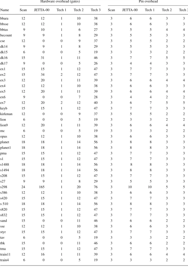
Table 3. Hardware overhead.
Hardware overhead (gates) Pin overhead
Name Scan JETTA-00 Tech 1 Tech 2 Tech 3 Scan JETTA-00 Tech 1 Tech 2 Tech 3
bbara 12 12 1 10 38 3 6 6 3 3
bbsse 12 12 1 10 38 3 6 6 3 3
bbtas 9 10 1 6 27 3 5 5 4 4
becount 9 9 1 8 29 3 5 5 3 3
cse 12 0 0 9 37 3 5 5 2 2
dk14 9 9 1 8 29 3 5 5 3 3
dk15 6 0 0 5 19 3 3 3 2 2
dk16 15 31 1 11 46 3 7 7 5 5
dk17 9 0 0 5 26 3 4 4 3 3
ex1 15 15 1 12 47 3 7 7 3 3
ex2 15 34 2 12 47 3 7 7 3 3
ex3 12 20 1 11 39 3 6 6 4 4
ex4 12 12 1 10 38 3 6 6 3 3
ex5 12 20 1 11 39 3 6 6 4 4
ex6 9 0 0 7 28 3 4 4 2 2
ex7 12 20 2 12 40 3 6 7 5 5
keyb 15 15 1 12 47 3 7 7 3 3
kirkman 12 0 0 9 37 3 5 5 2 2
lion 6 0 0 5 19 3 3 3 2 2
lion9 12 20 1 11 39 3 6 6 4 4
mc 6 0 0 5 19 3 3 3 2 2
opus 12 12 1 10 38 3 6 6 3 3
planet 18 18 1 14 56 3 8 8 3 3
planet1 18 18 1 14 56 3 8 8 3 3
pma 15 15 1 12 47 3 7 7 3 3
s1 15 15 1 12 47 3 7 7 3 3
s1488 18 18 1 14 56 3 8 8 3 3
s1494 18 18 1 14 56 3 8 8 3 3
s208 15 15 1 12 47 3 7 7 3 3
s27 9 9 1 8 29 3 5 5 3 3
s298 24 165 1 20 76 3 10 10 5 5
s386 12 12 1 10 38 3 6 6 3 3
s420 15 15 1 12 47 3 7 7 3 3
s 510 18 18 1 14 56 3 8 8 3 3
s820 15 15 1 12 47 3 7 7 3 3
s832 15 15 1 12 47 3 7 7 3 3
sand 15 0 0 11 46 3 6 6 2 2
sse 12 12 1 10 38 3 6 6 3 3
styr 15 15 1 12 47 3 7 7 3 3
tav 6 0 0 5 19 3 3 3 2 2
tbk 15 0 0 11 46 3 6 6 2 2
tma 15 15 1 12 47 3 7 7 3 3
train11 12 16 1 11 39 3 6 6 4 4
train4 6 0 0 5 19 3 3 3 2 2
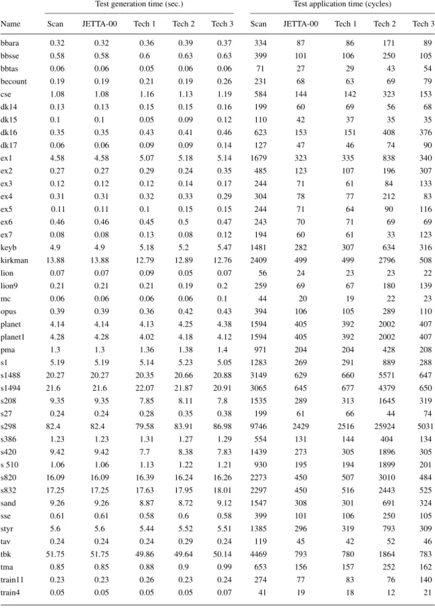
Table 4. Test generation /application time.
Test generation time (sec.) Test application time (cycles)
Name Scan JETTA-00 Tech 1 Tech 2 Tech 3 Scan JETTA-00 Tech 1 Tech 2 Tech 3
bbara 0.32 0.32 0.36 0.39 0.37 334 87 86 171 89
bbsse 0.58 0.58 0.6 0.63 0.63 399 101 106 250 105
bbtas 0.06 0.06 0.05 0.06 0.06 71 27 29 43 54
becount 0.19 0.19 0.21 0.19 0.26 231 68 63 69 79
cse 1.08 1.08 1.16 1.13 1.19 584 144 142 323 153
dk14 0.13 0.13 0.15 0.15 0.16 199 60 69 56 68
dk15 0.1 0.1 0.05 0.09 0.12 110 42 37 35 35
dk16 0.35 0.35 0.43 0.41 0.46 623 153 151 408 376
dk17 0.06 0.06 0.09 0.09 0.14 127 47 46 74 90
ex1 4.58 4.58 5.07 5.18 5.14 1679 323 335 838 340
ex2 0.27 0.27 0.29 0.24 0.35 485 123 107 196 307
ex3 0.12 0.12 0.12 0.14 0.17 244 71 61 84 133
ex4 0.31 0.31 0.32 0.33 0.29 304 78 77 212 83
ex5 0.11 0.11 0.1 0.15 0.15 244 71 64 90 116
ex6 0.46 0.46 0.45 0.5 0.47 243 70 71 69 69
ex7 0.08 0.08 0.13 0.08 0.12 194 60 61 33 123
keyb 4.9 4.9 5.18 5.2 5.47 1481 282 307 634 316
kirkman 13.88 13.88 12.79 12.89 12.76 2409 499 499 2796 508
lion 0.07 0.07 0.09 0.05 0.07 56 24 23 23 22
lion9 0.21 0.21 0.21 0.19 0.2 259 69 67 180 139
mc 0.06 0.06 0.06 0.06 0.1 44 20 19 22 23
opus 0.39 0.39 0.36 0.42 0.43 394 106 105 289 110
planet 4.14 4.14 4.13 4.25 4.38 1594 405 392 2002 407
planet1 4.28 4.28 4.02 4.18 4.12 1594 405 392 2002 407
pma 1.3 1.3 1.36 1.38 1.4 971 204 204 428 208
s1 5.19 5.19 5.14 5.23 5.05 1283 269 291 889 288
s1488 20.27 20.27 20.35 20.66 20.88 3149 629 660 5571 647
s1494 21.6 21.6 22.07 21.87 20.91 3065 645 677 4379 650
s208 9.35 9.35 7.85 8.11 7.8 1535 289 313 1645 319
s27 0.24 0.24 0.28 0.35 0.38 199 61 66 44 74
s298 82.4 82.4 79.58 83.91 86.98 9746 2429 2516 25924 5031
s386 1.23 1.23 1.31 1.27 1.29 554 131 144 404 134
s420 9.42 9.42 7.7 8.38 7.83 1439 273 305 1896 305
s 510 1.06 1.06 1.13 1.22 1.21 930 195 194 1899 201
s820 16.09 16.09 16.39 16.24 16.26 2273 450 507 3010 484
s832 17.25 17.25 17.63 17.95 18.01 2297 450 516 2443 525
sand 9.26 9.26 8.87 8.72 9.12 1547 308 301 691 324
sse 0.61 0.61 0.58 0.6 0.58 399 101 106 250 105
styr 5.6 5.6 5.44 5.52 5.51 1385 296 319 793 309
tav 0.24 0.24 0.24 0.29 0.24 119 45 42 52 46
tbk 51.75 51.75 49.86 49.64 50.14 4469 793 780 1864 783
tma 0.85 0.85 0.88 0.9 0.99 653 156 157 252 162
train11 0.23 0.23 0.26 0.23 0.24 274 77 83 76 140
train4 0.05 0.05 0.05 0.05 0.07 41 19 18 12 21
values of the next state lines and outputs of R are fed into DL. Use of hold mode is similar to that of the first technique.
4. Experimental Results
General performance of the DFT Design is described in Table 1. Rows “scan”, “JETTA-00”, “Tech 1”, “Tech 2” and “Tech 3” represent full scan, the method in [6], Technique-1, Technique-2 and Technique-3 re- spectively. O(ISG) and O(CRIS) indicate the over- head in gates of ISG (invalid state generator) in the paper of [6] and that of CRIS of this paper respec- tively. O(MUX) is the hardware overhead of multi- plexers used in [6]. It is found experimentally that O(CRIS) < O(ISG) + O(MUX). O(CRIS) was found to be maximum of two in MCNC benchmarks [9]. The value c is the number of control inputs needed for CRIS and r equals to ⌈k/n⌉, where n and k are respectively the number of PIs and flip-flops in the machine. In most cases of benchmarks, c is found to be 1, except in two cases, where it is found to be 2.
Experimental results on benchmarks are shown in Table 2. Autologic II (Mentor Graphics) tool synthe- sizes the circuits for MCNC benchmarks [9]. Columns
“name”, “#PIs”, “#POs”, “#states”, “#FFs” denote the name, the number of PIs, POs, states, and flip-flops of the original sequential machines respectively. We show only those cases when number of inputs (n) > 1. For n = 1, we apply only the first technique of our DFT designs.
Table 3 shows hardware and pin overhead. Hard- ware overhead of first technique is lowest and signifi- cantly small. Hardware overhead of both first and sec- ond techniques is smaller than that of full scan. The third technique needs more hardware as an additional register of k flip-flops are used. We have considered 7 gates per flip-flop in the third technique. Pin overhead of proposed second and third techniques are same and in most cases it equals to that of full scan which is always 3. The first technique requires more number of pins and it is same as that in method of [6]. Test generation and application time for different methods are shown in Table 4. A combinational/sequential test generation tool TestGen (Sunrise) is used. Results show that test generation time is almost equal in five cases. Test application time is almost equal in the method of [6], first technique and third technique and it is high- est in the case of full scan method. Second technique requires larger test application time in comparison to
those of first and third techniques, but this time is short in comparison to that of full scan.
5. Conclusions
The paper suggests three new techniques on non-scan DFT. As state initialization is a major problem in testing of sequential circuits, it solves that problem by using an additional hardware called as CRIS (circuit to reach invalid states). It is found experimentally that hard- ware overhead of CRIS is also low. The techniques use combinational ATPG tool to find the test sequences of the machine. Among the three techniques, hard- ware overhead of the first technique is lowest, but it requires k additional observable points. To decrease the number of observable points, a notion of differen- tiating logic (DL) is proposed in Technique 2. Even with the use of this DL, hardware overhead is less than that of full scan. Use of this DL increases test application time in comparison to that of first tech- nique, but this time is less than that of full scan. To achieve the test application time same as that of first technique, an additional register is used in third tech- nique. The novelty of these techniques is that they guar- antee complete fault efficiency with at-speed testing. Hardware overhead, test generation time and test ap- plication time compare favorably with those of earlier designs.
Acknowledgment
The authors would like to thank Drs. Toshimitsu Masuzawa, Tomoo Inoue, and Michiko Inoue for their helpful discussion.
Note
1. The ratio of number of faults detected or proved redundant by a test algorithm to the total number of faults in a circuit is known as fault efficiency.
References
1. S.T. Chakradhar, A. Balkrishnan, and V.D. Agrawal, “An Exact Algorithm for Selecting Partial Scan Flip Flops,” in Proc. of De- sign Automation Conference, 1994, pp. 81–86.
2. V. Chickermane, E.M. Rudnick, P. Banerjee, and J.H. Patel,
“Non-Scan Design-for-Testability Techniques for Sequential Cir- cuits,” in Proc. of Design Automation Conference, 1993, pp. 236– 241.
3. D.K. Das and B.B. Bhattacharya, “Testable Design of Non-Scan Sequential Circuits Using Extra Logic,” Proc. of Asian Test Sym- posium, 1995, pp. 176–182.
4. S. Devadas and K. Keutzer, “A Unified Approach to the Synthe- sis of Fully Testable Sequential Machines,” IEEE Transactions on Computer-Aided Design of Integrated Circuits and Systems, vol. 10, pp. 39–50, 1991.
5. H. Fujiwara, Logic Testing and Design for Testability, The MIT Press, 1985.
6. S. Ohtake, T. Masuzawa, and H. Fujiwara, “A Non- Scan Approach to DFT for Controllers Achieving 100% Fault Efficiency,” Journal of Electronic Testing: Theory and
Applications, pp. 553–566, 2000.
7. I. Pomeranz and S.M. Reddy, “Static Test Compaction for Full-Scan Circuits Based on Combinational Test Sets and Non-scan Sequential Test Sequences,” in Proc. of Int’l Conf. on VLSI Design, 2003, pp. 335– 340.
8. D. Xiang, S. Gu, and H. Fujiwara, “Non-Scan Design for Testa- bility Based on Fault Oriented Conflict Analysis,” Proc. of Asian Test Symposium, 2002, pp. 86–91.
9. S. Yang, “Logic Synthesis and Optimization Benchmarks User Guide,” Technical Report 1991-IWLS-UG Saeyang, Microelec- tronics Center of North Carolina.