Comput. Math. Applic. Vol. 13, No. 5/6, pp. 503-517, 1987 0097-4943/87 $3.00+0.00 Printed in Great Britain. All rights reserved Copyright © 1987 Pergamon Journals Ltd
A TESTABLE DESIGN OF PROGRAMMABLE
LOGIC ARRAYS WITH UNIVERSAL CONTROL
A N D MINIMAL OVERHEAD
K. K. SALUJA 1, H. FUJIWARA 2 and K. KINOSHITA 3
~Department of Electrical and Computer Engineering, University of Wisconsin-Madison, Madison, WI 53706, U.S.A.
2Department of Electronics and Communications, Meiji University, Kawasaki, 214 Japan
~Department of Information and Behavioral Sciences, Hiroshima University, Hiroshima, 730 Japan Abstract--In this paper we propose a new technique for designing easily testable PLAs. Our design is a hybrid of the many existing testable designs of PLAs and therefore has almost all features of existing designs. These are (1) simple design, (2) high fault coverage, (3) easiliy implemented on existing design automation systems, (4) little or no degradation of PLA performance in normal operations, and (5) elimination of need for test pattern generation and fault simulation. In addition to these, we define the silicon area overhead, g, associated with a PLA as an objective function. We then find a solution such that g is minimized in our design. Thus the additional feature our PLA possesses is (6) "minimal" overhead. The technique consists of addition of some bit lines as well as a shift register for control of product-lines during test mode. The extra logic is added in such a manner that all the easily testable features are maintained whereas the overall area of the extra logic is minimized. Using this design all multiple stuck-at faults, as well as all multiple extra and missing cross-point faults are detected.
1. I N T R O D U C T I O N
With the g r o w t h in the complexity o f V L S I circuits, the only w a y to carry out a circuit design to c o m p l e t i o n is by n o t only enlisting the help o f design a u t o m a t i o n ( D A ) tools but by m a k i n g use o f regular structures in the design process. A l t h o u g h , with the use o f D A tools almost any regular structure can be designed w i t h o u t m u c h difficulty, yet some regular structures have b e c o m e integral parts o f D A systems and o f integrated circuits (IC). M o s t c o m m o n l y used regular structures being R A M s , R O M s and P L A s ( p r o g r a m m a b l e logic arrays). Use o f P L A s in ICs is gaining increasing p o p u l a r i t y for the following reasons:
(1) It is a powerful structure to realized a r b i t r a r y c o m b i n a t i o n a l as well as sequential circuits. Therefore, its use reduces the overall complexity o f the chip design.
(2) P L A s can often be implemented as testable structures [1-11] thus m a k i n g the otherwise complex p r o b l e m o f testing V L S I circuits o f m a n a g e a b l e proportions.
(3) It is easy to include engineering design changes in ICs designed using PLAs.
(4) H a r d w a r e and silicon area required to implement a P L A can often be further reduced by using P L A minimization m e t h o d s [12-13].
In m o s t testable designs o f PLAs, e n h a n c e m e n t in testability is achieved t h r o u g h use o f additional logic to c o n t r o l individual p r o d u c t lines in test mode, t h o u g h some designs [17,18] are based on the ability to individually c o n t r o l bit lines. Typically, such a control over p r o d u c t lines is achieved by one o f the following two methods:
(1) Using a shift register (SR) or shift register with multiplexer [1,3-7]. (2) Using extra bit lines to f o r m a decoder or decoder like structure [2,8,9].
As both the m e t h o d s provide a l m o s t equal fault coverage, the superiority o f a m e t h o d depends on the a m o u n t o f silicon area overhead. B o z o r g u i - N e s b a t and McCluskey[9] argue that it is difficult to construct register cells with the same pitch as P L A pitch, thus a design e m p l o y i n g S R is likely to be inferior than a design which uses extra bit lines. O n the other h a n d H u a e t al.[7] and others [14] argue the use o f S R with multiplexers a n d SR with extra inputs or SR w r a p p e d a r o u n d a P L A to obtain a low silicon area overhead.
In general, d e p e n d i n g o n the function realized by a P L A , n u m b e r o f inputs, n u m b e r o f p r o d u c t lines and n u m b e r o f outputs; any o f the two m e t h o d s can result into a testable design with lower silicon area overhead.
503
504 K.K. SALUJA et al.
In this paper we marry the two approaches and show that the resulting design not only has the required fault coverage but results into an area overhead lower than the either approach.
This paper is organised as follows. In Section 2 of this paper we give preliminaries and describe the required notation and the details of the methods which are to be integrated in this paper. In Section 3 we propose the design of a universal control and discuss its properties. In Section 4 we described as to how partitioning can be employed to merge the universal control and the use of SR concepts. In Section 5 we find the optimal length of SR and size of control, analytically, such that overhead is minimized. Asymptotic bounds on overhead and further reduction of overhead for non-universal control are discussed in Sections 6 and 7, respectively.
2. P R E L I M I N A R I E S
In this section we present the notation and known testable designs. We also include some of the known results for the sake of completeness of this paper.
From logical description point of view, PLAs are two level sum-of-product realizations of combinational logic functions. Although in a given technology their implementation may not be AND/OR. For example nMOS PLAs are N O R - N O R implementations. However, for our analysis and presentation of results we choose A N D / O R realization. Conversion of the tests derived in this paper to suit N O R - N O R or other forms is a simple matter, Similarly, fault coverage results also apply to other forms of PLAs.
A general PLA structure is shown in Fig. 1. Input decoders, Dl, shown in this figure will be assumed to be one-bit decoders providing true and complement bit lines to the A N D plane. For simplicity of presentation other details of a PLA structure (e.g. pull-ups, grounds etc.) will now be shown. Program points of a PLA are intersection of bit lines and product lines in the AND-plane and product lines and output lines in the OR-plane. A PLA can be completely described by its personality matrices for A N D and OR planes. We shall denote the size of a PLA by an ordered triple (n, m, l) having n = number of inputs, m = number of product lines and / = number of
x I
x 2
X n
. D I
&>
PI P2 Pm
- j
-- " ' f 2
L
\OR Plane Fig. 1. A general PLA structure.
AND Plane
fg,
A testable design of programmable logic arrays 505
Extra ~ Additional Logic to
Control__Inputs Control product lines (L~
• • • • • , • o . • o
0=
O
~ AND plane
l • • • • o • • • • • •
Decoder
OR
p l a n ei
O
e~
o
~ a
Q
" ] Additional Logic in OR plane (L R)
Fig. 2. A general structure of testable PLAs.
I Exit;
Observable
Outputs
outputs. The personality matrix A for AND plane is an n x m matrix whose entries are defined as follows:
1 if ith input a n d j t h product line have a cross-point present
ai.j = 0 if complement of ith input and j t h product line have a cross-point present
- otherwise.
Similarly, the personality matrix Q for the OR plane is a l x m matrix whose entries are as follows:
f 1 if ith output and j t h product line have qu = a cross-point present
- otherwise.
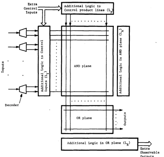
Typically, all testable designs incorporate extra logic to enhance testability. A general structure of a testable PLA is shown in Fig. 2. While discussing different testable design we shall often refer to this figure.
2.1. F a u l t m o d e l
We shall assume that only the following faults can be present in a PLA: (1) any number of s-a faults; (2) any number of extra devices; and (3) any number of missing devices.
506 K.K. SALUJA et al.
T h o u g h we do not assume the presence of adjacent line bridging faults, yet they can be detected with only a minor modifications in some of the cases discussed in this paper. Also, as Saluja et al.[11] have shown that s-a faults in a P L A are equivalent to missing device or output s - a - 0 faults, therefore, while presenting the proofs we shall only consider the fault set modified accordingly. 2.2. Bozorgui-Nesbat and McCluskey's (BM) approach [9]
In this approach Lp (Fig. 2) consists of a decoder-like structure. Extra inputs are added such that the resulting A matrix has certain distance properties. LI essentially consists of a circuit which can be enabled only during test m o d e (in n M O S it will consist of pull down transistors on extra lines). We shall call the P L A obtained with this approach a BM-PLA. In our notation, Pi denotes ith product line as well as function realized by ith product line. An n-bit input vector will be denoted as X = (c~, c2 . . . c,).
DEFINITION 1
A set of inputs, S,, is called a select set of Pg if Si = {X/Pg(X) = 1 }. DEFINITION 2
An input vector t~.0 is called main test pattern of Pj if (1) t~,0~S i and (2) dn(t~.o,X) i> 2 for all X and Sj such that X~Sj and j # i, where dH(a, b) is H a m m i n g distance between vectors a and b. DEFINITION 3
For a main test pattern tl,0 = (c~, c2 . . . c,) for Pg we define n auxiliary test patterns of P~ as tij=(c2,c2 . . . cj l, ?j, Cj+l . . . c , ) ; j = 1,2 . . . n
DEFINITION 4
Test patterns for Pi, TP,, is the set defined as: TP~ = {tg.0, ti, L .. . . . t~,,}. DEFINITION 5
Test set for BM-PLA, TBM is defined as TBM = TP1 U TP2 U • • - t_J TPm. THEOREM 1 [9]
A B M - P L A can be tested for all faults by the test set TBM.
In [9] is given a procedure for adding extra inputs such that the resulting P L A is easily testable. N u m b e r of extra inputs depend on the A matrix of the original PLA. Computational complexity of the procedure which changes a P L A to B M - P L A is 0(m3).
2.3. Khakbaz's (K) approach [5]
In this a p p r o a c h Lp consists of a SR to control the individual product lines. N o extra logic is required at L~. An extra observable output is added. We shall call the P L A obtained by this approach a K-PLA. In deriving the tests for K - P L A , a test vector will be denoted by a (m + n)-bit vector, (rl, r2 . . . rm; c~ . . . c,). The first m bits denote the contents of SR, and the remaining n bits indicate the inputs. We shall often group them together and denote the test vector as (R, X). The following R and X vectors are o f special interest for deriving tests for K-PLA.
DEFINITION 6
Vectors R 0 and R~ are defined as follows:
R0 = (0, 0
. . . 0)R~= (0,0 ... 0,1,0 ... 0).
DEFINITION 7
An input Xi is called a test input for Pi if Xi ~ & (see definition 1 for S,). DEFINITION 8
If X~ (test input for P~) is denoted as (c~, c2 . . . c,), we define n auxiliary test inputs for P~ as Xi,j = (cl, c2 . . . ?j . . . on); j = 1, 2 . . . n.
A testable design of programmable logic arrays Table I. Comparison of different testable designs
BM-PLA K-PLA SKF-PLA and F-PLA
Extra logic Lp
(1) Type Decoder like SR SR
(2) Dependence
on PLA Yes No No
(3) Extra inputs f(PLA) 1 I
(4) Computation
complexity 0(m 3) Nil Nil
(5) Cost f(PLA) f(m) f(m)
Extra logic LI
(1) Type Controllable Nil SR/gates
extra inputs (2) Delay
inserted Nil Nil Y e s
(3) Cost Constant Nil f(n)
Test generation
(1) Required Yes Yes No
(2) Length f(n, m) f(n, m) f(n, m)
(3) Fault s-a and s-a and s-a, cross-
Coverage cross-points cross-points points and
bridging (4) Stored test
patterns m m Constant (2)
f(x, yl...) means a function of x, y, etc; f(PLA) means a function of personality of PLA.
507
DEFINITION 9
Test vectors for ei, TVi, is the set TV~ = {(Rj; X~), (R~; Xi, j), (Ri; X;,2), • • •, (R~, Xt,.)}. DEFINITION 10
Test set for K-PLA, TK, is defined as
TK = TV0 t_J T V 1 [3 T V 2 I.J • • • ~ 1 T V m ,
where
TVo = {(Ro; X~), (Ro; X2) . . . (Ro; Xm)}. THEOREM 2 [5]
A K - P L A can be tested for all faults b y the test set TK. 2.4. Saluja et al.[4] (SKF) and Fujiwara[6] (F) approaches
In these a p p r o a c h e s L o consists o f a S R to c o n t r o l the i n d i v i d u a l p r o d u c t lines. L~ consists o f a d d i t i o n a l c o n t r o l l a b l e logic in the f o r m o f S R [4] o r gates [6] to p r o v i d e i n p u t s to the A N D p l a n e o f the P L A such t h a t the resulting P L A can be tested by test sets i n d e p e n d e n t o f the p e r s o n a l i t y o f a P L A . W e d o n o t d e s c r i b e the necessary test sets here, as it will m a k e this p a p e r u n d u l y long. H o w e v e r , the f o l l o w i n g t h e o r e m is a c o n s e q u e n c e o f these works. In a l a t e r section in this p a p e r we will a p p l y the key idea used in S K F - P L A a n d F - P L A to arrive at a new design.
THEOREM 3[4,6]
S K F - P L A a n d F - P L A can be tested for all faults by test sets i n d e p e n d e n t o f the P L A . F u r t h e r m o r e , S K F - P L A a n d F - P L A can also be tested for a d j a c e n t line b r i d g i n g faults. 2.5. Comparison
C o m p a r a t i v e a d v a n t a g e s a n d d i s a d v a n t a g e s o f the different designs discussed a b o v e a r e listed in T a b l e 1.
3. U N I V E R S A L C O N T R O L
In this section we p r o p o s e a design o f Lp which m a k e s use o f e x t r a i n p u t s a n d bit lines s i m i l a r to B M - P L A s . H o w e v e r , the design p r o p o s e d will be universal in n a t u r e , i.e. i n d e p e n d e n t o f the p e r s o n a l i t y o f P L A . T h e a l g o r i t h m d e s c r i b e d in [9] for a d d i n g e x t r a i n p u t s to the P L A has a
508 K.K. SALUJA et al.
computational complexity of
0(m3).
For large PLAs, use of such an algorithm can be prohibitively expensive, thus making the use of this method applicable only to small PLAs.We shall first study some properties of a special AND-array, called a decoder-parity- AND--array (DPAA), defined below.
DEFINITION 11
A D P A A is an A N D - A r r a y with m product lines, [-log: m 7 + 1 inputs and with the A matrix AD as follows: if m columns o f AD matrix are numbered from A0 to A,,_ t, and
- al,i i a2,i
i "
A i
I
an, i! a
L n+ I.i_
then (a.,t . . . a2,t, al,,) is the binary representation of i and a.+ta = a.,t ~ " • • • a2,i (~ al,g. The following lemmas describe some properties of a DPAA.
LEMMA 1
dH(At, Aj)>~2; O<~i, j < m ; i : ~ j . LEMMA 2t
For the DPAA, the select set 5',. of Pi is uniquely determined and consists of a single pattern. Notationally, ISil = 1 and St = AT.
The following definition is a minor variation of the definition in [9] and is stated here for the sake of completeness of this paper:
DEFINITION 12
The distance matrix, D, of a PLA is a m × m matrix whose entries are defined as follows: D i . s = m i n { d n ( X , Y ) l X ~ S t , Y E S j } ; i ~ j
---2 for i = j . LEMMA 3
Every element of the distance matrix for the D P A A is greater than or equal to 2. P r o o f It follows from Lemmas 1 and 2. []
DESIGN 1
Augment a given (n, m, l) PLA by concatinating a DPAA to it as shown in Fig. 3b. We shall call this PLA as D I - P L A . In Fig. 3 we have not shown the extra logic which can be used to disable the DPAA part of the PLA during normal operation of the PLA. In nMOS PLAs [16] such a circuit will be of the form shown in Fig. 3c. Note that k = I-log 2 m ] and total number of extra inputs to D1-PLA are (1 + k). We now derive a test set for D1-PLA.
Let Si be the select set of P~ for the original PLA. Let {ut} by the select set of P~ for the decoder-parity PLA. Then, the select set of Pt for the augmented PLA is
at.st
= {(u,,X)lX s,}. LEMMA 4For all X e Si and V 6 S/, dx [(u+, X), (u/, Y)] >/2.
This lemma guarantees that any element of the select set of Pt for the augmented PLA can be a main test pattern of Pi.
tlx] means cardinality of a set x; yr means transpose of a vector Y.
A testable design of programmable logic arrays 509
AND
Array
OR
Array
(a) Original PLA.
d . 1
f 1
dl .
d k •
d k
Xl ~
X n
Decoder-
Parity
[ . . . I
AND
Array
I * •1 ° • ° • • I
OR Array
I
(b) Augmented PLA.
(c) Extra transistors on inputs Fig. 3. Testable
e
1
of DPAA in the case of nMOS realization. design of a PLA (DI-PLA).
! f l
f~
Let ti. 0 be any one of the elements of ui" 3",.. For a t~, o, we can obtain the auxiliary test patterns of P~. Let these be ti, l,t~,2,..., ti.~+ F~og2m~ +,.
Then, the test patterns for the D1-PLA are: TDI = {tl,o, tj,l . . . tl,~+ flog2,,,] +l,
t2,0, t2,1 . . . . , t2,n+ rlog2,~] +1, tm, o, tm, t . . . . , t,,,~+ Flo~2,~l +l}" THEOREM 4
The D I - P L A of Fig. 3b can be tested for all faults by the test set TD~ mentioned above. Proof. It follows from Theorem 1 and Lemma 4.
THEOREM 5
The length of the test set to test D1-PLA is m(2 + n + log2 m). All these test patterns can be generated from m main test patterns.
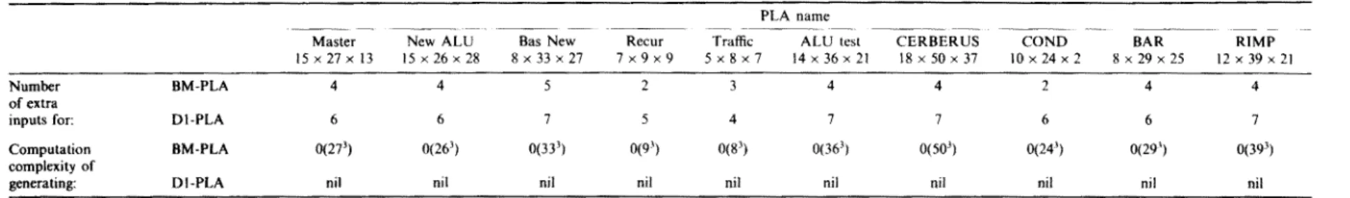
Comparison of this method with BM-PLA is given in Table 2 for 10 PLAs taken from [9]. The number of extra inputs in D 1 - P L A is not much larger than BM-PLA, but the computational complexity for generating D1-PLA is nil. Minimization of overhead (number of inputs as well as silicon area) with the use of D P A A is the subject of the next two sections.
4. P A R T I T I O N I N G
In this section we propose a partitioning procedure which helps reduce the number of extra inputs without sacrificing the testability properties of the PLA. The basic idea being a PLA is partitioned into k blocks, each block containing m / k product lines. A D P A A is appended to each
Table 2. Comparison of BM-PLA and DI-PLA PLA name
Master New ALU Bas New Recur Traffic ALU test CERBERUS COND BAR R1MP
5 x 2 7 x 1 3 15 x 2 6 x 2 8 8 x 3 3 x 2 7 7 x 9 x 9 5 x 8 x 7 1 4 x 3 6 x 2 1 1 8 x 5 0 x 3 7 1 0 x 2 4 × 2 8 x 2 9 x 2 5 1 2 x 3 9 x 2 1
,lumber BM-PLA 4 4 5 2 3 4 4 2 4 4
~f extra
aputs for: DI-PLA 6 6 7 5 4 7 7 6 6 7
~omputation BM-PLA 0(273 ) 0(263 ) 0(333 ) 0(93 ) 0(83 ) 0(363 ) 0(503 ) 0(243 ) 0(293 ) 0(393 )
omplexity of
',enerating: DI-PLA nil nil nil nil nil nil nit nil nit nit
. +
l og
L 2
~lock i Block 2
k
DPAA
AND Array
OR
Array "~
51ock k
?'ig. 4. P a r t i t i o n i n g o f a P L A ( D 2 - P L A ) .
A testable design of programmable logic arrays 511
block as shown in Fig. 4. Furthermore, an SR of length k is introduced to control these blocks. The formal design description and the testability properties of the resulting PLA are given below. DESIGN 2
Product lines of a PLA are divided into k blocks with each block containing h product lines, i.e. h = [ m / k ] . Note that all but the kth block have h product lines, where as number of product lines in the kth block are m - ( k - l)h. A DPAA is appended to each block. All DPAAs receive the same inputs thus total number of extra inputs to the PLA are 1 + [-log2h-]. An SR of length k is appended. The resulting PLA is called D2-PLA (Fig. 4).
While discussing testing of D2-PLA we must not lose sight of the actual realization and physical failures. Keeping this in mind we make the following observations.
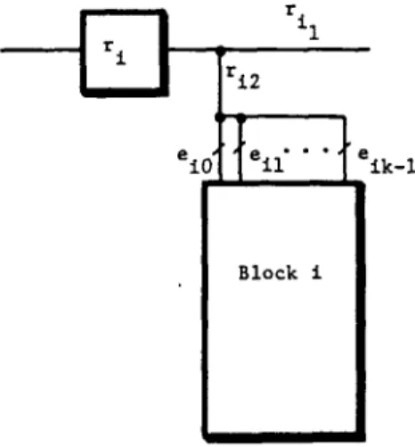
OBSERVATION 1
Saluja et al.[ll] have shown that in a PLA all s-a faults can be reduced to multiple missing cross-point or outputs s-a-0 faults. However, s-a-1 faults at ri~, ri 2, e~ 0, ei, . . . etc, for block i shown in Fig. 5 must be tested explicitly. Although s-a-l-faults at these locations will not interfere in the normal operation of a PLA yet their presence may invalidate other tests. Thus our fault set is (1) multiple cross-points (extra and/or missing) and output(s) s-a-0 faults and (2) s-a-1 faults at location marked in Fig. 5. Notice that this fault set includes the fault set given in Section 2.1. OBSERVATION 2
In Fig. 4, the number of extra inputs is (1) 1 for SR and (2) 1 + [log: h 7 for DPAAs. However, if we take h = 1 then Design 2 should be degenerated to K-PLA requiring no DPAA. Similarly, for h = m Design 2 should be degenerated to D 1 - P L A requiring no SR.
Further, in the presence of SR we would need to observe the output rk, to test SR. OBSERVATION 3
We can introduce an extra output, z*, in the OR-plane similar to [4-6], in which case the A N D plane can be completely tested by observing only z*. However, to test the OR-plane, as well as outputs s-a-0, all outputs need to be observed, therefore it is not necessary to introduce z* outputs and complete testing can be carried through by observing the normal outputs of D2-PLA.
We now describe the testing of D2-PLA. Testing is carried in a number of conceptual steps described below, though in practice these steps can be merged to obtain a reduced test set.
Step 1: Testing SR. SR is tested by applying a sequence of zeros, followed by a one, followed by zeros and observing the rk, output. This will also detect s-a faults at r~,s in any block.
Step 2: Testing s-a- 1 faults at locations marked in Fig. 5. Set rt = r, . . . rk = 0. Now apply m main test patterns. All outputs must stay zero during this test for a fault free PLA.
eio{{ ell" " " t
eik- IBlock i
Fig. 5. Certain fault sites in block i.
512 K.K. SALUJA et al.
Step 3: Testing P L A . Each block of the P L A is now tested independently. To test block i set r e = 1 and % = 0 for j # i. Apply h (2 + n + I-log 2 h 7) test patterns required to test block i.
This completes the testing procedure.
The following theorem states this result formally though the p r o o f has not been included as it is straightforward.
THEOREM 6
The D2-PLA of Fig. 4 can be tested for all faults by tests stated in above three steps. THEOREM 7
The length of the test set to test D2-PLA is m(3 + n + I - l o g 2 h q).
Proof. This is total n u m b e r of tests in Steps 2 and 3 above. Test for SR is included in these steps. []
5. O P T I M A L P A R T I T I O N I N G
In the previous section we discussed how using partitioning one can reduce the number of extra inputs without sacrificing the fault coverage. O f course, if reduction of number o f extra inputs is the only objective than S K F - P L A , F - P L A or K - P L A are optimal (in general) by choosing h = 1. Here we set out objective as follows:
Objective: Find optimal partitioning such that the area of Lp in D 2 - P L A is minimized. Notice that in D 2 - P L A the only added logic is in the form of Lp (other than disabling transistors for extra inputs--these are not shown in the figure to keep the figure simple). Therefore, minimizing the areas of Lp will result in a minimal overhead PLA.
We now define the cost function. Let w~ be the area of a PLA cell and w2 to be the area of a SR ceil.
It is difficult, if not impossible, to have the pitch of SR cells the same as PLA pitch. However, in D 2 - P L A we need the pitch of SR cells to be h x PLA pitch, to avoid any interconnection overheads. In the following discussion we assume such to be the case, i.e. h will be large enough to make interconnection overhead as zero. Notice interconnection overhead can also be reduced to zero by having SR wrap around P L A [14] or by use of SR with multiplexers [7].
In a D 2 - P L A increase in area of P L A by adding an extra bit line is mwj. Therefore an extra input increases the area of P L A by 2mw~. Thus in D2-PLA the overhead
g = 2 m w ~ ( l + V l o g 2 h T ) + k w 2 (1) where
k = [ m / h
]
.Our objective is to find h = t i m , w~, w2) such that g is minimized.
Note: (i) There are two special cases which are not included in equation (1) to keep the presentation simple. These are (a) for h = 1, g = mw2; (b) for h = m, g = 2mw~(1 + ['log2m'] ). (ii) The solution for h must be found in the set of integers.
The following theorem simplifies the solution space for h considerably. Tr~OREM 8
I f g is minimized for some h such that 2' ~ < h < 2' then g is also minimized for h = 2". Proof. I f g is minimized for 2 '-~ < h < 2' then
gmin=2mwl(l + : x ) + Fro~hi w 2
g h = 2 ' = 2mw~ (1 + ~) + [m/2"-] w 2 but
therefore
[m/2~7 <~ [ m / h ' ] for h < 2"
gh=2, ~< groin
A t e s t a b l e design o f p r o g r a m m a b l e logic a r r a y s 513
but g.~, is minimum, therefore
g h = 2 • = gmin" [ ]
The implication of Theorem 8 is that while finding the minimum value ofg we need only consider those h which are some powers of 2. Therefore a solution can easily be found either by hand computations or by using computer. The problem can also be solved analytically by solving the equation
dg
- - = 0 . ( 2 )
dh
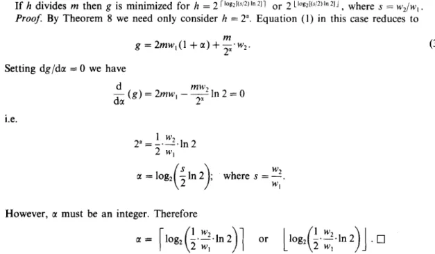
To gain some insight into the solution method we first consider the case where 2~( = h) divides m. Note a sufficient conditions for this case is m to be a power of two.
THEOREM 9
If h divides m then g is minimized for h = 2 [-I°g2[(s/2)ln2]] or 2 Ll°g2[(s/2)ln2]] , where s = w J w , . P r o o f . By Theorem 8 we need only consider h = 2 ~. Equation (1) in this case reduces to
g =2mwl(1 + c t ) + - ~ ' w 2. m
Setting dg/do~ = 0 we have d
d~ ( g ) = 2row, - -
i.e.
m w 2
~ - l n 2 = 0
2~ " = ~ ' ~ ' m 2 1 w2,
(;)
-e = l o g 2 In2 ; w h e r e s = - -
w!
(3)
However, ~ must be an integer. Therefore
~ = [log2 (~. w~-ln 2) 1 or ~logl(~' w~.ln 2) J . F-1
The general solution is not as straightforward and leads to a recursive but approximate relation given by the following theorem:
THEOREM 10
g is minimized when
where
L ( sm' )1 r l.m )l
h = 2 log2 ~ ' - ~ l n 2 or 2 Ll°g2{k2mln2
S = - - ; W2 W1
m = q h + 7 = m l + 7 ; 0 ~ 7 < h .
Table 3. Optimal value of ~t for different m and s m
s 16 20 30 32 40 50 60 64 70 80 90 100 128
10 2 2 2 2 2 2 2 2 2 2 2 2 2
20 4 ~ 3 3 3 3 3 3 3 3 3 3 3
30 4 3 ~ 3 3 3 ¼ 3 3 3 ~ 3 3
514 K.K. SALUJA et al. Proof. P r o o f is similar to the proof for Theorem 9. We set
F:I m,
= = + l = T + l
and h = 2 ~ (by Theorem 8) in the expression for g and set dg/d~ = O. []
Note that although Theorem 10 gives a recursive solution it is very easy to solve by successive approximation by first approximating the value of h using the result of Theorem 9 and then making a correction in the solution. The solution never takes more than 2 steps of approximations. It is interesting to note that the solution is almost independent of m and depends only on s, i.e. the ratio (area of SR cell)/(area of PLA cell).
Table 3 gives values of ~ for different values of m and s. It is, evident from this table that BM-PLA are only likely to be optimal for small PLAs and for large s. In other conditions partitioning is likely to provide lower overhead. We don't know the ratio s for the layout of PLA used in [7], but we conjecture that s was approx. 10 and therefore, instead of one-bit multiplexer, the use of a two-bit multiplexer would have resulted in a PLA with still lower overhead.
6. A S Y M P T O T I C O V E R H E A D
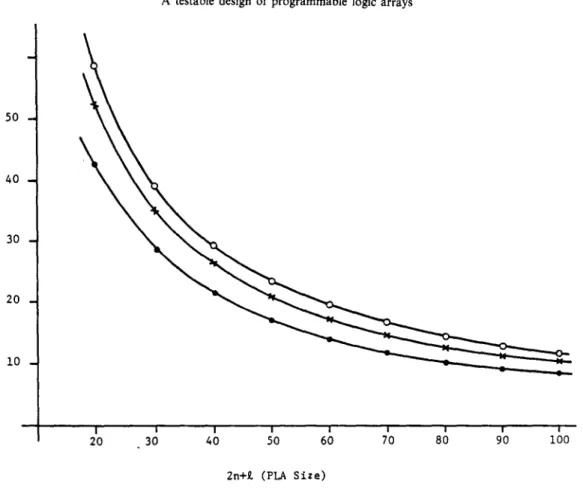
In this section we derive simplified expression of overhead for large PLAs. The total area of an nMOS PLA is given by area of A N D / O R planes and area of input inverters, pull-ups, etc. For derivation of simple expression we shall consider only the area of A N D / O R planes, i.e. PLA area = m(2n + l)wl.
In D2-PLA, the area of extra logic
If we simplify V m/2"-] gmin as m/2 ~
g =
% overhead = Therefore
2m(1 + ~ ) w I + Vm/2~7 w2. then the extra area
m 2 ( 1 + = ) + w..
100m 2 ( 1 + ~ ) + wl m(2n + l)wl
100(2(1 + ~ ) + ~ )
2n + l (4)
From Table 3 we observe that ~ is 2, 3 and 3 for values of s of 10, 20 and 30 respectively for large m. On substitution of these values of ~ and s in (4) we obtain
s = 10; % o v e r h e a d = - - 850 2n + I
1050 s = 2 0 ; % o v e r h e a d = - -
2n + 1 1175 s = 3 0 ; % o v e r h e a d = 2 n + l .
These values are plotted in Fig. 6. Note that the above expressions are on the conservative side as the actual area of original PLA will be more than the area of A N D / O R planes only. Thus percentage overhead in practice is likely to be less than the above bounds.
7. F U R T H E R R E D U C T I O N IN O V E R H E A D
In the previous sections we have described a way of reducing the overhead through the use of a DPAA. However, the basic reason a D P A A was appended to each block of Fig. 4 was that each
A testable design of programmable logic arrays 515
so -.
4 0
30 -
2 0 -
i 0 -
I i I I I I i • i
20 30 4 0 50 60 70 80 90 i00
2n+~ (PLA Size)
Fig. 6. Percentage overhead for D2-PLAs.
element o f the distance matrix for each block should be no less than 2. We now propose an alternate design and discuss some of its properties.
DESIGN 3
The product lines o f a PLA are divided into k blocks. For a block i n u m b e r o f extra inputs, ei, and cross points are determined by using the algorithm given by Bozorgui-Nesbat and McCluskey[9]. N o w each block of the PLA has desired distance property, the extra inputs are connected together along with an SR of length k, as shown in Fig. 7. We call this design a D3-PLA. The total n u m b e r of extra inputs to D 3 - P L A are e = max{ej, e 2 . . . ek}.
A D 3 - P L A can be tested in the same m a n n e r as a D2-PLA. We therefore can state the following theorem based on Theorems 6 and 7:
THEOREM 11
The D 3 - P L A o f Fig. 7 can be tested for all faults by a test set o f length m(2 + n + e). To show as to how D 3 - P L A can result into an overhead lower than D2-PLA as well as B M - P L A we consider a simple example.
Let us consider C E R B E R U S PLA [9]. It is a 18 x 50 x 37 PLA. It is evident that D 3 - P L A can be no worse than D2-PLA because if we find that the n u m b e r o f extra inputs for any block are larger than 1 + ~-log2 h ] , we can realize such a block by appending a DPAA.
To show that we can actually improve on B M - P L A we note the following fact: FACT 1
e ~< n u m b e r o f extra inputs for BM-PLA.
N o w let us say we divide the 50 lines of C E R B E R U S P L A into 4 blocks for realization of D3-PLA. It can be expected that the n u m b e r o f extra inputs will reduce by at least 1, i.e. from 4 for B M - P L A to 3 in D3-PLA, whereas an SR o f length 4 will be added.
516 K.K. SALUJA et al.
1 + rlo~ ~-I
i
°, ... ] D P A AB M - P L A 2
n
I I
[
° . . w
' i I
I I I I ]
i ....
O R O R
A r r a y • A r r a y . . . .
B l o c k I B l o c k 2
k
Fig. 7. A D3-PLA.
i-
IT ... DPAA
,M-PLA
!
O R
I ! z
Array .
B l o c k k
Thus the total change in the area from the B M - P L A is K = - 2 × 50 × w, + 4 w 2
= - 100wl + 4w2
This change is negative as long as s < 25. In general for large PLAs we can expect a larger reduction in the n u m b e r of extra inputs while changing a B M - P L A into D3-PLA.
Similar arguments hold for other larger examples in [9]. An additional benefit in adopting D 3 - P L A over B M - P L A is reduced computational complexity which is stated in the form of the following lemma.
LEMMA 5
Computational complexity to generate D3-PL is O(m3/k 2) as opposed to 0(m 3) for BM-PLA. 8. C O N C L U S I O N
In this paper we have proposed three testable designs of PLAs. These designs can be seen as methodologies to improve over the existing designs. We have set different goals at different stages of the design. While moving from D 1 - P L A to D 2 - P L A we retained all the properties of D1-PLAs yet reduced and overhead. While introducing D3-PLA, again we were able to reduce the overhead, complexity of generation of PLA, still maintaining the fault coverage. It is simple to incorporate m a n y other variations of these designs, For example, it is possible to design PLAs which are testable by a universal test set and use the partitioning and distance concept to reduce overhead. Such a P L A is discussed in [15].
The methods proposed in this paper are straightforward to incorporate in design automation systems. In this paper we have also described how a n u m b e r of designs can be merged to give rise to a design superior than the all known designs in the case of PLAs. These concepts can be included in expert systems and m a y possibly result into still improved designs and design methodologies.
R E F E R E N C E S
1. H. Fujiwara and K. Kinoshita, A design of programmable logic arrays with universal tests. IEEE Trans. Comput. C30, 823-828; also IEEE Trans. Circuits Syst. CAS28, 1027-1032 (1981).
2. S. J. I-long and D. L. Ostapko, FITPLA: A programmable logic array for function-independent testing. Digest, lOth Int. Symp. Fault-Tolerant Computing, pp. 131-136 (1980).
3. S. Yajima and T. Aramaki, Autonomously testable programmable logic array. Digest, llth Int. Syrup. Fault-To&rant Computing, pp. 41-43 (1981).
4. K. K. Saluja, K. Kinoshita and H. Fujiwara, An easily testable design of programmable logic arrays for multiple faults. IEEE Trans. Comput. C32, 1038-1046 (1983).
A testable design of programmable logic arrays 517
5. J. Khakbaz, A testable PLA design with low overhead and high fault coverage. IEEE Trans. Comput. C33, 743-745 (1984).
6. H. Fujiwara, A new PLA design for universal testability. IEEE Trans. Comput. C33, 745-750 (1984).
7. K. A. Hua, J. Y. Jou and J. A. Abraham, Built-in tests for VLSI finite-state machines. Proc. 14th Int. Syrup. Fault-Tolerant Computing, pp. 292-297 (1984).
8. T. Sato and Y. Tohma, A new configuration of PLA with function independent tests. Technical Report, Department of Computer Science, Tokyo Institute of Technology, Tokyo, Japan (1982).
9. S. Bozorgui-Nesbat and E. J. McCluskey, Lower overhead design for testability of programmable logic arrays. Proc. 1984 Int. Test Conf., pp. 856-865 (1984).
10. Y. Min, A PLA design for ease of test generation. Proc. 14th Int. Syrup. Fault-Tolerant Computing, pp. 436-442 (1984). I 1. K. K. Saluja, K. Kinoshita and C. Boswell, A design of parallel testable programmable logic arrays. Proc. Int. syrup.
Circuits and Systems, pp. 1325-1328 (1985).
12. G. D. Hachtel, A. R. Newton and A. L. Sangiovanny-Vincentelli, An algorithm for optimal PLA folding. IEEE Trans. CAD Integrated Circuits Syst. CAD1, 63-77 (1982).
13. R. H. Mak, Optimization of programmable logic arrays. Integration 2, 149-162 (1984).
14. C. Boswell, A comparative study of testable design of programmable logic arrays. M. E. Thesis, University of Newcastle, N.S.W., Australia (1986).
15. K. K. Saluja and J. S. Upadhaya, Divide and conquer strategy for testable design of programmable logic arrays. 4th Aust. Microelectronics Conf. Sydney, pp. 121-127 (1985).
16. C. Mead and L. Conway, Introduction to VLSI Systems. Addison-Wesley, Reading, MA (1980). 17. J. Rajski and J. Tyszer, Easily testable PLA design. Euromicro 139 146 (1984).
18. J. Rajski and V. K. Agarwal, Testing properties and applications of inverter-free PLAs. Proc. 1985 Int. Test Conf., pp. 501~507 (1985).
20. K. S. Ramanatha and N. N. Biswas, A design for testability of undetectable crosspoint faults in programmable logic arrays. IEEE Trans. Comput. C32, 551-557 (1983).
21. H. Fukiwara, Logic Testing and Design for Testability. MIT Press, London (1985).
C.A.M.W.A. 13/5-6--H