Rev. 6 — 4 April 2014
User manual
Document information
Info Content
Keywords I2C, I2C-bus, Standard-mode, Fast-mode, Fast-mode Plus, Fm+, Ultra Fast-mode, UFm, High Speed, Hs, inter-IC, SDA, SCL, USDA, USCL
Abstract Philips Semiconductors (now NXP Semiconductors) developed a simple bidirectional 2-wire bus for efficient inter-IC control. This bus is called the Inter-IC or I2C-bus. Only two bus lines are required: a serial data line
Contact information
For more information, please visit: http://www.nxp.com
For sales office addresses, please send an email to: [email protected] Revision history
Rev Date Description
v.6 20140404 User manual; sixth release
Modifications:
•
Figure 41 “Rp(max) as a function of bus capacitance” updated (recalculated)•
Figure 42 “Rp(min) as a function of VDD” updated (recalculated)v.5 20121009 User manual; fifth release
v.4 20120213 User manual Rev. 4
v.3 20070619 Many of today’s applications require longer buses and/or faster speeds. Fast-mode Plus was introduced to meet this need by increasing drive strength by as much as 10× and increasing the data rate to 1 Mbit/s while maintaining downward compatibility to Fast-mode and Standard-mode speeds and software commands.
v2.1 2000 Version 2.1 of the I2C-bus specification
v2.0 1998 The I2C-bus has become a de facto world standard that is now implemented in over 1000 different
ICs and licensed to more than 50 companies. Many of today’s applications, however, require higher bus speeds and lower supply voltages. This updated version of the I2C-bus specification meets those
requirements.
v1.0 1992 Version 1.0 of the I2C-bus specification
1. Introduction
The I2C-bus is a de facto world standard that is now implemented in over 1000 different
ICs manufactured by more than 50 companies. Additionally, the versatile I2C-bus is used
in various control architectures such as System Management Bus (SMBus), Power Management Bus (PMBus), Intelligent Platform Management Interface (IPMI), Display Data Channel (DDC) and Advanced Telecom Computing Architecture (ATCA).
This document assists device and system designers to understand how the I2C-bus works
and implement a working application. Various operating modes are described. It contains a comprehensive introduction to the I2C-bus data transfer, handshaking and bus
arbitration schemes. Detailed sections cover the timing and electrical specifications for the I2C-bus in each of its operating modes.
Designers of I2C-compatible chips should use this document as a reference and ensure
that new devices meet all limits specified in this document. Designers of systems that include I2C devices should review this document and also refer to individual component
data sheets.
2. I
2C-bus features
In consumer electronics, telecommunications and industrial electronics, there are often many similarities between seemingly unrelated designs. For example, nearly every system includes:
•
Some intelligent control, usually a single-chip microcontroller•
General-purpose circuits like LCD and LED drivers, remote I/O ports, RAM, EEPROM, real-time clocks or A/D and D/A converters•
Application-oriented circuits such as digital tuning and signal processing circuits for radio and video systems, temperature sensors, and smart cardsTo exploit these similarities to the benefit of both systems designers and equipment manufacturers, as well as to maximize hardware efficiency and circuit simplicity, Philips Semiconductors (now NXP Semiconductors) developed a simple bidirectional 2-wire bus for efficient inter-IC control. This bus is called the Inter IC or I2C-bus. All I2C-bus
compatible devices incorporate an on-chip interface which allows them to communicate directly with each other via the I2C-bus. This design concept solves the many interfacing
problems encountered when designing digital control circuits.
Here are some of the features of the I2C-bus:
•
Only two bus lines are required; a serial data line (SDA) and a serial clock line (SCL).•
Each device connected to the bus is software addressable by a unique address andsimple master/slave relationships exist at all times; masters can operate as master-transmitters or as master-receivers.
•
It is a true multi-master bus including collision detection and arbitration to prevent data corruption if two or more masters simultaneously initiate data transfer.•
Serial, 8-bit oriented, unidirectional data transfers up to 5 Mbit/s in Ultra Fast-mode•
On-chip filtering rejects spikes on the bus data line to preserve data integrity.•
The number of ICs that can be connected to the same bus is limited only by amaximum bus capacitance. More capacitance may be allowed under some conditions. Refer to Section 7.2.
Figure 1 shows an example of I2C-bus applications.
2.1 Designer
benefits
I2C-bus compatible ICs allow a system design to progress rapidly directly from a
functional block diagram to a prototype. Moreover, since they ‘clip’ directly onto the I2C-bus without any additional external interfacing, they allow a prototype system to be
modified or upgraded simply by ‘clipping’ or ‘unclipping’ ICs to or from the bus.
Here are some of the features of I2C-bus compatible ICs that are particularly attractive to
designers:
•
Functional blocks on the block diagram correspond with the actual ICs; designs proceed rapidly from block diagram to final schematic.•
No need to design bus interfaces because the I2C-bus interface is already integratedon-chip.
Fig 1. Example of I2C-bus applications
I2C A/D or D/A Converters
I2C General Purpose
I/O Expanders
I2C LED Controllers
VDD4
I2C Repeaters/ Hubs/Extenders
I2C DIP Switches
VDD5
I2C Slave
VDD0
VDD1 PCA9541
I2C Master Selector/
Demux I2C
Multiplexers and Switches
VDD2
I2C Port via HW or Bit Banging
I2C Bus Controllers
MCUs
8
MCUs
I2C Serial EEPROMs
LCD Drivers (with I2C)
I2C Real Time Clock/
Calendars
VDD3
I2C Temperature
Sensors
Bridges (with I2C)
SPI UART
USB
•
Integrated addressing and data-transfer protocol allow systems to be completely software-defined.•
The same IC types can often be used in many different applications.•
Design-time reduces as designers quickly become familiar with the frequently used functional blocks represented by I2C-bus compatible ICs.•
ICs can be added to or removed from a system without affecting any other circuits on the bus.•
Fault diagnosis and debugging are simple; malfunctions can be immediately traced.•
Software development time can be reduced by assembling a library of reusablesoftware modules.
In addition to these advantages, the CMOS ICs in the I2C-bus compatible range offer
designers special features which are particularly attractive for portable equipment and battery-backed systems.
They all have:
•
Extremely low current consumption•
High noise immunity•
Wide supply voltage range•
Wide operating temperature range.2.2 Manufacturer
benefits
I2C-bus compatible ICs not only assist designers, they also give a wide range of benefits
to equipment manufacturers because:
•
The simple 2-wire serial I2C-bus minimizes interconnections so ICs have fewer pinsand there are not so many PCB tracks; result — smaller and less expensive PCBs.
•
The completely integrated I2C-bus protocol eliminates the need for address decodersand other ‘glue logic’.
•
The multi-master capability of the I2C-bus allows rapid testing and alignment ofend-user equipment via external connections to an assembly line.
•
The availability of I2C-bus compatible ICs in various leadless packages reducesspace requirements even more.
These are just some of the benefits. In addition, I2C-bus compatible ICs increase system
2.3 IC
designer
benefits
Designers of microcontrollers are frequently under pressure to conserve output pins. The I2C protocol allows connection of a wide variety of peripherals without the need for
separate addressing or chip enable signals. Additionally, a microcontroller that includes an I2C interface is more successful in the marketplace due to the wide variety of existing
peripheral devices available.
3. The
I
2C-bus protocol
3.1 Standard-mode,
Fast-mode and Fast-mode Plus I
2C-bus protocols
Two wires, serial data (SDA) and serial clock (SCL), carry information between the devices connected to the bus. Each device is recognized by a unique address (whether it is a microcontroller, LCD driver, memory or keyboard interface) and can operate as either a transmitter or receiver, depending on the function of the device. An LCD driver may be only a receiver, whereas a memory can both receive and transmit data. In addition to transmitters and receivers, devices can also be considered as masters or slaves when performing data transfers (see Table 1). A master is the device which initiates a data transfer on the bus and generates the clock signals to permit that transfer. At that time, any device addressed is considered a slave.
The I2C-bus is a multi-master bus. This means that more than one device capable of
controlling the bus can be connected to it. As masters are usually microcontrollers, let us consider the case of a data transfer between two microcontrollers connected to the I2C-bus (see Figure 2).
Table 1. Definition of I2C-bus terminology
Term Description
Transmitter the device which sends data to the bus
Receiver the device which receives data from the bus
Master the device which initiates a transfer, generates clock signals and terminates a transfer
Slave the device addressed by a master
Multi-master more than one master can attempt to control the bus at the same time without corrupting the message
Arbitration procedure to ensure that, if more than one master simultaneously tries to control the bus, only one is allowed to do so and the winning message is not corrupted
This example highlights the master-slave and receiver-transmitter relationships found on the I2C-bus. Note that these relationships are not permanent, but only depend on the
direction of data transfer at that time. The transfer of data would proceed as follows:
1. Suppose microcontroller A wants to send information to microcontroller B:
– microcontroller A (master), addresses microcontroller B (slave)
– microcontroller A (master-transmitter), sends data to microcontroller B (slave-receiver)
– microcontroller A terminates the transfer.
2. If microcontroller A wants to receive information from microcontroller B:
– microcontroller A (master) addresses microcontroller B (slave)
– microcontroller A (master-receiver) receives data from microcontroller B (slave-transmitter)
– microcontroller A terminates the transfer.
Even in this case, the master (microcontroller A) generates the timing and terminates the transfer.
The possibility of connecting more than one microcontroller to the I2C-bus means that
more than one master could try to initiate a data transfer at the same time. To avoid the chaos that might ensue from such an event, an arbitration procedure has been developed. This procedure relies on the wired-AND connection of all I2C interfaces to the I2C-bus.
If two or more masters try to put information onto the bus, the first to produce a ‘one’ when the other produces a ‘zero’ loses the arbitration. The clock signals during arbitration are a synchronized combination of the clocks generated by the masters using the wired-AND connection to the SCL line (for more detailed information concerning arbitration see
Section 3.1.8).
Generation of clock signals on the I2C-bus is always the responsibility of master devices;
each master generates its own clock signals when transferring data on the bus. Bus clock signals from a master can only be altered when they are stretched by a slow slave device holding down the clock line or by another master when arbitration occurs.
Fig 2. Example of an I2C-bus configuration using two microcontrollers
mbc645 SDA
SCL
MICRO -CONTROLLER A
STATIC RAM OR EEPROM LCD
DRIVER
GATE
ARRAY ADC
[1] Also refers to a master acting as a slave.
[2] Clock stretching is a feature of some slaves. If no slaves in a system can stretch the clock (hold SCL LOW), the master need not be designed to handle this procedure.
[3] ‘Bit banging’ (software emulation) multi-master systems should consider a START byte. See
Section 3.1.15.
3.1.1 SDA and SCL signals
Both SDA and SCL are bidirectional lines, connected to a positive supply voltage via a current-source or pull-up resistor (see Figure 3). When the bus is free, both lines are HIGH. The output stages of devices connected to the bus must have an open-drain or open-collector to perform the wired-AND function. Data on the I2C-bus can be transferred
at rates of up to 100 kbit/s in the Standard-mode, up to 400 kbit/s in the Fast-mode, up to 1 Mbit/s in Fast-mode Plus, or up to 3.4 Mbit/s in the High-speed mode. The bus
capacitance limits the number of interfaces connected to the bus.
For a single master application, the master’s SCL output can be a push-pull driver design if there are no devices on the bus which would stretch the clock.
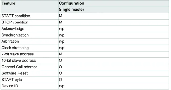
Table 2. Applicability of I2C-bus protocol features
M = mandatory; O = optional; n/a = not applicable.
Feature Configuration
Single master Multi-master Slave[1]
START condition M M M
STOP condition M M M
Acknowledge M M M
Synchronization n/a M n/a
Arbitration n/a M n/a
Clock stretching O[2] O[2] O
7-bit slave address M M M
10-bit slave address O O O
General Call address O O O
Software Reset O O O
START byte n/a O[3] n/a
Device ID n/a n/a O
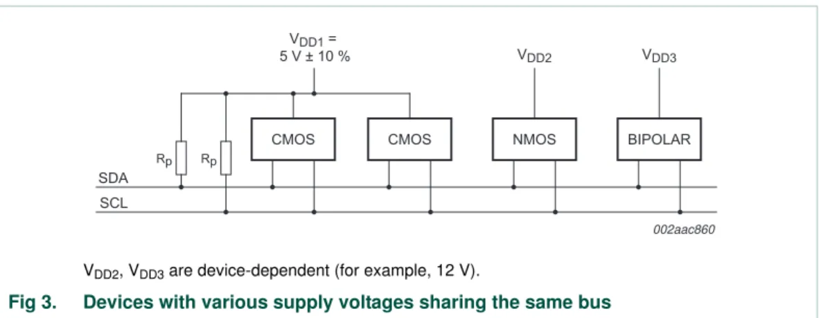
VDD2, VDD3 are device-dependent (for example, 12 V).
Fig 3. Devices with various supply voltages sharing the same bus
CMOS CMOS NMOS BIPOLAR
002aac860
VDD1 = 5 V ± 10 %
Rp Rp SDA
SCL
3.1.2 SDA and SCL logic levels
Due to the variety of different technology devices (CMOS, NMOS, bipolar) that can be connected to the I2C-bus, the levels of the logical ‘0’ (LOW) and ‘1’ (HIGH) are not fixed
and depend on the associated level of VDD. Input reference levels are set as 30 % and 70 % of VDD; VIL is 0.3VDD and VIH is 0.7VDD. See Figure 38, timing diagram. Some
legacy device input levels were fixed at VIL= 1.5 V and VIH= 3.0 V, but all new devices
require this 30 %/70 % specification. See Section 6 for electrical specifications.
3.1.3 Data validity
The data on the SDA line must be stable during the HIGH period of the clock. The HIGH or LOW state of the data line can only change when the clock signal on the SCL line is LOW (see Figure 4). One clock pulse is generated for each data bit transferred.
3.1.4 START and STOP conditions
All transactions begin with a START (S) and are terminated by a STOP (P) (see Figure 5). A HIGH to LOW transition on the SDA line while SCL is HIGH defines a START condition. A LOW to HIGH transition on the SDA line while SCL is HIGH defines a STOP condition.
START and STOP conditions are always generated by the master. The bus is considered to be busy after the START condition. The bus is considered to be free again a certain time after the STOP condition. This bus free situation is specified in Section 6.
The bus stays busy if a repeated START (Sr) is generated instead of a STOP condition. In this respect, the START (S) and repeated START (Sr) conditions are functionally identical. For the remainder of this document, therefore, the S symbol is used as a generic term to represent both the START and repeated START conditions, unless Sr is particularly relevant.
Fig 4. Bit transfer on the I2C-bus
mba607 data line
stable; data valid
change of data allowed SDA
SCL
Fig 5. START and STOP conditions
mba608 SDA
SCL
P
STOP condition S
Detection of START and STOP conditions by devices connected to the bus is easy if they incorporate the necessary interfacing hardware. However, microcontrollers with no such interface have to sample the SDA line at least twice per clock period to sense the transition.
3.1.5 Byte format
Every byte put on the SDA line must be eight bits long. The number of bytes that can be transmitted per transfer is unrestricted. Each byte must be followed by an Acknowledge bit. Data is transferred with the Most Significant Bit (MSB) first (see Figure 6). If a slave cannot receive or transmit another complete byte of data until it has performed some other function, for example servicing an internal interrupt, it can hold the clock line SCL LOW to force the master into a wait state. Data transfer then continues when the slave is ready for another byte of data and releases clock line SCL.
3.1.6 Acknowledge (ACK) and Not Acknowledge (NACK)
The acknowledge takes place after every byte. The acknowledge bit allows the receiver to signal the transmitter that the byte was successfully received and another byte may be sent. The master generates all clock pulses, including the acknowledge ninth clock pulse.
The Acknowledge signal is defined as follows: the transmitter releases the SDA line during the acknowledge clock pulse so the receiver can pull the SDA line LOW and it remains stable LOW during the HIGH period of this clock pulse (see Figure 4). Set-up and hold times (specified in Section 6) must also be taken into account.
When SDA remains HIGH during this ninth clock pulse, this is defined as the Not
Acknowledge signal. The master can then generate either a STOP condition to abort the transfer, or a repeated START condition to start a new transfer. There are five conditions that lead to the generation of a NACK:
1. No receiver is present on the bus with the transmitted address so there is no device to respond with an acknowledge.
2. The receiver is unable to receive or transmit because it is performing some real-time function and is not ready to start communication with the master.
3. During the transfer, the receiver gets data or commands that it does not understand.
4. During the transfer, the receiver cannot receive any more data bytes.
5. A master-receiver must signal the end of the transfer to the slave transmitter.
Fig 6. Data transfer on the I2C-bus
S or Sr Sr or P
SDA
SCL
MSB
1 2 7 8 9 1 2 3 to 8 9
ACK ACK
002aac861 START or
repeated START condition
STOP or repeated START
condition acknowledgement
signal from slave
byte complete, interrupt within slave
clock line held LOW while interrupts are serviced
P
3.1.7 Clock synchronization
Two masters can begin transmitting on a free bus at the same time and there must be a method for deciding which takes control of the bus and complete its transmission. This is done by clock synchronization and arbitration. In single master systems, clock
synchronization and arbitration are not needed.
Clock synchronization is performed using the wired-AND connection of I2C interfaces to
the SCL line. This means that a HIGH to LOW transition on the SCL line causes the masters concerned to start counting off their LOW period and, once a master clock has gone LOW, it holds the SCL line in that state until the clock HIGH state is reached (see
Figure 7). However, if another clock is still within its LOW period, the LOW to HIGH
transition of this clock may not change the state of the SCL line. The SCL line is therefore held LOW by the master with the longest LOW period. Masters with shorter LOW periods enter a HIGH wait-state during this time.
When all masters concerned have counted off their LOW period, the clock line is released and goes HIGH. There is then no difference between the master clocks and the state of the SCL line, and all the masters start counting their HIGH periods. The first master to complete its HIGH period pulls the SCL line LOW again.
In this way, a synchronized SCL clock is generated with its LOW period determined by the master with the longest clock LOW period, and its HIGH period determined by the one with the shortest clock HIGH period.
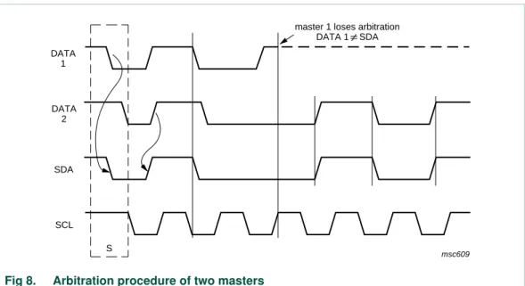
3.1.8 Arbitration
Arbitration, like synchronization, refers to a portion of the protocol required only if more than one master is used in the system. Slaves are not involved in the arbitration procedure. A master may start a transfer only if the bus is free. Two masters may generate a START condition within the minimum hold time (tHD;STA) of the START
condition which results in a valid START condition on the bus. Arbitration is then required to determine which master will complete its transmission.
Arbitration proceeds bit by bit. During every bit, while SCL is HIGH, each master checks to see if the SDA level matches what it has sent. This process may take many bits. Two
Fig 7. Clock synchronization during the arbitration procedure CLK
1
CLK 2
SCL
counter reset
wait state
start counting HIGH period
transmissions are identical. The first time a master tries to send a HIGH, but detects that the SDA level is LOW, the master knows that it has lost the arbitration and turns off its SDA output driver. The other master goes on to complete its transaction.
No information is lost during the arbitration process. A master that loses the arbitration can generate clock pulses until the end of the byte in which it loses the arbitration and must restart its transaction when the bus is free.
If a master also incorporates a slave function and it loses arbitration during the addressing stage, it is possible that the winning master is trying to address it. The losing master must therefore switch over immediately to its slave mode.
Figure 8 shows the arbitration procedure for two masters. More may be involved
depending on how many masters are connected to the bus. The moment there is a difference between the internal data level of the master generating DATA1 and the actual level on the SDA line, the DATA1 output is switched off. This does not affect the data transfer initiated by the winning master.
Since control of the I2C-bus is decided solely on the address and data sent by competing
masters, there is no central master, nor any order of priority on the bus.
There is an undefined condition if the arbitration procedure is still in progress at the moment when one master sends a repeated START or a STOP condition while the other master is still sending data. In other words, the following combinations result in an undefined condition:
•
Master 1 sends a repeated START condition and master 2 sends a data bit.•
Master 1 sends a STOP condition and master 2 sends a data bit.•
Master 1 sends a repeated START condition and master 2 sends a STOP condition.Fig 8. Arbitration procedure of two masters
msc609 DATA
1
DATA 2
SDA
SCL
S
3.1.9 Clock stretching
Clock stretching pauses a transaction by holding the SCL line LOW. The transaction cannot continue until the line is released HIGH again. Clock stretching is optional and in fact, most slave devices do not include an SCL driver so they are unable to stretch the clock.
On the byte level, a device may be able to receive bytes of data at a fast rate, but needs more time to store a received byte or prepare another byte to be transmitted. Slaves can then hold the SCL line LOW after reception and acknowledgment of a byte to force the master into a wait state until the slave is ready for the next byte transfer in a type of handshake procedure (see Figure 7).
On the bit level, a device such as a microcontroller with or without limited hardware for the I2C-bus, can slow down the bus clock by extending each clock LOW period. The speed of
any master is adapted to the internal operating rate of this device.
In Hs-mode, this handshake feature can only be used on byte level (see Section 5.3.2).
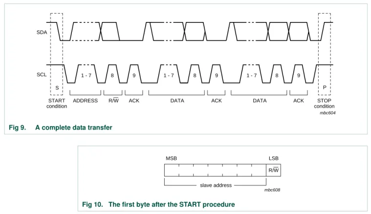
3.1.10 The slave address and R/W bit
Data transfers follow the format shown in Figure 9. After the START condition (S), a slave address is sent. This address is seven bits long followed by an eighth bit which is a data direction bit (R/W) — a ‘zero’ indicates a transmission (WRITE), a ‘one’ indicates a request for data (READ) (refer to Figure 10). A data transfer is always terminated by a STOP condition (P) generated by the master. However, if a master still wishes to communicate on the bus, it can generate a repeated START condition (Sr) and address another slave without first generating a STOP condition. Various combinations of read/write formats are then possible within such a transfer.
Fig 9. A complete data transfer S
1 - 7 8 9 1 - 7 8 9 1 - 7 8 9
P
STOP condition START
condition
DATA ACK
DATA ACK
ADDRESS R/W ACK SDA
SCL
mbc604
mbc608 R/W LSB MSB
Possible data transfer formats are:
•
Master-transmitter transmits to slave-receiver. The transfer direction is not changed (see Figure 11). The slave receiver acknowledges each byte.•
Master reads slave immediately after first byte (see Figure 12). At the moment of the first acknowledge, the master-transmitter becomes a master-receiver and the slave-receiver becomes a slave-transmitter. This first acknowledge is still generated by the slave. The master generates subsequent acknowledges. The STOP condition is generated by the master, which sends a not-acknowledge (A) just before the STOP condition.•
Combined format (see Figure 13). During a change of direction within a transfer, the START condition and the slave address are both repeated, but with the R/W bit reversed. If a master-receiver sends a repeated START condition, it sends a not-acknowledge (A) just before the repeated START condition.Notes:
1. Combined formats can be used, for example, to control a serial memory. The internal memory location must be written during the first data byte. After the START condition and slave address is repeated, data can be transferred.
2. All decisions on auto-increment or decrement of previously accessed memory locations, etc., are taken by the designer of the device.
3. Each byte is followed by an acknowledgment bit as indicated by the A or A blocks in the sequence.
4. I2C-bus compatible devices must reset their bus logic on receipt of a START or
repeated START condition such that they all anticipate the sending of a slave address, even if these START conditions are not positioned according to the proper format.
5. A START condition immediately followed by a STOP condition (void message) is an illegal format. Many devices however are designed to operate properly under this condition.
6. Each device connected to the bus is addressable by a unique address. Normally a simple master/slave relationship exists, but it is possible to have multiple identical slaves that can receive and respond simultaneously, for example in a group broadcast. This technique works best when using bus switching devices like the PCA9546A where all four channels are on and identical devices are configured at the same time, understanding that it is impossible to determine that each slave
3.1.11 10-bit addressing
10-bit addressing expands the number of possible addresses. Devices with 7-bit and 10-bit addresses can be connected to the same I2C-bus, and both 7-bit and 10-bit
addressing can be used in all bus speed modes. Currently, 10-bit addressing is not being widely used.
The 10-bit slave address is formed from the first two bytes following a START condition (S) or a repeated START condition (Sr).
The first seven bits of the first byte are the combination 1111 0XX of which the last two bits (XX) are the two Most-Significant Bits (MSB) of the 10-bit address; the eighth bit of the first byte is the R/W bit that determines the direction of the message.
Although there are eight possible combinations of the reserved address bits 1111 XXX,
Fig 11. A master-transmitter addressing a slave receiver with a 7-bit address (the transfer direction is not changed)
Fig 12. A master reads a slave immediately after the first byte
Fig 13. Combined format
mbc605
A/A A
'0' (write)
data transferred (n bytes + acknowledge)
A = acknowledge (SDA LOW) A = not acknowledge (SDA HIGH) S = START condition
P = STOP condition R/W
from master to slave
from slave to master
DATA DATA A SLAVE ADDRESS S P mbc606 A (read) data transferred (n bytes + acknowledge)
R/W A 1 P DATA DATA SLAVE ADDRESS S A mbc607 DATA A R/W
read or write
A/A DATA A R/W (n bytes + ack.)*
direction of transfer may change at this point.
read or write (n bytes
+ ack.)*
Sr = repeated START condition A/A
*not shaded because transfer direction of data and acknowledge bits depends on R/W bits.
SLAVE ADDRESS
All combinations of read/write formats previously described for 7-bit addressing are possible with 10-bit addressing. Two are detailed here:
•
Master-transmitter transmits to slave-receiver with a 10-bit slave address.The transfer direction is not changed (see Figure 14). When a 10-bit address follows a START condition, each slave compares the first seven bits of the first byte of the slave address (1111 0XX) with its own address and tests if the eighth bit (R/W direction bit) is 0. It is possible that more than one device finds a match and generate an acknowledge (A1). All slaves that found a match compare the eight bits of the second byte of the slave address (XXXX XXXX) with their own addresses, but only one slave finds a match and generates an acknowledge (A2). The matching slave remains addressed by the master until it receives a STOP condition (P) or a repeated START condition (Sr) followed by a different slave address.
•
Master-receiver reads slave-transmitter with a 10-bit slave address.The transfer direction is changed after the second R/W bit (Figure 15). Up to and including acknowledge bit A2, the procedure is the same as that described for a master-transmitter addressing a slave-receiver. After the repeated START condition (Sr), a matching slave remembers that it was addressed before. This slave then checks if the first seven bits of the first byte of the slave address following Sr are the same as they were after the START condition (S), and tests if the eighth (R/W) bit is 1. If there is a match, the slave considers that it has been addressed as a transmitter and generates acknowledge A3. The slave-transmitter remains addressed until it receives a STOP condition (P) or until it receives another repeated START condition (Sr) followed by a different slave address. After a repeated START condition (Sr), all the other slave devices will also compare the first seven bits of the first byte of the slave address (1111 0XX) with their own addresses and test the eighth (R/W) bit. However, none of them will be addressed because R/W = 1 (for 10-bit devices), or the 1111 0XX slave address (for 7-bit devices) does not match.
Slave devices with 10-bit addressing react to a ‘general call’ in the same way as slave devices with 7-bit addressing. Hardware masters can transmit their 10-bit address after a ‘general call’. In this case, the ‘general call’ address byte is followed by two successive bytes containing the 10-bit address of the master-transmitter. The format is as shown in
Figure 15 where the first DATA byte contains the eight least-significant bits of the master
address.
Fig 14. A master-transmitter addresses a slave-receiver with a 10-bit address
mbc613 R/W A1
(write)
A2 A A/A
1 1 1 1 0 X X 0
SLAVE ADDRESS 1st 7 BITS
S SLAVE ADDRESS DATA DATA P
2nd BYTE
Fig 15. A master-receiver addresses a slave-transmitter with a 10-bit address
mbc614 R/W A1
(write)
A3 DATA DATA
A2 R/W
(read) 1 1 1 1 0 X X 0 1 1 1 1 0 X X 1
A
A P
Sr SLAVE ADDRESS
1st 7 BITS
SLAVE ADDRESS 2nd BYTE
The START byte 0000 0001 (01h) can precede the 10-bit addressing in the same way as for 7-bit addressing (see Section 3.1.15).
3.1.12 Reserved addresses
Two groups of eight addresses (0000 XXX and 1111 XXX) are reserved for the purposes shown in Table 3.
[1] The general call address is used for several functions including software reset. [2] No device is allowed to acknowledge at the reception of the START byte.
[3] The CBUS address has been reserved to enable the inter-mixing of CBUS compatible and I2C-bus
compatible devices in the same system. I2C-bus compatible devices are not allowed to respond on
reception of this address.
[4] The address reserved for a different bus format is included to enable I2C and other protocols to be mixed.
Only I2C-bus compatible devices that can work with such formats and protocols are allowed to respond to
this address.
Assignment of addresses within a local system is up to the system architect who must take into account the devices being used on the bus and any future interaction with other conventional I2C-buses. For example, a device with seven user-assignable address pins
allows all 128 addresses to be assigned. If it is known that the reserved address is never going to be used for its intended purpose, a reserved address can be used for a slave address.
3.1.13 General call address
The general call address is for addressing every device connected to the I2C-bus at the
same time. However, if a device does not need any of the data supplied within the general call structure, it can ignore this address by not issuing an acknowledgment. If a device does require data from a general call address, it acknowledges this address and behave as a slave-receiver. The master does not actually know how many devices acknowledged if one or more devices respond. The second and following bytes are acknowledged by every slave-receiver capable of handling this data. A slave who cannot process one of these bytes must ignore it by not-acknowledging. Again, if one or more slaves
acknowledge, the not-acknowledge will not be seen by the master. The meaning of the general call address is always specified in the second byte (see Figure 16).
Table 3. Reserved addresses
X = don’t care; 1 = HIGH; 0 = LOW.
Slave address R/W bit Description
0000 000 0 general call address[1]
0000 000 1 START byte[2]
0000 001 X CBUS address[3]
0000 010 X reserved for different bus format[4]
0000 011 X reserved for future purposes
0000 1XX X Hs-mode master code
1111 1XX 1 device ID
There are two cases to consider:
•
When the least significant bit B is a ‘zero’.•
When the least significant bit B is a ‘one’.When bit B is a ‘zero’, the second byte has the following definition:
•
0000 0110 (06h): Reset and write programmable part of slave address byhardware. On receiving this 2-byte sequence, all devices designed to respond to the
general call address reset and take in the programmable part of their address. Precautions must be taken to ensure that a device is not pulling down the SDA or SCL line after applying the supply voltage, since these low levels would block the bus.
•
0000 0100 (04h): Write programmable part of slave address by hardware.Behaves as above, but the device does not reset.
•
0000 0000 (00h): This code is not allowed to be used as the second byte.Sequences of programming procedure are published in the appropriate device data sheets. The remaining codes have not been fixed and devices must ignore them.
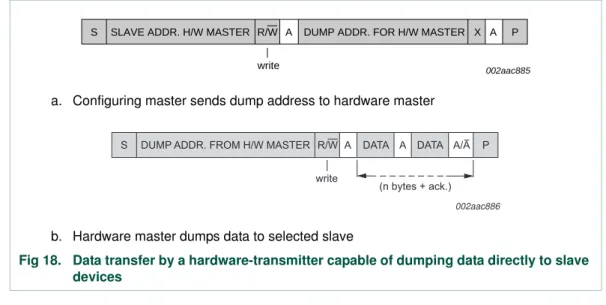
When bit B is a ‘one’, the 2-byte sequence is a ‘hardware general call’. This means that the sequence is transmitted by a hardware master device, such as a keyboard scanner, which can be programmed to transmit a desired slave address. Since a hardware master does not know in advance to which device the message has to be transferred, it can only generate this hardware general call and its own address — identifying itself to the system (see Figure 17).
The seven bits remaining in the second byte contain the address of the hardware master. This address is recognized by an intelligent device (for example, a microcontroller) connected to the bus which then accepts the information from the hardware master. If the hardware master can also act as a slave, the slave address is identical to the master address.
Fig 16. General call address format
Fig 17. Data transfer from a hardware master-transmitter
mbc623 LSB
second byte
0 0 0 0 0 0 0 0 A X X X X X X X B A
first byte (general call address)
mbc624 general
call address
(B)
A A
second byte
A A
In some systems, an alternative could be that the hardware master transmitter is set in the slave-receiver mode after the system reset. In this way, a system configuring master can tell the hardware master-transmitter (which is now in slave-receiver mode) to which address data must be sent (see Figure 18). After this programming procedure, the hardware master remains in the master-transmitter mode.
3.1.14 Software reset
Following a General Call, (0000 0000), sending 0000 0110 (06h) as the second byte causes a software reset. This feature is optional and not all devices respond to this command. On receiving this 2-byte sequence, all devices designed to respond to the general call address reset and take in the programmable part of their address.
Precautions must be taken to ensure that a device is not pulling down the SDA or SCL line after applying the supply voltage, since these low levels would block the bus.
3.1.15 START byte
Microcontrollers can be connected to the I2C-bus in two ways. A microcontroller with an
on-chip hardware I2C-bus interface can be programmed to be only interrupted by requests
from the bus. When the device does not have such an interface, it must constantly monitor the bus via software. Obviously, the more times the microcontroller monitors, or polls the bus, the less time it can spend carrying out its intended function.
There is therefore a speed difference between fast hardware devices and a relatively slow microcontroller which relies on software polling.
In this case, data transfer can be preceded by a start procedure which is much longer than normal (see Figure 19). The start procedure consists of:
•
A START condition (S)•
A START byte (0000 0001)•
An acknowledge clock pulse (ACK)•
A repeated START condition (Sr).a. Configuring master sends dump address to hardware master
b. Hardware master dumps data to selected slave
Fig 18. Data transfer by a hardware-transmitter capable of dumping data directly to slave devices
002aac885 write
A A
R/W
S SLAVE ADDR. H/W MASTER DUMP ADDR. FOR H/W MASTER X P
002aac886
R/W
write
A A
(n bytes + ack.) A/A
After the START condition S has been transmitted by a master which requires bus access, the START byte (0000 0001) is transmitted. Another microcontroller can therefore sample the SDA line at a low sampling rate until one of the seven zeros in the START byte is detected. After detection of this LOW level on the SDA line, the microcontroller can switch to a higher sampling rate to find the repeated START condition Sr which is then used for synchronization.
A hardware receiver resets upon receipt of the repeated START condition Sr and therefore ignores the START byte.
An acknowledge-related clock pulse is generated after the START byte. This is present only to conform with the byte handling format used on the bus. No device is allowed to acknowledge the START byte.
3.1.16 Bus clear
In the unlikely event where the clock (SCL) is stuck LOW, the preferential procedure is to reset the bus using the HW reset signal if your I2C devices have HW reset inputs. If the
I2C devices do not have HW reset inputs, cycle power to the devices to activate the
mandatory internal Power-On Reset (POR) circuit.
If the data line (SDA) is stuck LOW, the master should send nine clock pulses. The device that held the bus LOW should release it sometime within those nine clocks. If not, then use the HW reset or cycle power to clear the bus.
3.1.17 Device ID
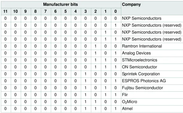
The Device ID field (see Figure 20) is an optional 3-byte read-only (24 bits) word giving the following information:
•
Twelve bits with the manufacturer name, unique per manufacturer (for example, NXP)•
Nine bits with the part identification, assigned by manufacturer (for example,PCA9698)
•
Three bits with the die revision, assigned by manufacturer (for example, RevX)Fig 19. START byte procedure
002aac997
S
9 8 2
1
Sr 7
NACK dummy acknowledge
(HIGH)
START byte 0000 0001 SDA
The Device ID is read-only, hard-wired in the device and can be accessed as follows:
1. START condition
2. The master sends the Reserved Device ID I2C-bus address followed by the R/W bit
set to ‘0’ (write): ‘1111 1000’.
3. The master sends the I2C-bus slave address of the slave device it must identify. The
LSB is a ‘Don’t care’ value. Only one device must acknowledge this byte (the one that has the I2C-bus slave address).
4. The master sends a Re-START condition.
Remark: A STOP condition followed by a START condition resets the slave state
machine and the Device ID Read cannot be performed. Also, a STOP condition or a Re-START condition followed by an access to another slave device resets the slave state machine and the Device ID Read cannot be performed.
5. The master sends the Reserved Device ID I2C-bus address followed by the R/W bit
set to ‘1’ (read): ‘1111 1001’.
6. The Device ID Read can be done, starting with the 12 manufacturer bits (first byte + four MSBs of the second byte), followed by the nine part identification bits (four LSBs of the second byte + five MSBs of the third byte), and then the three die revision bits (three LSBs of the third byte).
7. The master ends the reading sequence by NACKing the last byte, thus resetting the slave device state machine and allowing the master to send the STOP condition.
Remark: The reading of the Device ID can be stopped anytime by sending a NACK.
If the master continues to ACK the bytes after the third byte, the slave rolls back to the first byte and keeps sending the Device ID sequence until a NACK has been detected.
Fig 20. Device ID field
0
002aab942 0 0
0
0 0 0 0 0 0 0
0
0 0 0 0 0 0 0
revision
0
0 0 0 0
Designers of new I2C devices who want to implement the device ID feature should contact
NXP at [email protected] to have a unique manufacturer ID assigned.
Table 4. Assigned manufacturer IDs
Manufacturer bits Company
11 10 9 8 7 6 5 4 3 2 1 0
0 0 0 0 0 0 0 0 0 0 0 0 NXP Semiconductors
0 0 0 0 0 0 0 0 0 0 0 1 NXP Semiconductors (reserved)
0 0 0 0 0 0 0 0 0 0 1 0 NXP Semiconductors (reserved)
0 0 0 0 0 0 0 0 0 0 1 1 NXP Semiconductors (reserved)
0 0 0 0 0 0 0 0 0 1 0 0 Ramtron International
0 0 0 0 0 0 0 0 0 1 0 1 Analog Devices
0 0 0 0 0 0 0 0 0 1 1 0 STMicroelectronics
0 0 0 0 0 0 0 0 0 1 1 1 ON Semiconductor
0 0 0 0 0 0 0 0 1 0 0 0 Sprintek Corporation
0 0 0 0 0 0 0 0 1 0 0 1 ESPROS Photonics AG
0 0 0 0 0 0 0 0 1 0 1 0 Fujitsu Semiconductor
0 0 0 0 0 0 0 0 1 0 1 1 Flir
0 0 0 0 0 0 0 0 1 1 0 0 O2Micro
3.2 Ultra Fast-mode I
2C-bus protocol
The UFm I2C-bus is a 2-wire push-pull serial bus that operates from DC to 5 MHz
transmitting data in one direction. It is most useful for speeds greater than 1 MHz to drive LED controllers and other devices that do not need feedback. The UFm I2C-bus protocol
is based on the standard I2C-bus protocol that consists of a START, slave address,
command bit, ninth clock, and a STOP bit. The command bit is a ‘write’ only, and the data bit on the ninth clock is driven HIGH, ignoring the ACK cycle due to the unidirectional nature of the bus. The 2-wire push-pull driver consists of a UFm serial clock (USCL) and serial data (USDA).
Slave devices contain a unique address (whether it is a microcontroller, LCD driver, LED controller, GPO) and operate only as receivers. An LED driver may be only a receiver and can be supported by UFm, whereas a memory can both receive and transmit data and is not supported by UFm.
Since UFm I2C-bus uses push-pull drivers, it does not have the multi-master capability of
the wired-AND open-drain Sm, Fm, and Fm+ I2C-buses. In UFm, a master is the only
device that initiates a data transfer on the bus and generates the clock signals to permit that transfer. All other devices addressed are considered slaves.
Let us consider the case of a data transfer between a master and multiple slaves connected to the UFm I2C-bus (see Figure 21).
Table 5. Definition of UFm I2C-bus terminology
Term Description
Transmitter the device that sends data to the bus
Receiver the device that receives data from the bus
Master the device that initiates a transfer, generates clock signals and terminates a transfer
Slave the device addressed by a master
Fig 21. Example of UFm I2C-bus configuration
002aag654
USDA
USCL
Master ASIC LED
controller 3 LCD
DRIVER
LED controller 1
LED
This highlights the master/transmitter-slave/receiver relationship found on the UFm I2C-bus. Note that these relationships are permanent, as data transfer is only permitted in
one direction. The transfer of data would proceed as follows:
Suppose that the master ASIC wants to send information to the LED controller 2:
•
ASIC A (master-transmitter), addresses LED controller 2 (slave-receiver) by sending the address on the USDA and generating the clock on USCL.•
ASIC A (master-transmitter), sends data to LED controller 2 (slave-receiver) on the USDA and generates the clock on USCL.•
ASIC A terminates the transfer.The possibility of connecting more than one UFm master to the UFm I2C-bus is not
allowed due to bus contention on the push-pull outputs. If an additional master is required in the system, it must be fully isolated from the other master (that is, with a true ‘one hot’ MUX) as only one master is allowed on the bus at a time.
Generation of clock signals on the UFm I2C-bus is always the responsibility of the master
device, that is, the master generates the clock signals when transferring data on the bus. Bus clock signals from a master cannot be altered by a slave device with clock stretching and the process of arbitration and clock synchronization does not exist within the UFm I2C-bus.
Table 6 summarizes the use of mandatory and optional portions of the UFm I2C-bus
specification.
Table 6. Applicability of I2C-bus features to UFm
M = mandatory; O = optional; n/p = not possible
Feature Configuration
Single master
START condition M
STOP condition M
Acknowledge n/p
Synchronization n/p
Arbitration n/p
Clock stretching n/p
7-bit slave address M
10-bit slave address O
General Call address O
Software Reset O
START byte O
3.2.1 USDA and USCL signals
Both USDA and USCL are unidirectional lines, with push-pull outputs. When the bus is free, both lines are pulled HIGH by the upper transistor of the output stage. Data on the I2C-bus can be transferred at rates of up to 5000 kbit/s in the Ultra Fast-mode. The
number of interfaces connected to the bus is limited by the bus loading, reflections from cable ends, connectors, and stubs.
3.2.2 USDA and USCL logic levels
Due to the variety of different technology devices (CMOS, NMOS, bipolar) that can be connected to the I2C-bus, the levels of the logical ‘0’ (LOW) and ‘1’ (HIGH) are not fixed
and depend on the associated level of VDD. Input reference levels are set as 30 % and
70 % of VDD; VIL is 0.3VDD and VIH is 0.7VDD. See Figure 40, timing diagram. See
Section 6 for electrical specifications.
3.2.3 Data validity
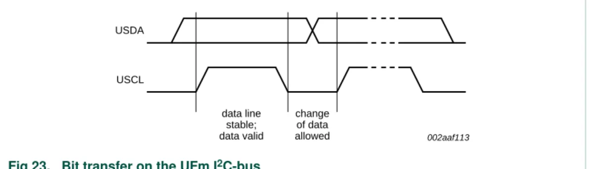
The data on the USDA line must be stable during the HIGH period of the clock. The HIGH or LOW state of the data line can only change when the clock signal on the USCL line is LOW (see Figure 23). One clock pulse is generated for each data bit transferred.
3.2.4 START and STOP conditions
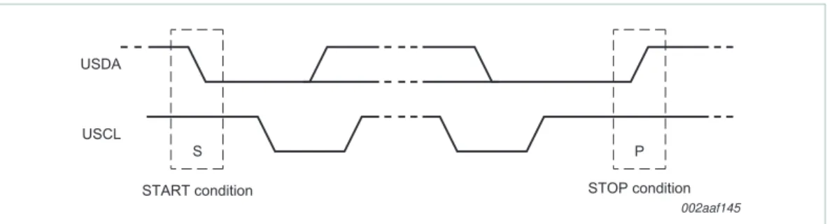
Both data and clock lines remain HIGH when the bus is not busy. All transactions begin with a START (S) and can be terminated by a STOP (P) (see Figure 24). A HIGH to LOW transition on the USDA line while USCL is HIGH defines a START condition. A LOW to HIGH transition on the USDA line while USCL is HIGH defines a STOP condition.
Fig 22. Simplified schematic of USCL, USDA outputs
002aag655
VDD(IO)
VSS
USCL or USDA pin
Fig 23. Bit transfer on the UFm I2C-bus
002aaf113 data line
stable; data valid
change of data allowed USDA
START and STOP conditions are always generated by the master. The bus is considered to be busy after the START condition. The bus is considered to be free again a certain time after the STOP condition. This bus free situation is specified in Section 6. The bus stays busy if a repeated START (Sr) is generated instead of a STOP condition. In this respect, the START (S) and repeated START (Sr) conditions are functionally identical. For the remainder of this document, therefore, the S symbol is used as a generic term to represent both the START and repeated START conditions, unless Sr is particularly relevant.
Detection of START and STOP conditions by devices connected to the bus is easy if they incorporate the necessary interfacing hardware. However, microcontrollers with no such interface have to sample the USDA line at least twice per clock period to sense the transition.
3.2.5 Byte format
Every byte put on the USDA line must be eight bits long. The number of bytes that can be transmitted per transfer is unrestricted. The master drives the USDA HIGH after each byte during the Acknowledge cycle. Data is transferred with the Most Significant Bit (MSB) first (see Figure 25). A slave is not allowed to hold the clock LOW if it cannot receive another complete byte of data or while it is performing some other function, for example servicing an internal interrupt.
Fig 24. Definition of START and STOP conditions for UFm I2C-bus
002aaf145
USDA
USCL
P
STOP condition S
START condition
Fig 25. Data transfer on the UFm I2C-bus
S or Sr Sr or P
USDA
USCL
MSB
1 2 8 9 1 2 3 to 7 8
NACK NACK
002aag657
START or repeated START
condition
STOP or repeated START
condition byte complete,
interrupt within slave
P
Sr Master drives the line HIGH on 9th clock cycle.
Slave never drives the USDA line.
3.2.6 Acknowledge (ACK) and Not Acknowledge (NACK)
Since the slaves are not able to respond the ninth clock cycle, the ACK and NACK are not required. However, the clock cycle is preserved in the UFm to be compatible with the I2C-bus protocol. The ACK and NACK are also referred to as the ninth clock cycle. The
master generates all clock pulses, including the ninth clock pulse. The ninth data bit is always driven HIGH (‘1’). Slave devices are not allowed to drive the SDA line at any time.
3.2.7 The slave address and R/W bit
Data transfers follow the format shown in Figure 26. After the START condition (S), a slave address is sent. This address is seven bits long followed by an eighth bit which is a data direction bit (W) — a ‘zero’ indicates a transmission (WRITE); a ‘one’ indicates a request for data (READ) and is not supported by UFm (except for the START byte,
Section 3.2.12) since the communication is unidirectional (refer to Figure 27). A data
transfer is always terminated by a STOP condition (P) generated by the master. However, if a master still wishes to communicate on the bus, it can generate a repeated START condition (Sr) and address another slave without first generating a STOP condition.
The UFm data transfer format is:
•
Master-transmitter transmits to slave-receiver. The transfer direction is not changed (see Figure 28). The master never acknowledges because it never receives any data but generates the ‘1’ on the ninth bit for the slave to conform to the I2C-bus protocol.Fig 26. A complete UFm data transfer
S
1 - 7 8 9 1 - 7 8 9 1 - 7 8 9
P
STOP condition START
condition
DATA NACK
DATA NACK
ADDRESS W NACK
USDA
USCL
002aag658
Fig 27. The first byte after the START procedure
002aag659
W LSB MSB
Notes:
1. Individual transaction or repeated START formats addressing multiple slaves in one transaction can be used. After the START condition and slave address is repeated, data can be transferred.
2. All decisions on auto-increment or decrement of previously accessed memory locations, etc., are taken by the designer of the device.
3. Each byte is followed by a Not-Acknowledgment bit as indicated by the A blocks in the sequence.
4. I2C-bus compatible devices must reset their bus logic on receipt of a START or
repeated START condition such that they all anticipate the sending of a slave address, even if these START conditions are not positioned according to the proper format.
5. A START condition immediately followed by a STOP condition (void message) is an illegal format. Many devices however are designed to operate properly under this condition.
6. Each device connected to the bus is addressable by a unique address. A simple master/slave relationship exists, but it is possible to have multiple identical slaves that can receive and respond simultaneously, for example, in a group broadcast where all identical devices are configured at the same time, understanding that it is impossible to determine that each slave is responsive. Refer to individual component data sheets.
3.2.8 10-bit addressing
10-bit addressing expands the number of possible addresses. Devices with 7-bit and 10-bit addresses can be connected to the same I2C-bus, and both 7-bit and 10-bit
addressing can be used in all bus speed modes.
The 10-bit slave address is formed from the first two bytes following a START condition (S) or a repeated START condition (Sr). The first seven bits of the first byte are the combination 1111 0XX of which the last two bits (XX) are the two Most Significant Bits (MSBs) of the 10-bit address; the eighth bit of the first byte is the R/W bit that determines the direction of the message.
Although there are eight possible combinations of the reserved address bits 1111 XXX, only the four combinations 1111 0XX are used for 10-bit addressing. The remaining four combinations 1111 1XX are reserved for future I2C-bus enhancements.
Fig 28. A master-transmitter addressing a slave receiver with a 7-bit address
002aag660
A
‘0’ (write)
data transferred (n bytes + not acknowledge)
A = not acknowledge (USDA HIGH) S = START condition
P = STOP condition W
from master to slave
DATA DATA
A SLAVE ADDRESS
Only the write format previously described for 7-bit addressing is possible with 10-bit addressing. Detailed here:
•
Master-transmitter transmits to slave-receiver with a 10-bit slave address. The transfer direction is not changed (see Figure 29). When a 10-bit address follows a START condition, each slave compares the first seven bits of the first byte of the slave address (1111 0XX) with its own address and tests if the eighth bit (R/W direction bit) is 0 (W). All slaves that found a match compare the eight bits of the second byte of the slave address (XXXX XXXX) with their own addresses, but only one slave finds a match. The matching slave remains addressed by the master until it receives a STOP condition (P) or a repeated START condition (Sr) followed by a different slave address.The START byte 0000 0001 (01h) can precede the 10-bit addressing in the same way as for 7-bit addressing (see Section 3.2.12).
3.2.9 Reserved addresses in UFm
The UFm I2C-bus has a different physical layer than the other I2C-bus modes. Therefore
the available slave address range is different. Two groups of eight addresses (0000 XXX and 1111 XXX) are reserved for the purposes shown in Table 7.
[1] The general call address is used for several functions including software reset. [2] No UFm device is allowed to acknowledge at the reception of the START byte.
Assignment of addresses within a local system is up to the system architect who must take into account the devices being used on the bus and any future interaction with reserved addresses. For example, a device with seven user-assignable address pins allows all 128 addresses to be assigned. If it is known that the reserved address is never going to be used for its intended purpose, then a reserved address can be used for a
Fig 29. A master-transmitter addresses a slave-receiver with a 10-bit address
002aag661
W A
(write)
A A NA
1 1 1 1 0 X X 0
SLAVE ADDRESS 1st 7 BITS
S SLAVE ADDRESS DATA DATA P
2nd BYTE
Table 7. Reserved addresses
X = don’t care; 1 = HIGH; 0 = LOW.
Slave address R/W bit Description
0000 000 0 general call address[1]
0000 000 1 START byte[2]
0000 001 X reserved for future purposes
0000 010 X reserved for future purposes
0000 011 X reserved for future purposes
0000 1XX X reserved for future purposes
1111 1XX X reserved for future purposes
3.2.10 General call address
The general call address is for addressing every device connected to the I2C-bus at the
same time. However, if a device does not need any of the data supplied within the general call structure, it can ignore this address. If a device does require data from a general call address, it behaves as a slave-receiver. The master does not actually know how many devices are responsive to the general call. The second and following bytes are received by every slave-receiver capable of handling this data. A slave that cannot process one of these bytes must ignore it. The meaning of the general call address is always specified in the second byte (see Figure 30).
There are two cases to consider:
•
When the least significant bit B is a ‘zero’•
When the least significant bit B is a ‘one’When bit B is a ‘zero’, the second byte has the following definition:
0000 0110 (06h) — Reset and write programmable part of slave address by hardware.
On receiving this 2-byte sequence, all devices designed to respond to the general call address reset and take in the programmable part of their address.
0000 0100 (04h) — Write programmable part of slave address by hardware. Behaves as
above, but the device does not reset.
0000 0000 (00h) — This code is not allowed to be used as the second byte.
Sequences of programming procedure are published in the appropriate device data sheets. The remaining codes have not been fixed and devices must ignore them.
When bit B is a ‘one’, the 2-byte sequence is ignored.
3.2.11 Software reset
Following a General Call, (0000 0000), sending 0000 0110 (06h) as the second byte causes a software reset. This feature is optional and not all devices respond to this command. On receiving this 2-byte sequence, all devices designed to respond to the general call address reset and take in the programmable part of their address.
3.2.12 START byte
Microcontrollers can be connected to the I2C-bus in two ways. A microcontroller with an
on-chip hardware I2C-bus interface can be programmed to be only interrupted by requests
from the bus. When the device does not have such an interface, it must constantly monitor the bus via software. Obviously, the more times the microcontroller monitors, or polls the bus, the less time it can spend carrying out its intended function.
There is therefore a speed difference between fast hardware devices and a relatively slow microcontroller which relies on software polling.
Fig 30. General call address format
002aag662
LSB
second byte
0 0 0 0 0 0 0 0 A X X X X X X X B A
In this case, data transfer can be preceded by a start procedure which is much longer than normal (see Figure 31). The start procedure consists of:
•
A START condition (S)•
A START byte (0000 0001)•
A Not Acknowledge clock pulse (NACK)•
A repeated START condition (Sr)After the START condition S has been transmitted by a master which requires bus access, the START byte (0000 0001) is transmitted. Another microcontroller can therefore sample the USDA line at a low sampling rate until one of the seven zeros in the START byte is detected. After detection of this LOW level on the USDA line, the microcontroller can switch to a higher sampling rate to find the repeated START condition Sr, which is then used for synchronization. A hardware receiver resets upon receipt of the repeated START condition Sr and therefore ignores the START byte. An acknowledge-related clock pulse is generated after the START byte. This is present only to conform with the byte handling format used on the bus. No device is allowed to acknowledge the START byte.
3.2.13 Unresponsive slave reset
In the unlikely event where the slave becomes unresponsive (for example, determined through external feedback, not through UFm I2C-bus), the preferential procedure is to
reset the slave by using the software reset command or the hardware reset signal. If the slaves do not support these features, then cycle power to the devices to activate the mandatory internal Power-On Reset (POR) circuit.
3.2.14 Device ID
The Device ID field is not supported in UFm.
Fig 31. START byte procedure
002aag663
S
9 8 2
1
Sr 7
NACK dummy acknowledge
(HIGH)
START byte 0000 0001 USDA
4. Other uses of the I
2C-bus communications protocol
The I2C-bus is used as the communications protocol for several system architectures.
These architectures have added command sets and application-specific extensions in addition to the base I2C specification. In general, simple I2C-bus devices such as I/O
extenders could be used in any one of these architectures since the protocol and physical interfaces are the same.
4.1 CBUS
compatibility
CBUS receivers can be connected to the Standard-mode I2C-bus. However, a third bus
line called DLEN must then be connected and the acknowledge bit omitted. Normally, I2C
transmissions are sequences of 8-bit bytes; CBUS compatible devices have different formats.
In a mixed bus structure, I2C-bus devices must not respond to the CBUS message. For
this reason, a special CBUS address (0000 001X) to which no I2C-bus compatible device
responds has been reserved. After transmission of the CBUS address, the DLEN line can be made active and a CBUS-format transmission sent. After the STOP condition, all devices are again ready to accept data.
Master-transmitters can send CBUS formats after sending the CBUS address. The transmission is ended by a STOP condition, recognized by all devices.
Remark: If the CBUS configuration is known, and expansion with CBUS compatible
devices is not foreseen, the designer is allowed to adapt the hold time to the specific requirements of the device(s) used.
4.2 SMBus - System Management Bus
The SMBus uses I2C hardware and I2C hardware addressing, but adds second-level
software for building special systems. In particular, its specifications include an Address Resolution Protocol that can make dynamic address allocations.
Dynamic reconfiguration of the hardware and software allow bus devices to be ‘hot-plugged’ and used immediately, without restarting the system. The devices are recognized automatically and assigned unique addresses. This advantage results in a plug-and-play user interface. In both those protocols, there is a very useful distinction made between a System Host and all the other devices in the system that can have the names and functions of masters or slaves.
SMBus is used today as a system management bus in most PCs. Developed by Intel and others in 1995, it modified some I2C electrical and software characteristics for better
compatibility with the quickly decreasing power supply budget of portable equipment. SMBus also has a ‘High Power’ version 2.0 that includes a 4 mA sink current that cannot be driven by I2C chips unless the pull-up resistor is sized to I2C-bus levels.
4.2.1 I
2C/SMBus compliancy
SMBus and I2C protocols are basically the same: A SMBus master is able to control I2C
devices and vice versa at the protocol level. The SMBus clock is defined from 10 kHz to 100 kHz while I2C can be 0 Hz to 100 kHz, 0 Hz to 400 kHz, 0 Hz to 1 MHz and
0 Hz to 3.4 MHz, depending on the mode. This means that an I2C-bus running at less
Logic levels are slightly different also: TTL for SMBus: LOW = 0.8 V and HIGH = 2.1 V, versus the 30 %/70 % VDD CMOS level for I2C. This is not a problem if V
DD> 3.0 V. If the
I2C device is below 3.0 V, then there could be a problem if the logic HIGH/LOW levels are
not properly recognized.
4.2.2 Time-out feature
SMBus has a time-out feature which resets devices if a communication takes too long. This explains the minimum clock frequency of 10 kHz to prevent locking up the bus. I2C
can be a ‘DC’ bus, meaning that a slave device stretches the master clock when
performing some routine while the master is accessing it. This notifies the master that the slave is busy but does not want to lose the communication. The slave device will allow continuation after its task is complete. There is no limit in the I2C-bus protocol as to how
long this delay can be, whereas for a SMBus system, it would be limited to 35 ms.
SMBus protocol just assumes that if something takes too long, then it means that there is a problem on the bus and that all devices must reset in order to clear this mode. Slave devices are not then allowed to hold the clock LOW too long.
4.2.3 Differences between SMBus 1.0 and SMBus 2.0
The SMBus specification defines two classes of electrical characteristics: low power and high power. The first class, originally defined in the SMBus 1.0 and 1.1 specifications, was designed primarily with Smart Batteries in mind, but could be used with other low-power devices.
The 2.0 version introduces an alternative higher power set of electrical characteristics. This class is appropriate for use when higher drive capability is required, for example with SMBus devices on PCI add-in cards and for connecting such cards across the PCI connector between each other and to SMBus devices on the system board.
Devices may be powered by the bus VDD or by another power source, VBus (as with, for
example, Smart Batteries), and will inter-operate as long as they adhere to the SMBus electrical specifications for their class.
NXP devices have a higher power set of electrical characteristics than SMBus 1.0. The main difference is the current sink capability with VOL= 0.4 V.
•
SMBus low power = 350µA•
SMBus high power = 4 mA•
I2C-bus = 3 mASMBus ‘high power’ devices and I2C-bus devices will work together if the pull-up resistor
is sized for 3 mA.