Enabling False Path Identification from RTL
for Reducing Design and Test Futileness
Hiroshi Iwata, Satoshi Ohtake and Hideo Fujiwara
Graduate School of Information Science, Nara Institute of Science and Technology 8916-5 Takayama, Ikoma, Nara 630-0192, Japan
Email:{ hiroshi-i, ohtake, fujiwara }@is.naist.jp
Abstract—Information on false paths is useful for design and test. Since identification of false paths at gate level is hard, several methods using high-level design information have been proposed. These methods are effective only if the correspon- dence between paths at register transfer level (RTL) and at gate level can be established. Until now, the correspondence has been established only by some restricted logic synthesis. In this paper, we propose a method for mapping RTL false paths to their corresponding gate level paths without such a specific logic synthesis.
Keywords-false path, high level testing, path mapping, func- tional equivalence
I. INTRODUCTION
For design and test of circuits, false path information is very valuable since it can be used for reducing the time required for logic synthesis, test generation and test application, and circuit area while also minimizing over- testing. From the perspective of design, circuit area and time required for logic synthesis can be made small by using false path information. From the testing point of view, since no test pattern can be generated for path delay faults on false paths, prior false path identification can greatly reduce ATPG time. Furthermore, since some path delay faults on false paths can become testable due to application of design for testability (DFT) and result in over-testing, this can be alleviated by false path identification.
Several false path identification methods at gate level for combinational circuits[1], [2], [3] and for sequential circuits[4], [5] have been proposed. However, since it is dif- ficult to apply false path identification methods at gate level for large circuits containing a tremendous number of paths, some methods using register transfer level (RTL) design information, instead of gate level, have been proposed[6]. Yoshikawa et al.[6] defined RTL false paths and proposed a method to identify them. However, these methods would be useful only if the correspondence between paths at RTL and paths at gate level can be established. Until now, the correspondence has been established through module interface preserving-logic synthesis (MIP-LS)[6]. Currently, using MIP-LS is the only way to guarantee information on the correspondence. However, it is not practical to restrict synthesis only to MIP-LS.
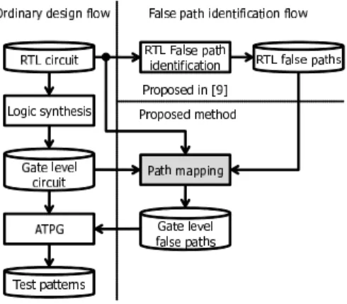
Figure 1. The false path identification flow.
In this paper, we focus on path mapping from a set of RTL false paths to gate level paths without considering MIP-LS. Figure 1 shows the false path identification flow. We first propose a method of mapping a set of RTL paths to its corresponding gate level paths (this is called path mapping) with an arbitrary logic synthesis independent of false paths. The proposed method maps RTL signal lines composing the RTL paths to gate level nets by using the functional equivalence relation of signal lines (this is called signal line mapping). The effort required for signal line mapping is alleviated by using the uniqueness of a set of the RTL paths and the rough candidate selection method. Because the number of signal lines that uniquely identify a set of RTL paths is much lower than that of whole signal lines in the set of RTL paths, and our path mapping algorithm only needs to map the reduced signal lines, the number of RTL signal lines to be mapped is significantly reduced. Signal line mapping is achieved by checking the equivalence between signal lines and all the gate level nets; however, it is obviously not practical. Therefore, we utilize the method that finds candidates of the functionally equivalent nets from a gate level circuit by using a diagnostics technique[7].
Since the gate level paths mapped by our method are represented as signal lines, each gate level path does not need to be fully specified as a path, so we are able to handle bundled paths. This representation is compatible with EDA tools, like Synopsys Design Constraint (SDC). Experimental results show that many RTL paths can be mapped to gate
テ キ ス ト The 5th IEEE Int. Symp. on Electronic Design, Test & Applications (DELTA 2010), pp. 20-25, Jan. 2010.
level paths using the proposed method within a reasonable time.
Then, we consider false path mapping. The definition of RTL false path in [6] assumes MIP-LS and the assumption guarantees that the corresponding gate level paths are false. In this paper, we show that any corresponding gate level path mapped from the set of RTL false paths by using the proposed method with an arbitrary logic synthesis is false. Experiments show that our path mapping method can establish the correspondences of RTL false paths and many gate level false paths.
The rest of this paper is organized as follows. Prelimi- naries are presented in Section II. Section III presents the proposed RTL path mapping method. Section IV shows that the gate level paths mapped from a set of RTL false paths with the proposed method are false. Experimental results are given in Section V. Section VI concludes the paper.
II. PRELIMINARIES
A. Circuit model
In this paper, we only consider structural RTL designs. A structural RTL design consists of a controller represented by a combinational module and a state register, and a datapath represented by RTL modules and signal lines connecting them, where an RTL module is an operational module, a register or a MUX and a signal line has an arbitrary bit width.
B. Gate level and RTL path representation
A gate level path is an ordered set of gate level nets {eG1, . . . , eGn} where eG1 is the net directly connected to a primary input or the output of an FF, eGn is the net directly connected to a primary output or the input of an FF, and eGi (i = 2, . . . , n − 1) is the net connecting the gates having eGi−1 as an input and eGi+1 as an output A subset of a gate level path pGis called a sub gate level path of pG.
Similarly, an RTL path is an ordered set of RTL signal lines!eR1, . . . , eRn" where eR1 is the RTL signal line directly connected to a primary input or the output of a register, eRn is the RTL signal line directly connected to a primary output or the input of a register, and eRi(i = 2, . . . , n − 1) is the RTL signal line connecting the modules having eRi−1 as an input and eRi+1as an output. A subset of an RTL path pRis called a sub RTL path of pR.
For an RTL signal line s, each one bit signal line separated from s is referred to as a bit-sliced RTL signal line of s. The i-th bit of s is represented as s[i]. A bit-sliced RTL path is an ordered set of bit-sliced RTL signal lines
!eR1[k1], . . . , eRn[kn]" where eR1[k1] is the k1-th bit-sliced RTL signal line directly connected to a primary input or the output of a register, eRn[kn] is the kn-th bit-sliced RTL signal line directly connected to a primary output or the input of a register, and eRi[ki](i = 2, . . . , n − 1) is the ki-th bit-sliced RTL signal line connecting the modules having eRi−1[ki−1]
Figure 2. Functionally equivalent signal lines s1and s2.
as an input and eRi+1[ki+1] as an output. A subset of a bit- sliced RTL path pR is called a sub bit-sliced RTL path of pR.
C. Relation between signal lines
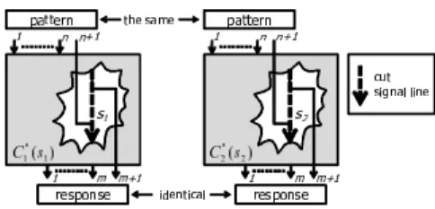
Here, we first define signal line cutting, which is an operation needed for defining functionally equivalent signal lines. For a combinational circuit C with n inputs, m outputs and an internal signal line s, the following operation is referred to as cutting C on s. Create the (n + 1)-th new input port and the(m + 1)-th new output port. Remove the signal line s. Create connections between(n + 1)-th input port and the end point of s and between the start point of s and the(m + 1)-th output port. In the following discussion, we represent the combinational circuit resulting from the above operations as C∗(s).
For two functionally equivalent combinational circuits, we define functional equivalence of signal lines as follows.
Definition 1 (Functionally equivalent signal line): For two functionally equivalent combinational circuits C1 and C2with internal signal lines s1and s2, respectively, s1and s2 are functionally equivalent if and only if C1∗(s1) and C2∗(s2) are functionally equivalent. ✷ In the following discussion, we represent the relation of functional equivalence between signal lines s1 and s2 as s1≡ls2.
Figure 2 illustrates functionally equivalent signal lines. The signal lines s1and s2are functionally equivalent if the responses from C1∗(s1) and C2∗(s2) are identical for any input pattern.
D. Relation between paths
We define the functional equivalence between a sub bit- sliced RTL path and a sub gate level path as follows.
Definition 2 (Functionally equivalent path): Sub bit- sliced RTL paths and sub gate level paths are simply referred to as sub paths. Sub paths q1= {e11, . . . , e1n} and q2 = {e21, . . . , e2m} are functionally equivalent if q1 and q2 satisfy the following conditions.
1) n= m
2) e1i≡le2i (i = 1, . . . , n) ✷ For mapping a given RTL path to gate level paths, it is sufficient to map only the RTL signal lines that uniquely identify the RTL path to gate level nets. Therefore, we provide the following definition to alleviate the signal line mapping effort.
Definition 3 (Identification of path): A sub RTL path qR is said to uniquely identify an RTL path pR if pR is the only
path that properly includes qR. ✷
Definition 4 (Identification of path set): A sub RTL path qR is said to uniquely identify a set of RTL paths, PR, if PR is the only set of RTL paths that properly includes qR.
✷
III. PROPOSED METHOD OF PATH MAPPING
In this section, we formulate the path mapping problem and present a solution to the problem independent of false paths. Consideration of false paths is described in Section IV.
A. Path mapping problem
We formulate the path mapping problem as a problem to find a set of gate level paths corresponding to a set of RTL paths. For solving path mapping problem, it is sufficient to consider only the RTL combinational circuit CR, which is the combinational part of a given structural RTL design SR, and the gate level combinational circuit CG, which is the combinational part of a gate level design synthesized from SR. We assume that there exists a one-to- one correspondence between the input/output signal lines of CRand CG. This relation is called I/O mapping information. The I/O mapping information of CRand CGcan be obtained by preserving all the bits of the registers in SRduring logic synthesis. The preservation is common for logic synthesis for structural RTL designs.
Definition 5 (Path mapping problem): Input • CR: an RTL combinational circuit
• CG: a gate level circuit that is functionally equivalent to CR
• The I/O mapping information between CRand CG
• PR: a set of RTL paths Output PG=
n
#
i=0 mi
#
j=0
PijG,
where PijG is defined as follows. Let qRi (i = 1, . . . , n) be a sub RTL path that uniquely identifies PRand qijR(j = 1, . . . , mi) be a sub bit-sliced RTL path of qiR where n is the number of the sub RTL paths of PR. Let qijGbe a sub gate level path that is functionally equivalent to qRij. PijG is a set of gate level paths including qGij. ✷ B. Path mapping algorithm
We propose an algorithm solving the path mapping prob- lem as follows. The algorithm establishes correspondences between a set of RTL paths, PR, and a set of gate level paths, PG.
1) Generate the minimum sub RTL path qiR(i = 1, . . . , n) that uniquely identifies PR.
2) Try to obtain a gate level net eGijk that is functionally equivalent to each bit-sliced RTL signal line eRijk(k = 1, . . . , l), where eRijk is an element of a bit-sliced RTL path qijR(j = 1, . . . , mi) of qRi , mi is the number of combinations of bit-sliced RTL paths obtained by specifying the bit portion of every RTL signal line on qRi, and l is the number of RTL signal lines on qRi. Go to step 3 if eGijk is obtained for all j and k of at least one sub RTL path qRi , i.e. all the RTL signal lines on some sub RTL path are mapped to gate level nets. (Otherwise, all qRi must be tried.)
3) Find all the gate level paths that include
!eGij1, . . . , eGijl", such that every eGijk(k = 1, . . . , l) is found in the previous step. The set of all the obtained gate level paths is referred to as PijG.
4) Calculate PG=
n
#
i=0 mi
#
j=0
PijG.
Note that, the signal line mapping in step 2 is described in the next subsection. We assume that at most one gate level net is functionally equivalent to a bit-sliced RTL signal line for simplifying the algorithm description. In our experiments reported in Section V, we did not face a case where more than one gate level net is mapped. However, we can handle multiple nets by taking into account all the paths that go through the nets. In step 3 and 4, not all the gate level paths need to be listed; it is not practical. Instead, paths are represented just by specifying nets,!eGij1, . . . , eGijl", that are passed through. This representation is compatible with EDA tools like SDC description.
C. Signal line mapping
In this section, we formulate the problem finding func- tionally equivalent nets. Then, we will show an algorithm for solving the problem. Signal line mapping algorithm is used in the proposed path mapping algorithm.
1) Signal line mapping problem: We formulate the signal line mapping problemto find a set of nets, which is func- tionally equivalent to a bit-sliced RTL signal line in an RTL circuit, in a gate level circuit.
Definition 6 (Signal line mapping problem): Input •CR: an RTL combinational circuit
•CG: a gate level circuit that is functionally equivalent to CR
•The I/O mapping information between CRand CG
•eR[k]: the k-th bit-sliced RTL signal line of an RTL signal line eR in CR
Output EG=!eG|eG≡leR[k]" where eGis a net in CG
✷ 2) Signal line mapping algorithm: Given an RTL com- binational circuit CR and a gate level combinational circuit CG, checking functional equivalence between a bit-sliced RTL signal line eR[k] in CR and a gate level net eGin CG can be performed by applying all the possible input patterns to both circuits CR∗(eR[k]) and CG∗(eG), and comparing
Figure 3. Relation between equivalent faults and functionality of respective signal lines.
their output responses. This is achieved by applying equiv- alence checking for CR∗(eR[k]) and CG∗(eG). However, it is not practical to explicitly check the functional equivalence for all the possible combinations between eR[k] and eG in CG.
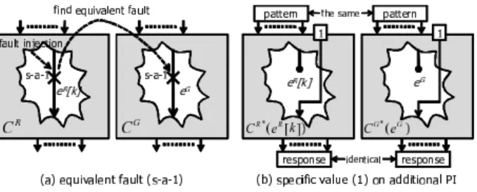
Ravi et al.[7] proposed a method of finding candidates for functionally equivalent nets of a given bit-sliced RTL signal line using fault diagnosis techniques. In this paper, their method is utilized to solve the signal line mapping problem. More specifically, their method injects a stuck-at fault on the bit-sliced RTL signal line and finds the stuck- at faults, which have identical behavior to the fault under the test patterns, in the gate level circuit. The faults in the gate level circuit and the fault in the RTL circuit are said to be equivalent. A necessary condition of functional equivalence is that the responses of the RTL circuit and the gate level circuit are identical when value v’s are fixed to eR[k] and eG, respectively (see Fig.3 (b)). It is the same situation when s-a-v faults are assumed to be presented on eR[k] and on eG, respectively (see Fig.3 (a)). To make our signal line mapping algorithm complete, we perform functional equivalence checking for eR[k] and each of the above candidate nets eG. The overall algorithm to solve the signal line mapping problem is shown in the following.
1) Generate a complete test set T for all the testable stuck-at faults in CG.
2) For each v ∈ {0, 1}, the following two steps are performed.
a) Obtain a set of faulty output responses Rf v
by applying T to the RTL circuit CR with an injected s-a-v fault on the given bit-sliced RTL signal line eR[k].
b) Find all the single s-a-v faults of CGsuch that all the faulty circuits induced by the faults have the same output responses Rf vwhen T is applied to these circuits. A set of the nets having equivalent faults is referred to as EGv.
3) Obtain EG= EG0∩EG1.
4) For each eG∈EG, create CR∗(eR[k]) and CG∗(eG) by cutting CR and CGon eR[k] and eG, respectively. 5) Perform equivalence checking for CR(eR∗[k]) and CG∗(eG) and eliminate eG from EG if they are not functionally equivalent.
Steps 1 to 3 are the same as the procedure for finding a functionally equivalent signal line by using the fault diagnosis technique in [7]. In [7], the complete test set T for the detectable faults in a gate level circuit is used as the input patterns for fault diagnosis. The procedure first finds s-a-0 (resp. 1) faults in CGthat are equivalent to the s-a-0 (resp.1) fault injected on eR[k] under the test set T . Then the procedure selects gate level nets that have both s-a-0 and s-a-1 faults as the candidates of equivalent nets. These nets obtained by the steps satisfy the necessary condition of the functional equivalence. Finally, steps 4 and 5 are performed to guarantee sufficiency.
The completeness of the overall algorithm is shown in Theorem 1. Here we assume that the fault diagnosis tech- nique used in the algorithm can report all the suspected faults, i.e., it never misses an equivalent fault under its input patterns.
Theorem 1: Given an RTL combinational circuit CR, its synthesized gate level circuit CGand a bit-sliced RTL signal line eR[k] in CR. Any eG∈EGis functionally equivalent to eR[k] if and only if EGis the set of gate level nets obtained by the signal line mapping algorithm. ✷ Due to the limitation of the space, we briefly show the proof. By applying Steps 1 to 3, gate level nets satisfying the necessary condition of functionally equivalent signal line are selected. From the assumption of the diagnosis, the functionally equivalent signal lines are still available in the nets. In Steps 4 and 5, only gate level nets which are functionally equivalent to eR[k] are selected. Detailed description is available in [8].
IV. RTLFALSE PATH MAPPING
In [9], Yoshikawa et al. defined non-robust untestable paths for RTL circuits as follows.
Definition 7 (RTL non-robust untestable path): An RTL path p in an RTL circuit SR is RTL non-robust untestable (RTL-NRU) if all the gate-level paths in δ(p) are non-robust untestable (NRU) for any gate-level circuit SG synthesized from SR, where δ(p) is a set of gate level paths correspond-
ing to p. ✷
In order to guarantee the correspondence between RTL- NRU and δ(p), restricted logic synthesis called module interface preserving logic synthesis (MIP-LS)is employed.
Under the assumption of logic synthesis, they also provide sufficient condition of RTL-NRU based on control signals of MUXes and registers. In this paper, we refer to an RTL path that satisfies the sufficient condition of RTL-NRU as an RTL false path. A gate level paths in which both path delay faults with rising and falling transitions at the starting point are non-robust untestable is also referred to as a gate level false path. For a given path p= {e1, . . . , en} in an RTL circuit, intuitively, the condition is as follows. The path p is RTL false if at least one of the following is satisfied for any input sequence and any t: (1) there is no controllability to make a
transition on the starting register which drives e1in cycles between t and t+ 1 (if any); (2) there is no propagatability of a value from ei to ei+1 for some i(i = 1 . . . n) in t + 1 (if any); (3) no response on en is captured on the ending register in t+ 2 (if any); and (4) there is no observability for the captured responses (if any). These are checked only by examining control signal values of MUXes and registers supplied from the controller. Notice that in their RTL circuit model, for an RTL circuit, state transitions of the controller are known and are completely specified for all the pairs of states and input vectors. Detailed description is available in [9].
The condition means that no transition can be propagated through an RTL-NRU path, which is identified based on the condition, in non-robust sensitization criteria or the response captured at the ending register cannot be observed. If we can remove the assumption of logic synthesis, we can utilize the identification method reported in [6] for more general circuits synthesized without the restriction. Therefore, we obtain the following theorem.
Theorem 2: For an RTL false path pR, in an RTL circuit SR, any pG ∈PG that is mapped from pR with our path mapping method in a synthesized gate level circuit is gate
level false. ✷
Due to the limitation of the space, we briefly show the proof. If any conditions of RTL-NRU (1)-(4) are satisfied, the corresponding gate level paths mapped with our pro- posed method are always NRU since the conditions for the module boundary on the path are preserved in the gate level circuit even if the MIP-LS assumption is removed. Detailed description is available in [8]. By this theorem, we are able to treat gate level false paths in a gate level circuit synthesized with an arbitrary logic synthesis (without restricting logic synthesis to MIP-LS) through the proposed path mapping method.
V. EXPERIMENTAL RESULTS
In this section, we show experimental results for evaluat- ing our RTL path mapping method by mapping RTL paths and RTL false paths identified with the method proposed in [6]. We used three RTL benchmark circuits, LWF, Tseng and Paulin and an industrial circuit, MPEG. In these experiments, we used only the datapath part of each circuit and tried to map all the paths in the datapath. Table I shows the circuit characteristics of the circuits. Columns “#bit”, “#PI”,
“#PO” and “#reg” show the bit width, the number of primary inputs, that of primary outputs and that of registers, respectively. Sub columns “MIP-LS” and “Arbitrary” under
“Area (#gates)” show the circuit area synthesized by MIP- LS[6] and that without restriction, respectively. From the area comparison, we confirmed that our method eliminates the impact on logic synthesis results. In these experiments, we used Synopsys DesignCompiler to perform logic syn- thesis, Synopsys TetraMax to generate test patterns for
Table I
CIRCUIT CHARACTERISTICS. Circuit #bit #PI #PO #reg Area (#gate)
MIP-LS Arbitrary
LWF 16 2 2 5 1,571 1,467
Tseng 8 3 2 6 1,357 1,077
Paulin 8 2 2 7 1,590 1,303
MPEG 8 5 16 241 38,183 28,454 Table II
PATH MAPPING RESULTS. LWF Tseng Paulin MPEG P mr[%] 73.7 90.0 100.0 100.0 P mrb[%] 74.2 96.8 100.0 100.0 CPU[sec] 28.14 21.74 0.30 0.10
gate level circuits synthesized with “Arbitrary”, Cadence Encounter Test and Diagnostics as a fault diagnostic engine, Synopsys Formality to perform equivalence checking and Synopsys PrimeTime to enumerate the gate level paths on Sun Microsystems Sun Fire X4100 (Opteron 256(3GHz), 16GB).
We use the RTL path mapping ratio P mr = |P
RT|
|PR| ×
100[%] as an evaluation criterion, where |PR| is the total number of RTL paths in the datapath and |PRT| is the number of RTL paths mapped. Furthermore, to evaluate in more detail, we consider bit-sliced RTL paths in the datapath. We use the bit-sliced RTL path mapping ratio P mrb = |P
RT b |
|PbR| ×100[%], where |PbR| is the total number of bit-sliced RTL paths in the datapath and |PbRT| is the number of bit-sliced RTL paths mapped. Table II shows the path mapping ratios, bit-sliced path mapping ratios and time required for the mapping.
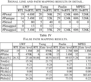
Table III shows the signal line and path mapping results in detail. Rows “#Ptotal”, “#Punique”, “#Stried”, “#Smapped” and “#Pmapped” show the total number of RTL paths, the number of paths uniquely identified with the I/O mapping information, the number of RTL signal lines targeted by signal line mapping, the number of RTL signal lines mapped, i.e., the gate level nets that are functionally equivalent to the bit-sliced RTL signal lines found, and the number of the RTL paths mapped. Columns “RTL” and “bsRTL” under each circuit name mean bundled RTL and bit-sliced RTL, respectively. Thanks to Definition 3 (unique identification of path), most of the RTL paths were able to be mapped only by using I/O mapping information or CPU time was able to be saved. The proposed method achieved90.9% RTL path mapping ratio and92.8% bit-sliced RTL path mapping ratio, in average. Here, we discuss the paths that are not mapped. (Bit-sliced) RTL paths that were not able to be mapped to the gate level paths existed because the algorithm was not able to find any signal line needed for path mapping, i.e., there existed no functionally equivalent net in the gate level circuits.
Table IV shows the result of RTL false path mapping and the time required for this mapping. Rows “#Ptotal”,
“#Pfalse”, “Ratio”, “Total”, “Unique”, “Ravi”, “FEchk”,
Table III
SIGNAL LINE AND PATH MAPPING RESULTS IN DETAIL.
LWF Tseng Paulin MPEG
RTL bsRTL RTL bsRTL RTL bsRTL RTL bsRTL
#Ptotal 19 4.6M 20 36K 29 124K 606 326K
#Punique 14 3.4M 18 32K 29 124K 606 326K
#Stried 5 80 5 40 0 0 0 0
#Smapped 0 13 0 12 - - - -
#Pmapped 14 3.4M 18 35K 29 124K 606 326K Table IV
FALSE PATH MAPPING RESULTS.
LWF Tseng Paulin MPEG
RTL Gate level RTL Gate level RTL Gate level RTL Gate level
#Ptotal 19 1.8M 20 856K 29 2.3M 606 1.8M
#Pfalse 5 470K 6 419K 13 1.6M 32 16
Ratio[%] 26.32 25.48 30.00 48.91 44.83 69.83 5.28 0.00
Total[s] 15.36 21.73 0.27 1.72
Unique[s] 0.21 0.24 0.27 1.72
Ravi[s] 15.15 17.07 0.00 0.00
FEchk[s] 0.00 4.42 0.00 0.00
Pwhole[s] 93.21 37.21 103.39 303.65
Pfalse[s] 24.26 19.07 73.53 0.22
“Pwhole” and “Pfalse” show the total number of paths, the number of false paths, the ratio of #Pfalse to #Ptotal, the total time required for false path mapping, the time required for finding candidates of functionally equivalent signal lines, the time required for equivalence checking, the time required for enumerating the whole paths in the gate level circuit and the time required for enumerating the false paths mapped, respectively. Columns “RTL” and “Gate level” under each circuit name mean the number of paths in RTL and the ones in gate level, respectively. Many gate level false paths were available with our proposed path mapping method in practical time without considering MIP-LS.
On the other hand, a sequential ATPG algorithm can identify false paths at gate level. However, sequential ATPG tools cannot identify them in a practical amount of time. For example, as reported in [6], TetraMax took about 50 hours to identify 10,000 false paths of Paulin. Since the RTL false path identification method proposed in [6] and our path mapping method took less than 1 second for several circuits, our high level identification approach is very effective.
Table V shows false path mapping results in detail. Rows
“#Pfalse”, “#Punique”, “#Stried” and “#Smapped” show the number of RTL false paths, the number of paths uniquely identified with the I/O mapping information, the number of bit-sliced RTL signal lines targeted by signal line mapping, and the number of bit-sliced RTL signal lines mapped, respectively. Therefore, we can say that the proposed method finds almost all gate level false paths corresponding to the given RTL false paths.
VI. CONCLUSIONS
Establishing correspondence between an RTL circuit and its synthesized gate level circuit is important for high level testing approaches. In this paper, we proposed a method to establish correspondence between a set of RTL paths and gate level paths without restricting logic synthesis. To the
Table V
DETAILS OF THE FALSE PATH MAPPING. LWF Tseng Paulin MPEG
#Pfalse 5 6 13 32
#Punique 4 5 13 32
#Stried 32 16 0 0
#Smapped 0 7 - -
best of our knowledge, this is the first work that tackles RTL to gate level path mapping. Furthermore, we showed that RTL false paths identified by [6] can be mapped to gate level false paths with our proposed method. In our experiments, the proposed path mapping method was utilized as a false path mapping procedure, and many false paths were able to be found in a circuit synthesized with an arbitrary logic synthesis by using our proposed path mapping method.
ACKNOWLEDGMENTS
The authors would like to thank Profs. Michiko Inoue and Tomokazu Yoneda of Nara Institute of Science and Technology and Yuki Yoshikawa of Hiroshima City Univer- sity for valuable discussion and cooperation. This work was supported in part by Semiconductor Technology Academic Research Center (STARC) under the Research Project and in part by Japan Society for the Promotion of Science (JSPS) under Grants-in-Aid for Scientific Research (B) (No. 20300018).
REFERENCES
[1] K. T. Cheng and H. C. Chen, “Classification and identification of nonrobust untestable path delay faults,” IEEE Trans. on CAD, vol. 15, no. 8, pp. 845–853, Aug. 1996.
[2] S. Kajihara, K. Kinoshita, I. Pomeranz, and S. Reddy, “A method for identifying robust dependent and functionally unsensitizable paths,” in International Conference on VLSI Design, 1997, pp. 82–87.
[3] S. M. Reddy, S. Kajihara, and I. Pomeranz, “An efficient method to identify untestable path delay faults,” in Asian Test Symposium, 2001, pp. 233–238.
[4] A. Krsti´c, S. T. Chakradhar, and K.-T. T. Cheng, “Testable path delay fault cover for sequential circuits,” in European Design and Test Conference, 1996, pp. 220–226.
[5] R. Tekumalla and P. Menon, “Identifying redundant path delay faults in sequential circuits,” in International Conference VLSI Design, 1996, pp. 406–411.
[6] Y. Yoshikawa, S. Ohtake, and H. Fujiwara, “False path identifi- cation using RTL information and its application to over-testing reduction for delay faults,” in Asian Test Symposium, 2007, pp. 65–68.
[7] S. Ravi, I. Ghosh, V. Boppana, and N. K. Jha, “Fault-diagnosis- based technique for establishing RTL and gate-level correspon- dences,” IEEE Trans. on CAD, vol. 20, no. 12, pp. 1414–1425, 2001.
[8] H. Iwata, S. Ohtake, and H. Fujiwara, “An approach to RTL false path mapping using uniqueness of paths,” Nara Institute of Science and Technology(NAIST), Tech. Rep. 2009004, 2009.
[9] Y. Yoshikawa, S. Ohtake, T. Inoue, and H. Fujiwara, “A synthesis method to alleviate over-testing of delay faults based on RTL don’t care path identification,” in IEEE VLSI Test Symposium, May. 2009, pp. 71–76.