A New Scan Design Technique Based on Pre-Synthesis Thru Functions
Chia Yee Ooi* and Hideo Fujiwara Graduate School of Information Science Nara Institute of Science and Technology
Kansai Science City 630-0192 Japan
E-mail: [email protected], [email protected]
Abstract
VLSI design has moved from bottom-up design approach to top-down design methodology with the aid of advanced Computer-Aided Design (CAD) technology. This paper introduces a new scan design technique as a design-for-test (DFT) method for sequential circuits by exploiting the information of thru functions available at high-level description of the circuit. This DFT method reduces the number of flip-flops to be converted into scan flip-flops because some existing thru functions allow the flip-flops to be controllable from primary inputs or observable at primary outputs or both. Moreover, the DFT method can be applied to both structural RT-level circuits and gate-level circuits. The paper also presents a test generation procedure for the augmented sequential circuits using a combinational ATPG tool. The experimental results show the comparison of our DFT method with conventional scan techniques in terms of hardware overhead, test generation time, fault coverage, fault efficiency and test application time. 1. Introduction
Design-for-testability (DFT) method is important to reduce the complexity of the test generation for sequential circuits. Since the test generation of a sequential circuit augmented by full scan technique can be reduced into the combinational test generation, the full scan technique is very popular. However, full scan technique requires all the flip-flops of a circuit to be augmented into scan flip-flops. ∗This results in large area overhead. Another disadvantage of the full scan technique is high test application time, which is resulted from the shifting of test vectors through the
∗Chia Yee Ooi is with Universiti Teknologi Malaysia and she is working on her Ph.D. at Nara Institute of Science and Technology.
scan chain.
In order to reduce the hardware area overhead, the number of flip-flops to be converted into scan flip-flops should be reduced. To achieve the objective, several partial scan techniques have been introduced. Among all, the partial scan technique, which breaks the minimum feedback loops [1], succeeds in reducing the number of scan flip-flops. This is then further reduced by cost-free scan [2] that establishes paths in the scan chain using existing logic and thus reduces the area overhead. Orthogonal scan [3] and partially strong testability method [4] are among other scan techniques but they are applicable in data path only. Besides DFT method, some works have introduced synthesis-for-testability (SFT) methods to augment a given design into easily testable based on the information obtained at high-level description [7,8,9,10].
H-scan [5, 6] utilizes the existing paths between registers, which consist of a series of multiplexers, to reduce the area overhead in the scan technique. The authors of [5] claimed that H-scan is applicable to a controller part as well as a data path part. In H-scan technique, some extra gates are added to the logic of the existing path so that signals transfer between the registers is enabled by a new input independent on the signals from the controller. In this paper, we introduce a new scan technique called Dependency-scan (abbrev. D-scan) technique that further reduces the area overhead. Similar to H-scan technique, D-scan utilizes the existing paths between two registers. Besides the exploitation of the existing paths, we also manipulate the information of the registers or the input signals, on which the existing paths are dependent to enable the signals transfer through the paths. This information can be obtained from the behavioral description of a design. Therefore, extra gates are not needed to enable the signals transfer for some existing paths. This can reduce the area overhead of the augmented circuit. 15th IEEE Asian Test Symposium (ATS'06), pp. 163-168, November 2006.
D-scan technique can be applied to any sequential circuit at gate-level and RT-level.
In Section 2, we define the extended connectivity graph based on the connectivity graph defined in [5] to show the thru functions available in the original design or simply pre-synthesis thru functions. Extended from the connectivity graph in H-scan technique, the graph contains extra information of the signals that activates the pre-synthesis thru functions. In Section 3, we introduce the new scan technique by exploiting the information of the pre-synthesis. In Section 4, we describe a test generation procedure for the sequential circuits augmented by the scan technique where the combinational ATPG tool is used. In Section 5, we present the experimental results of our DFT method. We also compare our method with full scan technique and a partial scan technique in terms of area overhead, pin overhead, test generation time, fault coverage, fault efficiency, and test application time in Section 5.
2. Preliminary
This section first briefly reviews the connectivity graph and introduces an extension of the connectivity graph called extended connectivity graph. Prior to the definition of extended connectivity graph, we define thru function, which is a logic function that allows signal transfer from its input to its output.
Definition 1: Thru function t is a logic that transfers the signals from the input of the thru function to the output. The output signals are the same with the input signals if the thru function is active. Note that the bit width of the input and output are equal.
Figure 1 shows two examples of the thru function. Two thru functions are independent if they cannot be active at the same time. t1 and t2 in Figure 1(b) are independent. Note that the multiplexing logic in a scan flip-flop is a kind of thru functions.
Figure 1. Thru functions.
Connectivity graph consists of a set of all paths for a given circuit that go through only multiplexers. Each vertex represents a register, input or output while each arc represents a path that goes through a series of multiplexers. We define extended connectivity graph, which is extended from the connectivity graph. Different from connectivity graph, each arc is a path that goes through a thru function and its label is the signals that activate the thru function.
Definition 2: Extended connectivity graph of a sequential circuit is a directed graph G=(V,A,t) that has
the following properties.
1. vi∈V represents a register (resp. a flip-flop), an input port (resp. input) or an output port (resp. output) of the sequential circuit, where a register is a group of flip-flops (resp. an input port is a group of inputs and an output port is a group of outputs) that connect to the same component or/and are connected from the same component;
2. (vi, vj)∈A denotes an arc if there exists a combinational path from the register (resp. flip-flop) corresponding to vi to the register (resp. flip-flop) corresponding to vj.
3. t:AÆT∪{1} (T is a set of thru functions {t0, t1, …, ti}) where t(a)≠φ contains the signal values of a set of vertices that activate the thru function, in which each vertex corresponds to a register (resp. flip-flop) or an input port (resp. input). If t(a)=1 (identity thru function), the signal values are transferred from the source vertex of arc a to the sink vertex of arc a through a wire logic (not gate logic) directly without assignment of any signal values.
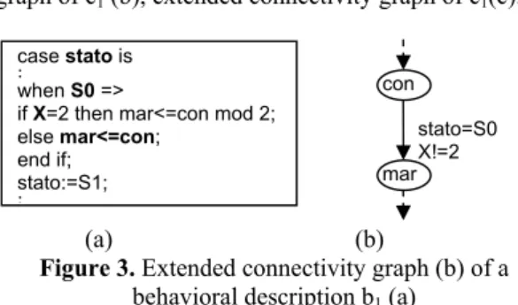
(a) (b) (c) Figure2.Subcircuit c1 at RT-level(a), connectivity graph of c1 (b), extended connectivity graph of c1(c).
(a) (b)
Figure 3. Extended connectivity graph (b) of a behavioral description b1 (a)
Figure 2 shows the extraction of the information of thru functions from RT-level description into a connectivity graph and an extended connectivity graph. Figure 3 illustrates the extraction of the thru function information from a behavioral description to the extended connectivity graph. No connectivity graph can be built from the behavioral description because the information of the existence of a series of multiplexers cannot be obtained. An extended connectivity graph of a given circuit at gate-level can be constructed provided either it RT-level description or behavioral description is available. The thru function
0 1
0 1 R2 a
b
a=1
b R1
R3
a R1 R2
R3 R2
R1
R3
stato=S0 X!=2 con
mar case stato is
. .
when S0 =>
if X=2 then mar<=con mod 2; else mar<=con;
end if; stato:=S1; ..
t1
t1
t1
t2
m1 m2 m3 I1
I2
I3
O1
I1
I2
I3
O1
m4=m1+m2
m1 m2 m3
m4=m1
=m2
(a) (b)
that is extracted from the high-level description is called pre-synthesis thru function.
3. Design-For-Testability Method
We introduce a new scan approach called Dependency-scan (abbrev. D-scan). A scan path resulted from D-scan technique is called D-scan path. The following text discusses the case of gate-level sequential circuits where each vertex of its extended connectivity graph represents a one-bit primary input or one-bit primary output or flip-flop. The discussion for the case of RT-level can be derived similarly. Definition 3: A D-scan path in a sequential circuit S is a path which satisfies the following conditions. 1. The path is corresponding to a path in the extended
connectivity graph of S that starts from a vertex corresponding to an input of S and ends at a vertex corresponding to an output of S; and
2. If a vertex vi is on the path, any signal values of the flip-flop or input that corresponds to vertex vi
is not a label of any arc on the path.
Condition 1 in Definition 3 means a D-scan path has a scan-in input which is a primary input and a scan-out input which is a primary output. Also, the signals are transferable from a flip-flop (or scan-in input) to another flip-flop (or scan-out output). Condition 2 in Definition 3 makes sure that the signals transfer from one flip-flop (or scan-in input) to the next flip-flop (or scan-out output) is not enabled by any signal of the flip-flop that is being transferred through the path. Definition 4: Let SP1 and SP2 denote any pair of the D-scan paths in a sequential circuit S. The sequential circuit S is a D-scan design if the following conditions are satisfied.
1. There exists a set of D-scan paths that covers the vertices corresponding to all the flip-flops in the circuit;
2. SP1 and SP2 must have disjoint vertices except the vertices that correspond to the scan-out output; and 3. If one of the thru functions on SP1 depends on a flip-flop or input corresponding to vertex vi in SP2 to become active, SP2 does not depend on any flip-flop corresponding to a vertex on SP1 to become active.
Condition 1 in Definition 4 says that each D-scan path is responsible to the justification of a set of flip-flops which is disjoint from the set of flip-flops on different D-scan path in the sequential circuit. But, the signals of different flip-flops can be observed at the same scan-out output. A scan path is said to be active if all the thru functions on the path are activated. Condition 2 in Definition 4 requires that two D-scan paths cannot depend on each other to become active.
One of the scan paths have to be activated independently on the other scan path so that the latter can be activated by the signals of some flip-flops on the former after it becomes active.
An arbitrary sequential circuit is augmented by adding minimum thru functions to the circuit so that the circuit becomes a D-scan design, as defined in Definition 4. Similarly, the technique can be done for partial scan where the set of D-scan paths stated in Definition 4 is required to cover only the vertices of minimum feedback vertex set. The following is the steps of D-scan technique for an arbitrary sequential circuit S in the case of full-scan.
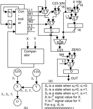
Figure 4. The greatest common divider (GCD) circuit (a) and its extended connectivity graph (b).
Step 1. Identify the flip-flops and inputs that activate a pre-synthesis thru functions. The set of flip-flops and inputs is denoted as G1.
Step 2. Construct the extended connectivity graph of S. The set of flip-flops and inputs corresponding to the vertices in the graph is denoted as G2.
Step 3. The remaining flip-flops are included in G1 (resp. G2) if the number of inputs in G1 (resp. G2) is more. This is to get shorter test application time.
L4 M2 L3 L2 L1
M1 0 1 0 1
0 1
0 1 0 1
X
Y
C23 ZERO
O 0 1 0 1
(a) OUT
L3 Compar-
ator X Y
M4 Con
- troll er s0
s1
C23 XIN 16
SUB
(b)
16 X YIN M3 L2
16
S0 is a state when s0=0, s1=0. S1 is a state when s0=0, s1=1. S3 is a state when s0=1, s1=1. Xi is ith signal value for X. Yi is ith signal value for Y. For e.g. X3 is
0000000000000011
XIN X S0
O test
YIN Y S0 test
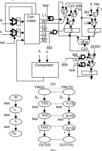
Figure 5. Extended connectivity graph after D-scan augmentation
XIN
X S0
O S3, Xk, Yl
YIN
Y S0
S1, Xi, Yj
Step 4. Add minimum new thru functions such that z the extended connectivity graph consists of the
vertices of all flip-flops,
z there exists a set of D-scan paths that cover the vertices of all flip-flops and
z all flip-flops on each D-scan are from either G1 or G2 but not both.
Note that the DFT method does not guarantee minimum test application time because our objective is to reduce area overhead. At most one multiplexer is added between two flip-flops during the DFT method. There are two methods to add a new thru function between two registers u and v.
1. Add a new multiplexer with a new input test as a select input where register u is connected to one of the data inputs of the multiplexer and the data output of the multiplexer is connected to the input of register v.
2. Add a new 2-input OR gate (resp. AND gate) with a new input test (resp. test ) and connect the output to the select input of the multiplexers so that data transfer from register u to v when test=1.
Method 2 is applicable if there is a series of multiplexers from register u to v. Else, Method 1 is used. Figure 4 shows GCD. Since s0 and s1 activates the existing thru functions, s0 and s1 are included in G1. Registers X and Y are included in G2 as showed in Figure 5. Figure 6 illustrates the resulting D-scan paths.
4. Test Generation Procedure
In this section, we discuss the test generation procedure for gate-level circuits where one vertex represents a flip-flop instead of a register. The discussion for the RTL circuits can be derived similarly. The procedure uses a combinational ATPG for the test generation. The test generation generates tests for all faults including the faults in the logic related to pre-synthesis thru functions. The way to check the post-synthesis thru functions is same as checking the shifting operation of the scan path in a full scan designed circuit, that is by the alternating one and zero sequences.
4.1. Time expansion model
Since we are using the existing logic in shifting operation, we use time expansion model to generate tests for the faults in the combinational kernel as well as the logic related to the shifting operation. The outputs of the flip-flops (resp. inputs of the flip-flops) of the scan path that does not have pre-synthesis thru functions are treated as inputs (outputs) in the time expansion model because the test patterns at the
flip-flops can be justified and observed through the scan path.
(a)
(b)
Figure 6. The augmented circuit under D-scan (a) and the set of D-scan paths (b).
Example 1. Figure 7 shows the registers and the kernel of GCD after DFT and Figure 8 shows the time expansion model for the GCD circuit in Figure 4. All D-scan paths operate the shifting process at different time. Let f denote a stuck-at fault in the combinational part of the GCD circuit. In justification phase, prior to T0, the D-scan path that consists of s0 and s1 justify the signal values at s0 and s1 that activate the pre-synthesis thru functions. From T0 to T2, flip-flop s0 and s1 with the signal values that activate the pre-synthesis thru functions are in hold mode so that D-scan path with the pre-synthesis thru functions can justify the signal values at registers X, Y and O that are needed to excite f at T5. X, Y and O are then in hold mode to allow s0 and s1 be justified the signal values that are needed to excite f at T5. The similar procedure is done for the propagation phase. The arrow in each duplicate of the combinational part is a pre-synthesis thru function.
Test generation on the time expansion model of a D-scan design is performed as follows.
O L4
L1 0 1
0 1
0 1 SUB
ZERO M3
L2
M4 L3 0 1
X C23 XIN
16
0 1 0 1
16 X YIN
Y
0 1 C23 Con-
troller M1 L2 L3 s0
s1
Comparator X Y
M2
0 1
0 1
SI
s0
test M3
test test
test test
SI
Y(0) s0
X(0) s1
O0
O(0)
OUT(0) OUT(15)
S0 S0
test
test test
test test
1 1
test
test
X(15)
O(15) Y(15) YIN(0) ………….YIN(15)
Step 1. Generate tests for the combinational equivalent of time expansion model using multiple fault modeling by a combinational ATPG tool.
Step 2. Convert the tests into the test sequence. The test generation of D-scan designed circuit is equivalent to the test generation of acyclic sequential circuits, which is at most the square of the combinational test generation complexity. This is stated in the following theorem followed by its proof.
Figure 7. Registers and the kernel of GCD.
Theorem 1. The combinational test generation algorithm on the time expansion model can identify redundancy and all testable faults.
Theorem 2. The test generation for D-scan designed circuits is at most the square of the combinational test generation complexity.
Proof: Given a D-scan designed circuit, the test generation model with 2D+1 time frames is generated where D is the total number of registers. By assuming D=O(n), where n is the size of the circuit, the size of the time expansion model is at most 2n2. Since the ATPG tool is used for test generation process, the test generation complexity is at most the square of the combinational test generation with size n.
5. Experimental Results
Experiment is conducted on ITC’99 benchmark circuits where the behavioral netlists and the gate-level
netlists are given. We extract the information of thru functions from the behavioral netlists. TetraMax is used to generate tests for the circuits in the experiment. Experiment is run on Sun Microsystems.
We compare the results with full scan circuits and partial scan circuits. The partial scan technique in this text means the scan technique that breaks the minimum flip-flops of the feedback in the circuit. Table 1 presents the characteristics of the benchmark circuits. Table 2 and 3 shows the area overhead and pin overhead, respectively. Table 4 shows the test generation time necessary in the benchmark circuits augmented by scan techniques and our DFT method. Table 5 shows the fault coverage as well as the fault efficiency where det. denotes detected faults and red. denotes redundant faults. Table 6 is the test application time needed. The last rows of Tables 2, 3, 4 and 6 show the average area overhead, pin overhead, test generation time and test application time, respectively.
Table 1. Characteristics of ITC99
IO pins
#FF s
Area
PI PO
Thru information B03 30 554 6 4 16 thru functions B04 66 1927 13 8 40 thru functions B07 49 1239 3 8 8 thru functions B08 21 516 11 4 8 thru function B09 28 557 3 1 1 thru functions B10 17 523 13 6 4 thru functions B11 31 1688 9 6 6 thru functions B12 121 3177 7 6 6 thru functions B13 53 1088 12 10 12 thru functions
Our method shows that less hardware area overhead resulted compared with conventional scan techniques. Moreover, the result shows shorter test application time in some cases where parallelism is possible. There is still room of improvement in minimizing test application time.
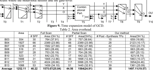
Figure 9. Time expansion model of GCD. Table 2. Area overhead.
Full Scan Partial Scan Our method
Area
# SFF Area (OH %) # SFF Area(OH%) # Post –Synthesis TFs Area(OH %)
B03 554 30 764 (37.91) 29 757 (36.64) 15 659 (18.95)
B04 1927 66 2389 (23.98) 66 2389 (23.98) 28 2123 (10.17)
B07 1239 49 1582 (27.68) 49 1582 (27.68) 42 1533 (23.73)
B08 516 21 663 (28.49) 21 663 (28.49) 21 663 (28.49)
B09 557 28 753 (35.19) 21 704 (26.39) 20 697 (25.13)
B10 523 17 642 (22.75) 17 642 (22.75) 14 621(18.74)
B11 1688 31 1905 (12.86) 30 1898 (12.44) 25 1863 (10.37)
B12 3177 121 4024 (26.66) 117 3996 (25.78) 111 3954(24.46)
B13 1088 53 1459 (34.10) 51 1445 (32.81) 39 1361 (25.09)
Average 1252.11 46.22 1575.67(25.84) 44.56 1564(24.91) 35 1497.11(19.57) s1
O YIN
Combinationa
l part OUTPUT
X Y O s1
s0
Combin ational Part. f
Y Y
X X
O O
s0
s1
s0
Y X YIN YIN
OUT
X
O OUT
T0 T1 T2 T3 T4 T5 T6 T7 T8 T9 T10
s0
s1 s0
s1
Y
Table 3. Pin overhead for ITC99
Partial Scan Our method I O Total I O Total
B03 3 1 4 4 0 4
B04 3 1 4 4 0 4
B07 3 1 4 4 0 4
B08 3 1 4 5 0 5
B09 3 1 4 5 0 5
B10 3 1 4 4 0 4
B11 3 1 4 4 0 4
B12 3 1 4 4 0 4
B13 3 1 4 4 0 4
Average 3 1 4 4.5 0 4.5
Table 4. Test generation time(seconds) for ITC99
Original Full Scan
Partial Scan
Our method
B03 942.73 0.01 0.02 10.53
B04 1823.25 0.53 1.67 8.72
B07 12101.68 0.01 0.12 6.15
B08 218.19 0.01 0.05 0.09
B09 639.09 0.01 0.09 0.19
B10 393.29 0.01 0.04 0.15
B11 9608.75 0.04 0.37 310.40
B12 29409.50 0.05 0.65 5.70
B13 2474.20 0.01 0.06 0.25
Average 6401.19 0.08 0.34 38.02
Table 5. Fault efficiency (Fault coverage)(%) for ITC99
Our method Original Full Scan Partial Scan
Det Red total FE(FC) B03 72.04 100 (100 ) 100 (100 ) 1262 0 1262 100(100) B04 86.16 100 (98.79) 100 (98.79) 4910 50 4960 100 (98.99) B07 3.45 100 (99.76) 100 (99.76) 3618 6 3624 100 (99.83) B08 88.58 100 (100 ) 100 ( 100) 1448 0 1448 100(100) B09 87.66 100 (100 ) 100 (100 ) 1496 0 1496 100(100) B10 90.65 100 (100 ) 100 (100 ) 1550 0 1550 100(100) B11 55.99 100 (96.29) 100 (96.29) 4857 161 5018 100 (96.79 ) B12 17.12 100 (100 ) 100 (100 ) 9420 0 9420 100(100) B13 30.48 100 (95.83) 100 (95.83) 3000 80 3080 100 (97.40 )
Table 6. Test application time(clock cycles) for ITC99
Full Scan Partial Scan Our method
B03 1110 1711 1176
B04 8712 15576 2700
B07 3479 5488 8330
B08 1113 1869 904
B09 1344 1974 4977
B10 1122 1700 1310
B11 3875 6240 1890
B12 26983 53360 28800
B13 2862 4896 1872
Average 5622.22 10312.67 5773.22
6. Conclusion
A new scan technique called D-scan technique has been introduced in this paper based on the information of pre-synthesis thru function extracted from the high-level description. Our method shows that less hardware area overhead resulted compared with scan techniques. Moreover, the result shows shorter test application time in some cases where parallelism is possible. There is still room of improvement in minimizing test application time.
REFERENCES
[1] D.H. Lee and S.M. Reddy, “On Determining Scan Flip-Flops in Partial-Scan Designs,” Proc. Int. Conf. on Computer-Aided Design, pp. 322—325, Nov. 1990. [2] C. Lin, M. Marek-Sadowska, M.T. Lee and K. Chen, “Cost-Free Scan: A Low-Overhead Scan Path Design,” IEEE Trans. on CAD of Integrated Circuits and System, Vol. 17, No. 19, pp. 852-861, Sept. 1998. [3] R.B. Norwood and E.J. McCluskey, “Orthogonal
Scan: Low Overhead Scan for Data Paths,” Proc. International Test Conference, pp. 659-668, Nov. 1996.
[4] H. Iwata, T. Yoneda, S. Ohtake and H. Fujiwara,
“A DFT Method for RTL Data Paths Based on Partially Strong Testability to Guarantee Complete Fault Efficiency,” Proc. IEEE 14th Asian Test Symposium (ATS’05), pp. 306-311, Dec. 2005.
[5] S. Bhattacharya and S. Dey, “H-Scan: A High Level Alternative to Full-Scan Testing With Reduced Area and Test Application Overheads,” Proc. IEEE 14th VLSI Test Symposium (VTS’96), pp. 74-80, 1996. [6] T. Asaka, S. Bhattacharya, S. Dey and M. Yoshida,
“H-Scan+: A Practical Low-Overhead RTL Design-for-Testability Technique for Industrial Designs,” Proc. International Test Conference, pp. 265-274, 1997.
[7] M. S. Abadir and M. A. Breuer, “A Knowledge Based System for Designing Testable VLSI Chips,” IEEE Design & Test of Computers, vol. 2, no. 4, pp. 56—68, August 1985.
[8] V. D. Agrawal and K. T. Cheng, “Finite State Machine Synthesis with Embedded Test Function,” Journal Electronic Testing: Theory and Applications (JETTA), vol. 1, no. 3, pp. 221—228, 1990.
[9] S. Kanjilal, S. T. Chakradhar and V. D. Agrawal,
“Test Function Embedding Algorithms with Application to Interconnected Finite State Machines,” IEEE Trans. CAD, vol. 14, pp. 1115—1127.
[10] H. Fujiwara, Y. Nagao, T. Sasao, and K. Kinoshita, "Easily testable sequential machines with extra inputs," IEEE Trans. on Computers, Vol. C-24, No. 8, pp. 821-826, Aug. 1975.