Fault Dependent/Independent Two-Pattern Test Generation Methods for State
Observable FSMs
Toshinori Hosokawa† Ryoichi Inoue†† and Hideo Fujiwara‡
†College of Industrial Technology, Nihon University 1-2-1, Izumicho, Narashino, Chiba 275-8575, Japan
††Graduate School of Industrial Technology, Nihon University 1-2-1, Izumicho, Narashino, Chiba 275-8575, Japan
‡Graduate School of Information Science, Nara Institute of Science and Technology (NAIST) 8916-5, Takayama, Ikoma, Nara 630-0192, Japan
E-mail: † [email protected], ††[email protected],‡[email protected]
Abstract
Scan testing is one of the most popular test methods for VLSIs. However, since scan testing is not based on the function of the circuit, but rather its structure, this method is considered to be a form of over testing or under testing. Hence, a yield loss of VLSIs, as well as outflow of defective VLSIs into the market, may occur. It is important to test VLSIs using the given function. Since the functional specifications are described explicitly in the FSMs, high test quality is expected by performing logical testing and timing testing. This paper proposes two test generation methods, a fault-independent two-pattern test generation method and a fault-dependent two-pattern test generation method, for timing testing in state- observable FSMs in order to reduce the yield loss while improving the test quality over scan testing. The experimental results for MCNC'91 benchmark circuits show that the use of the proposed method is effective for the improvement of one-state transition coverage and two-state transition coverage.
keywords: State-observable FSMs, Over testing, Fault-dependent/independent two-pattern test generation, Two-state transition coverage
1. Introduction
In recent years, Very Large Scale Integrated circuit (VLSI) testing has become increasingly important because the number of gates on VLSIs is rapidly increasing and their complexity is growing with advances in semiconductor technology. Currently, scan testing for the stuck-at fault model [1, 2] is one of the most popular test methods for VLSIs. However, it has been reported that scan testing for the stuck-at fault model may not detect defective VLSIs [4], and delay testing [3] and at-speed functional testing can effectively improve test quality.
As mentioned above, scan testing is currently the most popular test method. Scan testing is based on the structure of the circuit rather than its function. In scan testing, the states of the circuits are transferred to invalid states by shift operation during the testing in order to detect faults. This method is considered to be a form of over testing and a yield loss of VLSIs may occur. Scan testing also detects faults by the operation of a combinational circuit part, shifting-in, and shifting-out. Hence, faults are not detected by performing sequential operations of circuits. This testing is considered to be a form of under testing. Therefore, the test quality deteriorates, and outflow of defective VLSIs into the market may occur.
VLSI design methodologies employing hardware description languages have recently been adopted to reduce VLSI design time. VLSIs are designed at the Register Transfer Level (RTL), and RTL circuits consist of a data path part and a controller part. The data path contains a hardware element (e.g., registers, multiplexers, and operational modules) and signal lines. The controller is represented by a finite state machine (FSM). A non-scan-based Design For Testability (DFT) method of data path parts is proposed in [5], whereas a non-scan-based DFT method for controller parts is proposed in [6]. At- speed testing is easily applicable, and test patterns for a stuck-at fault model are completely generated by non-scan-based DFT methods. As mentioned above, if at-speed functional testing and/or delay testing are applied to VLSIs with a non-scan-based DFT, the test quality can be further improved. As for the FSM, which is the controller part of a RTL circuit, the circuit specification is described explicitly. Thus, it is expected that the test quality becomes high by performing a logical test and a timing test under the constraints of the circuit specifications. It was reported in [7] that state-observable and completely
IEEE 7th Workshop on RTL and High Level Testing (WRTLT'06), pp. 13-18, November, 2006.
specified FSMs are thoroughly logically tested by performing all of the state transitions. Thus, complete at-speed logical testing can be applied to FSMs having states that are made observable by performing all state transitions at-speed. Complete timing testing can be also applied by performing all pairs of state transitions at-speed.
In [11], two test generation methods, a fault- independent one-pattern test generation method and a fault-dependent one-pattern test generation method were proposed for logical testing in state-observable FSMs. One-state transition coverage [11] was also proposed as the measure of test quality for logical testing. The experimental results for MCNC’91 benchmark circuits [9] show that the use of the method reduced the area while the one-state transition coverage was increased compared with the conventional non-scan test method [6] for state- observable FSMs.
This paper proposes two test generation methods, a fault-independent two-pattern test generation method and a fault-dependent two-pattern test generation method for state-observable FSMs in order to reduce the yield loss caused by over testing, while improving the test quality over that of scan testing. This paper also proposes two-state transition coverage as measure of test quality for timing testing. Two-state transition coverage is defined as the ratio of the number of state transition pairs executed by a test sequence to the total number of continuous state transition pairs.
This paper is organized as follows. In Section 2, the definition of state-observable FSMs and a test method for state-observable are described. In Section 3, the optimization problems for both fault- independent two-pattern test and fault-dependent two-pattern test are formulated for state-observable FSMs, and their test generation methods are proposed. The proposed methods are applied to MCNC’91 FSM benchmarks [9] in Section 4, and the experimental results are presented. Furthermore, the ratios of over testing for single stuck-at fault scan testing and path delay fault scan testing based on the broadside approach are evaluated. Finally, Section 5 concludes the paper and discusses future research possibilities.
2. State-observable FSMs (Definition 1: State-observable FSMs)
When an initial state can be identified by observing an output sequence without being dependent on an input sequence, the FSM is said to be state-observable. More specifically, when an initial state can be identified by observing an output sequence of k length, the FSM is said to be k state- observable.
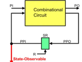
The DFT transformed an FSM to a one-state observable FSM by making the outputs of the status registers in the FSM observable. In this paper, a one- state observable FSM is hereinafter referred to simply as a state-observable FSM. A synchronous sequential circuit is synthesized from the FSM by logic synthesis. Figure 1 shows the logic circuit model that corresponds to the FSM after logic synthesis. Because the pseudo primary inputs (PPI), which are the outputs of the status registers, are observable in this figure, the PPI connect with the primary output. Here, PI, PO, SR, PPI, PPO, and R denote the primary inputs, primary outputs, status registers, pseudo primary inputs (outputs of the status registers), pseudo primary outputs (inputs of the status registers), and a reset input, respectively.
In the test for state-observable FSMs, the PI value is applied to a state-observable FSM, the state is then transferred from the current state to the next state, and the resulting PPI and PO values are observed. A series of these procedures is referred to as a test for state-observable FSMs.
The FSM has a completely specified FSM [8], in which the next state and the output are specified for all of the inputs of each state, and an incompletely specified FSM [8], in which the next state and the output are not specified for all of the inputs of each state. In this paper, in the incompletely specified FSMs, state transitions that are not specified are assumed to be the same as either of the state transitions that are specified.
Fig. 1 Logic model for a state-observable FSM
Combinational Circuit
State-Observable
PO PI
SR
PPI PPO
R
3. Two-Pattern Test Generation Method for State-observable FSMs
Timing testing is performed to test any detectable fault models by a two-pattern test. An FSM timing test generation graph is defined as the model by which to generate a two-pattern test for timing testing in state-observable FSMs, and two-state transition coverage is proposed as the measure of test quality for timing testing.
(Definition 2: FSM timing test generation graph) An FSM timing test generation graph is a directed graph G(V, E, s, d, t), where a vertex v ∈ V denotes a state transition. Each vertex has a label s: V
→ A (A = {PPI1PPI2… PPIm}, PPI1, PPI2,…, PPIm
∈ {0, 1}, where m denotes the number of status registers), a label d: V → A (A = {PPI1PPI2…PPIm}, PPI1, PPI2,…, PPIm∈ {0, 1}, and a label t: V → B (B = {PI1PI2…PIn}, PI1, PI2, …, PIn∈ {0, 1}, where n denotes the number of primary inputs). The label s indicates the source state of the state transition, the label d indicates the destination state of the state transition, and the label t indicates input values for the state transition. For any vertices u, v ∈ V, an edge (u, v) ∈ E denotes that the destination state in u is the same as the source state in v. The edge (u, v) represents a continuous state transition pair.
(Definition 3: Two-state transition coverage) Two-state transition coverage is defined as the ratio of the number of continuous state transition pairs executed by a test sequence to the total number of continuous state transition pairs. When continuous state transition pairs are executed by a test sequence, the continuous state transition pairs are said to be covered by the test sequence. In this paper, only continuous state transition pairs specified in an FSM are used to calculate the two-state transition coverage. Two-state transition coverage is used as the measure of the test quality for timing testing.
3.1 Fault-independent Test Generation Method for Timing Testing
The following problem is formulated for a fault- independent test generation method of timing testing for state-observable FSMs.
(Formulation 2a)
Input: a state-observable FSM.
Output: a test sequence such that the two-state transition coverage is 100%. (All continuous state transition pairs in the FSM are performed.) Optimization: minimization of the test length. The test generation for Formulation 2a does not use ATPG for a specific fault model. An FSM timing test generation graph is generated from the state- observable FSM and searches the path such that all of the edges are traversed at least once. If the path length is minimized, then the test length is also minimized. This test sequence can perform a timing test on a state-observable FSM completely.
3.2 Fault-dependent Test Generation Method for Timing Testing
In this paper, a non-robust testable path delay fault model is considered as a representative of detectable fault models by timing testing. A non-robust testable path delay fault model is hereinafter referred to simply as a path delay fault. The following problem is formulated for a test generation method of path delay faults for state-observable FSMs.
(Definition 4: Detectable path delay faults on the transition between valid states)
The transition between valid states refers to performing state transitions between valid states in state-observable FSMs. After a transition between valid states, path delay faults detected by performing a continuous state transition are defined as detectable delay faults on the transition between valid states. (Formulation 2b)
Input:
- a state-observable FSM.
- a two-pattern test set that can detect all detectable path delay faults on the transition between valid states.
Output: a test sequence for a state-observable FSM such that all detectable path delay faults on the transition between valid states are detected. Optimization: minimization of the test length.
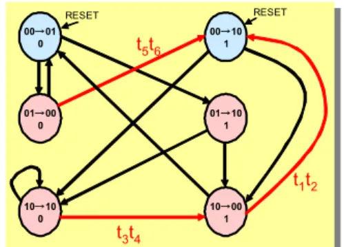
Fig. 2 Example of an FSM (three states)
S0 S1
S2 0 0
1 0
1 1 RESET
Fig. 3 FSM timing test generation graph for path delay fault testing
After logic synthesis, a time expansion model [10] for two time frames is generated from a synthesized sequential circuit. The valid states are assigned to the PPI values as constraints. A constrained ATPG for path delay faults is performed for the time expansion model, and a two-pattern test set is generated. An FSM timing test generation graph is then generated and two-pattern tests are assigned to the corresponding edges of an FSM timing test generation graph. Finally, paths are searched on the FSM timing test generation graph such that all of the edges where two-pattern tests are assigned are traversed at least once. If the path length is minimized, then the test length is also minimized. Example: Figure 3 shows an FSM timing test generation graph that is generated from the state- observable FSM shown in Fig. 2 and a two-pattern test set, which can detect all detectable path delay faults on the transition between valid states for a time expansion model with two time frames. The state 00 is assigned to S0, the state 01 is assigned to S1, and the state 10 is assigned to S2. Each two-pattern test is assigned to the corresponding edge in this graph. For example, t5t6 is assigned to the edge that represents the continuous state transition pair, which is the state transition from the valid state 01 through the input value 0 to the valid state 00, and the state transition from the valid state 00 through the input value 1 to the valid state 10. When the test sequence (0, 0, 1, 0, 1, 1) is applied to the FSM shown in Fig. 2 on the current state S0 (reset state), the five state transition pairs are covered in the FSM timing test generation graph shown in Fig.3. Thus, the two-state transition coverage is 41.7% (5/12).
4. Experimental Results
The test generation methods for Formulations 2a and 2b were implemented and were applied to MCNC’91 benchmark circuits [9].
The platform used for the experiments is as follows:
CPU: Pentium 4 Frequency: 3 GHz Memory: 2 Gbytes
The characteristics of MCNC’91 benchmark circuits are shown in Table 1. In this figure, Circuit,
#Node, #PI, #PO, #Reg, #Edge, and Area denote the circuit name of the FSM, the number of states, the number of primary inputs, the number of primary outputs, the number of status registers, the number of state transitions, and the area of synthesized sequential circuit that was calculated based on the standard library for logic synthesis, respectively. In these experiments, the FSMs were made state- observable by DFT, and two test generations were performed for state-observable FSMs. The logic syntheses for the FSMs were performed using a Synopsys Design Compiler® and the test generations for the combinational circuit part were performed using Synopsys TetraMax®.
Table 2 shows the experimental results of the test generation methods for timing testing proposed in this paper. In Table 2, 2a denotes the fault- independent test generation method for timing testing, and 2b denotes the fault-dependent test generation method for timing testing. In Tables 2, Circuit, TL, SFC, 1STC, PSC, 2STC, and CPU time denote the circuit name of the FSM, the test length, the fault coverage of detectable stuck-at faults on valid states, the one-state transition coverage, the fault coverage of detectable path delay faults on transition between valid states, two-state transition coverage, and the time for the test generation, respectively.
For 2a, since both the one-state transition coverage and the two-state transition coverage are 100%, the logical fault model including stuck-at faults and the timing fault model including path delay faults can be completely tested. 2a is applicable to FSMs that have less than 1,000 state transitions with reasonable CPU time and test length (maximum: 6,512). However, the test lengths for FSMs that have many state transitions drastically increase. For 2b, the one-state transition coverage was higher than that for stuck-at fault dependent test generation shown in [11]. In this paper,
00→ 01 0
00→ 10 1
01→ 00 0
01→ 10 1
10→ 10 0
10→ 00 1
RESET RESET
t1t2
t3t4 t5t6
this stuck-at fault test generation is said to 1b. However, the fault coverage for detectable stuck-at faults on valid states was an average of 93.7% of that for 1b. 2b could not completely test stuck-at faults, and the two-state transition coverage was an average of 63.6% higher than for 1b.
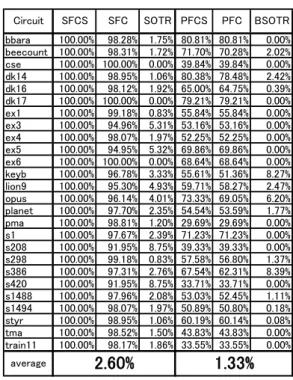
Table 3 shows the experimental results for evaluation of the ratios of over testing for stuck-at fault scan testing and path delay fault scan testing based on the broadside approach. In Table 3, Circuit denotes the circuit name of the FSM, SFCS denotes the fault coverage of stuck-at fault scan testing, SFC denotes the stuck-at fault coverage by 1b, SOTR denotes the ratios of over testing for stuck-at fault scan testing, PFCS denotes the fault coverage of path delay fault scan testing based on the broadside approach, PFC denotes the path delay fault coverage by 2b, and BSOTR denotes the ratios of over testing for path delay fault scan testing based on the broadside approach. SOTR and BSOTR are expressed by the following equations:
) 1 ...(
(%) SFC
SFC SOTR =SFCS−
) 2 ...(
(%) PFC
PFC
BSOTR =PFCS−
Table 3 shows that the average faults of 2.6% are over tested on stuck-at fault scan testing. In particular, stuck-at faults of 5% to 8% are over tested for ex3, ex5, s208, and s420. The number of one-pattern tests for the combinational circuit part is increased by 16% to 26%. In addition, Table 3 shows that the average faults of 1.3% are over tested on path delay fault testing based on the broadside approach. In particular, path delay faults of 6% to 8% are over-tested for keyb, opus, and s386. The number of two-pattern tests for a combinational circuit part increased by 14% to 37%.
5. Conclusion
This paper proposed both a fault-independent two- pattern test generation method and a fault-dependent two-pattern test generation method for state observable FSMs. This paper also proposed two-state transition coverage as the measure of test quality for timing testing. The quality and cost of timing testing for proposed test generation methods was evaluated for MCNC’91 benchmark circuits. Moreover, the ratios of over testing for stuck-at and path delay scan testing were evaluated.
Future studies will include an analysis of the relationship among one(two)-state transition coverage, fault coverage for various fault models, and a one(two)-pattern test set, and the proposal of a test generation method to maximize one(two)-state transition coverage under constraints such as test length and fault models, which must perform a complete test.
References
[1] H. Fujiwara, “Logic Testing and Design for Testability,” The MIT Press, 1985.
[2] M. Abramovici, M. A. Breuer, and A. D. Friedman, “Digital systems testing and testable design,” IEEE Press, 1995.
[3] A. Krstic, and K.-T. Cheng, “Delay Fault Testing for VLSI Circuits,” Kluwer Academic Publishers, 1998.
[4] P.C. Maxwell, R.C. Aitken, R. Kollitz, and A. C. Brown, “IDDQ and AC Scan: The War Against Unmodelled Defects,” Proc. of IEEE Int. Test Conf., pp.250-258, Oct., 1996.
[5] H. Wada, T. Masuzawa, K.K. Saluja, and H. Fujiwara, “Design for strong testability of RTL data paths to provide complete fault efficiency,” Proc. of 13th Int. Conf. on VLSI Design, pp.300-305, 2000.
[6] S. Ohtake, T. Masuzawa, and H. Fujiwara, "A non-scan approach to DFT for Controllers Achieving 100% Fault Efficiency," Journal of Electronic Testing: Theory and Applications (JETTA), Vol. 16, No. 5, pp.553-566, Oct. 2000. [7] H. Fujiwara, and K. Kinoshita, “Design of Diagnosable Sequential Machines Utilizing Extra Outputs,” IEEE Trans. on Computers, Vol. C-23, pp.138-145, Feb., 1974.
[8] T. Sasao, “Switching Theory for Logic Synthesis,” Kluwer Academic Pub., 1999. [9] S. Yang, "Logic synthesis and optimization
benchmarks user guide," Technical Report 1991-IWLS-UG-Saeyang, Microelectronics Center of North Carolina, 1999.
[10] T. Inoue, T. Hosokawa, T. Mihara,, and H. Fujiwara, “An optimal time expansion model based on combinational ATPG for RT level circuits”, IEEE Proc. Asian Test Symp., pp.190- 197 , Dec. 1998.
[11] T. Hosokawa, and H. Fujiwara, “A functional test method for state observable FSMs”, IEEE Workshop on RTL and High Level Testing, pp.123-130, July 2005.
Table 1 FSM benchmark characteristics Table 3 Experimental results of the over testing
Table 2 Experimental results of the test generation methods for timing testing
i
i
i i # # I # # g # g
. % . % . % . % . % . %
. % . % . % . % . % . %
. % . % . % . % . % . %
. % . % . % . % . % . %
. % . % . % . % . % . %
. % . % . % . % . % . %
. % . % . % . % . % . %
. % . % . % . % . % . %
. % . % . % . % . % . %
. % . % . % . % . % . %
. % . % . % . % . % . %
. % . % . % . % . % . %
i . % . % . % . % . % . %
. % . % . % . % . % . %
. % . % . % . % . % . %
. % . % . % . % . % . %
. % . % . % . % . % . %
. % . % . % . % . % . %
. % . % . % . % . % . %
. % . % . % . % . % . %
. % . % . % . % . % . %
. % . % . % . % . % . %
. % . % . % . % . % . %
. % . % . % . % . % . %
. % . % . % . % . % . %
i . % . % . % . % . % . %
. %
i i
g
. %
. . . . . . . . . .
. . . . . . . . . .
. . . . . . . . . .
. . . . . . . . . .
. . . . . . . . . .
. . . . . . . . . .
. . . . . . . . . .
. . . . . . . . . .
. . . . . . . . . .
. . . . . . . . . .
. . . . . . . . . .
. . . . . . . . . .
i . . . . . . . . . .
. . . . . . . . . .
. . . . . . . . . .
. . . . . . . . . .
. . . . . . . . . .
. . . . . . . . . .
. . . . . . . . . .
. . . . . . . . . .
. . . . . . . . . .
. . . . . . . . . .
. . . . . . . . . .
. . . . . . . . . .
. . . . . . . . . .
i . . . . . . . . . .
g . . . . . . . . . . . .
i
%
% L % %
i i
i
% L %
%
%