Excited-state Dynamics of Metal
Nanostructures Studied by Ultrafast
Near-field Spectroscopy
H
UIJ
UNW
UDOCTOR OF PHILOSOPHY
Department of Structural Molecular Science School of Physical Science
The Graduate University for Advanced Studies
2012
Contents
Abstract ... iii
Abbreviations... vii
Chapter 1 Introduction and background of the study...1
1.1 History of Scanning Near-field Optical Microscope ...2
1.2 Ultrafast Scanning Near-field Optical Microscope ...4
1.3 Surface Plasmon Dynamics ...8
1.4 Ultrafast Measurement Technique... 11
1.4.1 Principle of pulse duration measurement... 11
1.4.2 Principle of SPR dephasing time measurement...14
Chapter 2 GVD arising from optical components and devices generating negative GVD...17
2.1 Introduction ...18
2.2 Estimation of GVD arising from the optical fiber...19
2.3 Estimation of GVD generated by a prism pair. ...21
2.4 Estimation of GVD generated by agrating pair. ...23
2.5 Deformable mirror setup. ...26
2.5.1 Principle of the deformable mirror ...26
2.5.2 Genetic algorithm to control the DFM ...28
Chapter 3 Basic performance of pulse compression devices combined with fiber-probe SNOM...33
3.1 Combination of prism pair and DFM...34
3.2 Combination of grating pair and DFM ...38
3.3 Combination of prism pair, grating pair, and DFM ...42
Chapter 4 Measurement of dephasing of SPR in gold nanostructures by ultrafast SNOM...49
Chapter 5 Summary and future prospects...57
References...61
Acknowledgement...67
Abstract
Ultrafast nano-optics is a rapidly growing research field aiming at probing, manipulating and controlling ultrafast optical excitations on nanometer spatial scales. The ability to control light on nanometric spatial and femtosecond time scales opens up exciting possibilities for probing dynamic processes in nanostructures in real time and space.
A wide variety of elementary physical processes occur on femtosecond time and nanometric spatial scales. Recently, the surface plasmon resonance (SPR) excitations in noble metallic nanostructures, occurring on time scales of < 20 fs and spatial scales ranging from a few nm to tens of micrometer, have attracted increasing attention, due to their broad application fields, such as developing optical communication devices, ultrasensitive analytical methods, and biosensors.
In order to get a deeper understanding of the spatial and temporal characteristics of SPR, the ultrafast scanning near-field optical microscope (SNOM) system has unique advantages. We developed an ultrafast SNOM system, by combining ultrafast time-resolved techniques with near-field method, which enables us to perform ultrafast measurement of nanomaterials with very high spatial resolution.
In optical-fiber-probe-based apertured SNOM system, pulse broadening due to the group velocity dispersion (GVD) effect is serious, since an optical fiber with a length of tens of cm is used for the fiber probe. In addition to the optical fiber, various optical elements used in the optical system also introduce GVD. Furthermore, for light pulses as short as 20 fs or less, not only linear dispersion but also higher order dispersion effects become dominant. The higher-order GVD effects further seriously degrade the time resolution of the SNOM system. Therefore, a sophisticated
GVD, and hence to achieve very high time resolution.
To achieve ultrafast time resolution (20 fs or higher) that enables direct observation of plasmon dynamics, we constructed GVD compensation system based on combination of a prism pair device, a grating pair device, and a pulse-shaping device consisting of a deformable mirror (DFM) and a grating (4-f system). We found that a combination of all these three devices is necessary in order to fully remove the GVD arising from a 15-cm optical fiber and the other optical components used in the SNOM system.
By adjusting the grating and prism pairs, the major part of the linear GVD and partially the higher-order GVD could be compensated. The remaining GVD could be removed by optimizing the surface shape of the DFM in an iterative manner, which was controlled by a genetic algorithm, using the second harmonic (SH) photons of the ultrashort pulses generated at the sample position as a feed back signal. With this method, we succeed in compressing the pulses as short as ~17 fs at the probe tip, with ~100 nm (or higher) spatial resolution in the SNOM system.
We also performed time-correlated two-photon-induced photoluminescence (TPI-PL) measurements for a gold nanoparticle to demonstrate the performance of the SNOM system. The pump-probe technique enables a direct measurement of the dynamical properties in the time domain. A pump pulse stimulates electrons out of the valence band into unoccupied states with energies between Fermi and vacuum levels to excite plasmon oscillation. A subsequent probe pulse further excites the plasmon to higher level to induce photoluminescence. The photoluminescence yield depends on the transient population of the resonant intermediate plasmon state of the photoexcitation by the pump pulse. The measured time-resolved pump-probe signal contains information on the dephasing time of SPR.
We also performed the time-correlated TPI-PL measurement at the center position
of a gold nanoparticle. The gold nanoparticle sample was prepared by an electron-beam lithography method on a glass substrate, with the typical size of 110 nm (length) × 90 nm (width) × 15 nm (thickness). The emission in the wavelength region <720 nm was detected and the intensity was recorded as a function of the pump-probe delay time. We found that the half-width of the time-correlated TPI-PL trace was longer than that of the autocorrelation trace of the pump/probe pulse measured by the SH signal. This is due to the finite decay time of the SPR. We adopted a model to simulate the time-resolved profile and found the dephasing time to be 8±3 fs based on a fitting procedure. This is the fastest dynamics of a single-particle material ever observed in the time-domain by SNOM.
Keywords: Scanning near-field optical microscope (SNOM), Surface plasmon resonance (SPR), dephasing time, group velocity dispersion (GVD), two-photon induced photoluminescence (TPI-PL)
Abbreviations
SNOM:scanning near-field optical microscope SPR:surface plasmon resonance
AFM:atomic force microscope SEM:scanning electron micrograph STM:scanning tunneling microscope PMT:photo-multiplier tube
BBO:β-barium borate DFM:deformable mirror
GVD:group velocity dispersion
TPI-PL:two-photon-induced photoluminescence FWHM:full width at half maximum
SHG:second harmonic generation GA:genetic algorithm
Chapter 1
Introduction and background of the study
1.1 History of Scanning Near-field Optical Microscope
The ability to view and investigate very small samples under high magnification is indispensable in many research fields such as the biological sciences, microelectronics, and materials research [1-6]. Optical techniques are widely used for the purposes of getting information on ultrafast dynamics. However, the spatial resolution of conventional optical microscopy is limited to approximately half of the wavelength of the light used. This limitation is theoretically explained by the diffraction limit of light. When a light beam is focused with a lens, the focused light forms a diffraction pattern consisting of concentric circles at the focal point. In 1873, Ernst Abbe first described this phenomenon theoretically in detail [7]. He used the spacing between the concentric rings to define the resolution limit.
d =0.61(λ0/nsinθ) (1.1)
where d is the distance between rings, λ0 is the wavelength of light in vacuum, n is the refractive index of the medium, and θ is the convergence angle of the focusing optical beam. The factor n⋅sinθ is commonly known as the numerical aperture (NA). NA can be increased up to 1.3-1.4 with high indices of refraction media such as immersion oils. Therefore, Eq.1 is usually simplified to d ~ λ/2. In actual cases, the resolution is lowered sometimes because of aberrations due to the optical components and other experimental reasons. This means that the resolution is limited to ~200 nm if we use visible light for observation. This limitation of resolution prohibits the investigation of nanoscale phenomena by optical methods.
This limitation motivated the development of higher resolution techniques such as scanning electron microscopy (SEM) [8] and transmission electron microscopy (TEM) [9], and later various scanning probe microscopies such as atomic force microscopy
(AFM) [10] and scanning tunneling microscopy (STM) [11]. These methods have made it possible to image even single atoms.
Although these newly developed microscopic methods succeeded in improving spatial resolution, they cannot gain the benefits of spectroscopic information. They also sometimes require specific sample preparation and/or conditions such as high vacuum, which reduces flexibility in possible working environments.
The development of SNOM has actually met many technical challenges. One of the most essential point is that in the near-field region of an irradiated sample (≤ λ /4 from sample), high spatial frequency components of the light field emit radiation as exponentially decaying waves, which typical far-field detectors are not able to sense. In order to detect the near-field radiation, Synge proposed the use of a sub-wavelength aperture at the position of the near-field to be detected in the vicinity of the sample to collect the evanescent waves [12]. By using a nanometer-scale aperture probe, the non-radiating near-field waves could be converted into propagating waves which can be collected by a photodetector. However, Synge noticed that several technical problems must be solved in order to make his idea come to reality, such as preparation of very sharp glass probes, making sub-wavelength apertures, and nanometer-scale positioning techniques.
The first demonstration of high spatial-resolution imaging using a sub-wavelength aperture was performed by Ash and Nicholls in 1972 [13], who used the microwave radiation. They obtained λ/60 spatial resolution for the measurement of a metal grating sample, by using a 3-cm wavelength microwaves as a light source. In1986, Binnig and Rohrer invented the scanning tunneling microscope (STM), in which they developed a technology to manipulate a metallic tip within Angstroms from a conducting surface [14]. With this nanometer-precise positioning method, Aaron Lewis and his co-workers could first demonstrated the optical measurement
with sub-diffraction limit resolution [15]. Pohl’s laboratory also independently created an optical microscope based on Synge’s idea [16]. They also proposed a preparation method of a probe tip with a sub-wavelength aperture and a feed-back loop method to maintain a constant gap between the tip and the sample surface. All of these technical advances made the SNOM a reality.
The SNOM system could be basically categorized into illumination mode, collection mode, and illumination-collection mode, depending on the configuration and types of probes adopted. In illumination mode, the probe tip illuminates the sample and transmitted light or fluorescence is collected from beneath the transparent sample. In collection mode, the sample is illuminated from the far-field and the probe is used to collect light. As for illumination-collection mode, the probe illuminates the sample and the light is collected back through the same probe, and this mode is useful for investigation of opaque samples [17].
1.2 Ultrafast Scanning Near-field Optical Microscope
There are a wide variety of elementary physical processes occur on femtosecond time scale in nanoparticles, such as the propagation of electronic wave packets in semiconductor nanostructrue [18-19], energy transport and electron transfer processes in organic semiconductor [20-21]. In recent years, the dynamics of surface plasmon resonance (SPR) excitation in metallic nanostructures, typically occurring on time scales of 1-100 fs and in the spatial scale of a few nanometers to micrometers, has attracted much interest and has been intensively and widely studied [22-23]. Deep understanding of the above-mentioned phenomena demands a simultaneous direct space- and time-resolved imaging technique.
Time-resolved electron microscopy techniques are rapidly developed recently, but
presently the resolution is limited in ps to sub-ps regime [18-21].The situation is similar for diffraction-based techniques, such as ultrafast election and X-ray diffraction methods [24-26], and these techniques are applicable only to ensembles of atoms and molecules (or nanomaterials). Developments of new experimental techniques that can investigate the dynamics of optical excitation in individual nanostructures on femtosecond time and nanometric spatial scales are indispensable. It may become a useful technique for the studies of excited-state dynamics of nanomaterials if we can combine the high time-resolution afforded by the optical/spectroscopic techniques, with high-spatial resolution microscopic methods. Development of ultra-fast SNOM, which enables optical measurements with a spatial resolution beyond the classical diffraction limit, was motivated by this idea [27-35].
The high spatial-resolution in SNOM was achieved as mentioned in the previous section. The challenge comes to get a temporal resolution in a femtosecond regime in the SNOM. The ultimate time resolution cannot be obtained only by introducing a laser source with femtosecond pulse duration. A few of methods have been proposed to achieve the purpose, including localizing ultrafast laser pulse to the apex of ultra-sharp metal tapers [36-38], or passing the laser pulse through a hollow-pyramid type aperture near-field probes [40]. As for the use of ultra-sharp metal tapers, the time resolution is limited by the finite spectral width of the SPR in the scattered light spectrum of the tapered tips. For the hollow-pyramid type near-field aperture probe, there remains difficulty in preparing a probe with high throughput and high spatial resolution. In this thesis, we adopt an aperture-type optical fiber based near-field probe. Our group previously built a SNOM system with
~100 fs time resolution and obtained results on the study of SPR in single gold nanoparticle [31, 32]. However, this time resolution is not enough to further clarify
the detailed behavior of plasmon dynamics, especially the dephasing. As is well known, the optical fiber introduces a large amount of group velocity dispersion (GVD), and consequently a 15-fs laser pulses are broadened to several picoseconds after propagating through a 100-mm optical fiber. If we adopt a well-designed GVD compensator, on the other hand, the GVD can be fully removed and hence we may get enough high time resolution at the probe tip. The development of GVD compensators optimized for the fiber-probe-based SNOM will be described in detail in the following chapters.
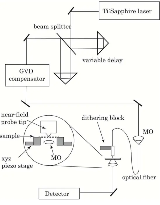
One of the typical optical fiber based ultra-fast SNOM setup is shown in Figure 1.1. An illumination-mode configuration is adopted here. Pulses from a femtosecond Ti:sapphire laser are split into two parts by a beam splitter, with an intensity ratio of 1:1. The two beams are combined again and then incident into a GVD compensator to pre-compensate the GVD arising from all the optical components involved. The laser pulse is then coupled to an optical fiber that has an aperture probe at another end.
The tip is mounted onto a mechanical block that includes adjustment screws to approach the probe tip close to the surface of the sample. After the tip is approached to the sample surface within the range of the Z-axis piezo-stage displacement, a shear force feedback method is turned on to control the gap between the tip and the sample surface to be a few nanometers. The probe is driven by a dithering piezo stage and oscillates at a resonant frequency, and moved closer to the surface, while the oscillation amplitude is detected by shining an infrared laser on the probe and measuring the reflected signal with a photodiode. The oscillation of the probe will be damped as it approaches to the surface and in this way the probe tip can be maintained within few nm from the sample surface by the feedback method. The shear force feedback is also used to obtain a topographic image analogous to that
obtained with an AFM.
Beneath the sample, an objective lens with a high NA value (>0.8) was set to collect the luminescence emitted from the sample. A photo-multiplier tube (PMT) or photon counting photodiode was used to detect the optical signal. The ultrafast SNOM system could be used to investigate various kinds of ultrafast dynamics in nanomaterials. In this thesis, we mainly focus on the research of surface plasmon
Fig. 1.1 Schematic setup of an ultrafast scanning near-field optical microscope. MO: micro objectives.
dynamics of gold nanoparticles.
1.3 Surface plasmon dynamics
When a metal nanostructure is shined by light, the conduction electrons within the penetration depth of the excitation from the metal surface translate collectively with respect to the lattice of the positive charges. The attractive forces between negative charges of the electrons and positive charges of lattice ions give a restoring force for the collective motion resulting in a collective oscillation of the electrons. The collective oscillation of the conduction electron that typically occurs at the surface of metal nanostructures is called surface plasmon resonance (SPR). The individual electrons move stochastically but a superstition of many independent electron oscillations yields collective oscillation of electrons. The collective oscillation of electrons damps via radiative and nonradiative damping (T1 process described later) and via randomization of the phase relations among individual electron oscillations by elastic collisions (T2* process). The resonance frequency of the oscillation is controlled by the microscopic restoring force, as well as by dielectric environment determined by the particle size, shape and the surrounding medium. Many works were devoted to studies on the characteristics of SPR as a function of particle size, shape and dielectric properties, while more detailed behavior of ultrafast dynamics of SPR for a single metallic particle have still remained to be revealed [39-42].
Excitation and relaxation of SPR in metallic nanoparticles play an important role in linear and nonlinear optical effects of them, such as the extinction spectral characteristics, local field enhancement, and so forth. The studies of dynamic behavior of SPR in the time-scale from a few femtoseconds to several picoseconds help us to get fundamental knowledge about the basic properties of the light-matter interaction in metallic nanoparticles. One of essential issue among them is how fast the collective excitation loses their phase coherence, and what is the internal
mechanism that controls this procedure.
Generally speaking, the energy relaxation of materials proceeds in several steps [43]. Initially, the electrons absorb the energy of photons via interband and/or intraband transitions. The resultant electron distribution is highly non-thermal and strongly correlated in the time scale of few femtoseconds. After the phase coherence of the excitation is lost, the first energy relaxation step is the electron thermalization by electron-electron scattering, which establishes a new Fermi electron distribution with a higher temperature than that before photoexcitation. The energy is transferred into quasi-particle pairs (electron hole pairs). The electron-electron scattering redistributes the excitation energy to thermalize the electron gas. Quasi-elastic electron-phonon and electron-surface scattering do not play a dominant role in this stage in the dissipation of the excess energy of laser excited hot electrons. Fan and co-workers have shown, through the time resolved photoemission experiment for a gold film, that the temporal scale of this thermalization process is of a few hundreds of femtoseconds [44].
Then the thermalization process to the lattice occurs as the next step. The energy is transferred from the hot electron system to the relatively cold lattice of the nanoparticles. This process has been studied in detail for thin films made of various noble metals. In general, it takes about a few ps until a quasi-equilibrium state is formed between the electron system and the lattice (phonon) system. This heat-exchange process is also described as the electron-phonon coupling process [45-49].
The last step in the energy relaxation is the heat transfer between the nanoparticles and the surrounding medium. The relaxation occurs in a time scale of several ps to hundreds of ps. This process is sensitive to the thermal conductivity of the surrounding medium. In this time region, the lattice temperature of the
nanoparticles is considered to be the same as the electron temperature [50-52].
The dephasing procedure of SPR, of which time constant is usually denoted as T2, takes place in the first step of relaxation immediately after the photoexcitation which consists of inelastic decay process (time constant T1) and the pure dephasing (time constant T2*). The first part is a decay due to the energy transfer from plasmon into formation of electron-hole pairs or reemission of photons (radiation damping), while the second is a randomization of the phase relations among the individual electron oscillations due to elastic collisions [53]. The relationship among them is given in Equation (1.2):
= Γ⋅ = ⋅ + ∗ 2 1 2
1 2
1 2
1
T T h
T (1.2)
where Γ is the homogeneous linewidth of the plasmon resonance.
Many experiments have been performed in order to determine dephasing times of metal nanopartilces. Lamprecht measured the dephasing time for lithographically prepared gold nanoparticles using a second-order nonlinear optical autocorrelation method in the femtosecond regime at far-field. The obtained dephasing time was found to be 7 fs for ~200 nm gold nanoparticles [54-55].
Since size and shape distribution of the nanoprticles affects the measurements of dephasing times in ensemble measurements, it is advantageous to perform the measurement on single nanoparitcles. Liau and his co-workers performed the second-order interferometric autocorrelation measurement on single silver nanoparticles by combining an optical microscope with an AFM. They got a dephasing time of 10 fs for 75 nm silver nanoparticles [56].
Another way to estimate dephasing times while overcoming the problem of inhomogeneous broadening due to variations of size and shape is to adopt the
single-particle spectral width measurements. Klar et al. performed the near-field transmission spectral measurement on gold nanoparticles with averaged size of 40 nm. They extracted the dephasing time from the homogeneous linewidth, which was around 8 fs [57]. Soennichsen et al. investigated the dephasing time of single gold nanorods based on single-particle light-scattering spectroscopy, and observed the dephasing time ranging from a few fs to 20 fs depending on the aspect ratio of the nanorods [58]. Spectral hole burning is another technique used to investigate the dephasing time in metallic nanoparticles. By subtracting the absorption spectrum of nanoparticles before and after the laser irradiation, the decay time was found to be 4.8 fs for silver nanoparticles with the radius of 7.5 nm [59].
As mentioned above, experimental investigations on dephasing of noble metal nanoparticles have been performed via time-domain measurements of ensembles of particles or frequency-domain light scattering spectral measurements of ensembles or single particles [54-59]. With ultrafast SNOM method, we can study the single-particle plasmon dynamics in the time domain (possibly even position dependence measurements in a single particle) with very high time and spatial resolution.
1.4 Ultrafast Measurement Technique
1.4.1 Principle of pulse duration measurement
In this section, the principle of pulse duration measurement (and that of dephasing measurements in the following subsection) is briefly explained. In the ultrafast SNOM system, the time resolution is determined by the pulse duration at the probe tip. Although principle of the measurements is explained for the far-field
measurement, the basic idea is applicable to the near-field measurement as described in Section 3.
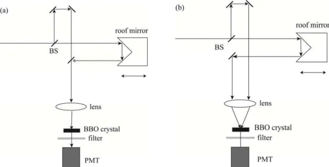
The characterization of the temporal profile of the laser pulse is the basis of any ultrashort laser optimization and the prerequisite of any ultrafast measurements. However, response times of photoelectric devices are generally limited to nano to picosecond regime and therefore the optical methods based on autocorrelation techniques should be adopted. There are several conventional methods of autocorrelation measurements, such as intensity autocorrelation, and fringe-resolved autocorrelation. In this work, we mainly utilized the fringe-resolved autocorrelation method to determine the pulse duration [60].
In the autocorrelation methods, the laser beam is split into two identical beams by a beam splitter as shown in Fig. 1.2. One of the two pulses is delayed from the other for a variable time delay τ. The beams of the two arms are collinearly recombined (in the case of collinear configuration) and are then focused onto a thin nonlinear crystal,
Fig. 1.2 Basic experimental setup of second-order autocorrelation measurement. (a) Collinear configuration and (b) non-collinear configuration. BS: beam splitter, PMT: photo multiplier tube.
such as a BBO crystal. The autocorrelation trace is then recorded by plotting the second harmonic intensity as a function of τ.
The expression for the second-harmonic intensity under the collinear configuration is given as
I
[
E t E t]
dt E t E t E t E t dt2 2 2
2
2 ( ) 2 ( ) ( ) ( )
) ( ) ( )
(
∫ ∫
+∞
∞
− +∞
∞
−
− +
− +
=
− +
= τ τ τ
τ (1.3)
where E(t) and E(t–τ) are the electric fields for the two arms of the interferometer, respectively, and τ is the time delay between two arms.
We can then obtain the intensities of the signal in the cases τ = 0 and τ = ∞ as, for a Fourier-transform-limited optical pulse.
I(τ =0)=24
∫
E4(t)dt (1.4) I(τ =∞)=2∫
E4(t)dt (1.5)The ratio between the intensities at τ = 0 and τ = ∞ should be 8:1 in this case. If the pulse is chirped, regardless whether with linear or nonlinear chirp, this ratio is decreased. This can be used as a criterion to judge whether the pulse is chirped or not.
There is a relationship between the full width at half maximum (FWHM) Δt of the autocorrelation trace and the real pulse duration Δτ depending on the pulse shape. In order to know the real pulse duration, we first have to assume a realistic pulse shape. Table1.1 summarized the relation between Δt and Δτ for some typical pulse shapes. The sech2 pulse shape is commonly adopted as a realistic one for mode-locked laser outputs. This assumption for the pulse shape will be also adopted
in this thesis. In this case Δτ / Δt is set to be 1.54.
1.4.2 Principle of SPR dephasing time measurement
As discussed in Section 1.2, there are various ways to estimate the dephasing time of SPR in the metal nanoparricles, either directly in the time-domain or indirectly in the frequency-domain. In the present work, we adopted time-correlated two-photon-induced photoluminescence (TPI-PL) method, which enables a pump-probe technique to directly measure the dephasing time in the time domain [61-63].
The principle of time-correlated TPI-PL is schematically shown in Fig 1.3. A pump pulse E(t) is incident on the metal nanoparticle (the pulse is assumed to be centered at t = 0), which excites the nanoparticle to a plasmon resonance state. Subsequently, a probe pulse E(t–τ) photoexcites the particle after a delay time of τ to a higher level, which emits photoluminescence in the wavelength region shorter than the incident light. The emitted photoluminescence yield is determined by the transient
I(t) Δt Δτ Δτ / Δt
t2
e− 1.665 2.355 1.414
sech2(t) 1.763 2.72 1.543
) /( ) /(
1
A t t A t
t e
e − + − − A=1/4
1.715 2.648 1.544
A=1/2 1.565 2.424 1.549
A=3/4 1.278 2.007 1.570
Table 1.1 Relationships between autocorrelation FWHM Δτ and pulse intensity FWHM Δt.
population of the plasmon-resonant intermediate state and the relative phase of the
probe field with respect to the plasmon oscillation, which depend on the pump-probe time delay. The measured time-correlated TPI-PL signal contains the information on the dephasing of SPR, which is reflected on the width of the TPI-PL correlation profile. The incident laser field induces a plasmonic field on the surface of a gold nanoparticle, which is a convolution of the laser filed and response function of the surface plasmon. This response function of the surface plasmon decays with a dephasing time τ. Consequently, the plasmonic field lasts longer than the laser field, as illustrated in Fig 1.4 based on the formula given below. Since the TPI-PL process is governed by the plasmonic field, the TPI-PL correlation profile is broadened due to the finite dephasing time.
Lamprecht et.al proposed a model to analyze the influence of plasmon dephasing on the FWHM of the time-correlated TPI-PL profile [64, 65]. In this model the
τ) of a single particle for a given pulse delay time τ
Fig 1.3 Mechanism of the time-correlated TPI-PL. PL indicates the photoluminescence.
EPl(t;τ) ≈ 1 ω0
−∞
∫
t K (t∗,τ)e−γ(t−t∗)sin[
ω0(t− t∗)]
dt∗ (1.6)with
K (t∗,τ) = E(t∗)+ E(t∗− τ), ω0=2πc λres
, γ = 1 2πτdp
where λres denotes to the resonance wavelength, c the speed of light, and τdp is the dephasing time of SPR. We can then calculate the time-resolved correlation signal profiles based on Equation (1.6) for given dephasing times τdp. By comparing the measured TPI-PL autocorrelation profile with the simulated curve, the depahsing time of SPR can be estimated.
60 40 20 0 -20 -40
100 50
0 -50
Time (fs)
plasmon field
laser field
Intens ity (a.u.)
Fig1.4 Temporal behavior of pulse laser field (red) and the resonantly driven plasmon field (black).
Chapter 2
GVD arising from optical components and devices
generating negative GVD
2.1 Introduction
Since various dispersive media are used as optical components in SNOM, the time resolution of ultrafast measurements in SNOM is usually deteriorated due to GVD arising from the optical fiber as well as other optical elements. Ultrashort pulses are seriously broadened by the GVD effects. Fig. 2.1 shows a typical example of pulse broadening where an autocorrelation trace is plotted for 15-fs laser pulses after passing through a 150 mm length optical fiber. The FWHM of the autocorrelation trace is around 6 ps, which means that the pulse duration was elongated for several orders after passing through the optical fiber. Such a broadened pulse cannot be used for the ultrafast measurements in the SNOM.
䢶䢲䢲
䢵䢲䢲
䢴䢲䢲
䢳䢲䢲
䢲
Time delay (2 ps/div.)
Inten sity (a.u.)
Fig. 2.1 Autocorrelation trace of a 15-fs pulses propagated through a 150 mm optical fiber.
In order to obtain very short pulse duration at the probe tip of the SNOM, this huge GVD must be removed by some means. There are several methods to remove the GVD, including the passive devices such as prism pair [66] and grating pair [67], and active pulse shaping techniques, for instance, by using liquid-crystal modulators [68], acousto-optic modulators [69] and deformable mirror (DFM) [70]. Each of them has their own unique characteristics, and can be used for different purposes. The characteristics of prism pair, grating pair, and DFM will be discussed in the following subsections. In this thesis, the combination of these three devices was finally adopted for the ultrafast SNOM.
Before performing any actual experiments, we estimate how much positive GVD optical fibers generate, and how much negative GVD the above-mentioned devices can introduce.
2.2 Estimation of GVD arising from the optical fiber
For a single-mode optical fiber used in the near-field probe, the material dispersion is the dominant reason for pulse broadening, which is caused by the wavelength dependence of the refractive index of the material. The intensity dependence of the refractive index also leads to nonlinear effects due to the self-phase modulation [71, 72] if the peak intensity of the incident laser is high, but such nonlinear effects are not serious in the present case and not considered in this thesis. The refractive index of doped silica (the material used for single-mode optical fibers) can be approximately described by the empirical Sellmeier equation [73]:
∑
= −
− 3 2
2
2( ) 1 j
B n A
λ λ
λ (2.1)
where n is the refractive index, λ is the wavelength in unit μm,Aj and Bj are experimentally determined Sellmeier coefficients. Note that this λ is the vacuum wavelength, not that in the material itself.
Since we have no detailed information on materials of the optical fiber for the near-field probe, we assume here that the optical fiber is made of fused silica doped with GeO2. The corresponding values of the coefficients Aj and Bj for doped fused silica are summarized for a few of dopant concentration in Table 2.1 [74, 75].
By using the Eq. (2.1) with the coefficient in Table 2.1, the value of n(λ) at a specific wavelength for an optical fiber can be estimated. The values of dn/dλ and d2n/dλ2 can also be obtained consecutively. The dispersion parameters are shown in Table 2.2 [76]. We can then calculate the second-order GVD for the optical fiber according to the equation [77],
Dopant (%) A1 A2 A3 B1 B2 B3
GeO2 (0%) 0.696 0.408 0.897 0.00468 0.0135 97.9
GeO2 (6.3%) 0.708 0.420 0.866 0.00792 0.0105 97.9
GeO2 (19.3%) 0.735 0.446 0.808 0.00585 0.0155 97.9
Table 2.1 Coefficients of Sellmier equation for GeO2-doped fused silica
Dopant n(λ) dn/dλ /104 m-1
d2n/dλ2 /1011 m-2
d3n/dλ3 /1018 m-3
d2ψ/dω2 /104 fs2
d3ψ/dω3 /104 fs3 GeO2 (0%) 1.4533 -1.7 0.4 -0.2 0.5435 0.1062
GeO2 (6.3%) 1.488 -1.788 0.459 -0.23 0.6691 0.2666
GeO2 (19.3%) 1.5248 -1.968 0.582 -0.291 0.7655 0.3352
Table 2.2 Dispersion parameters of silica doped with GeO2 at λ = 800 nm and GVD for optical fibers (150 mm) made of respective materials.
2
2
2 3
2 2
d d 2
d d
λ πλ
ωψ
L n c
= c (2.2)
L d
n d d
n d c
c c c
c ⎟⎠⎞ ⎜⎜⎝⎛ + ⎟⎟⎠⎞
⎜⎝
−⎛
= 3
3 3 2 2 2 2
3 3
1 3 2 d
d
λ λ λ λ
λπ
ωψ (2.3) where λc is the central wavelength of the laser pulse, ψ is the phase delay, ω is the angular frequency, and L the length of the optical fiber.
In our case, λc = 800 nm and L =150 mm. We can then get the amount of GVD arising from the optical fiber. As is seen in the estimated values in Table 2.2, the positive GVD arising from the optical fiber is large, even for the pure silica. In the case of GeO2 doped silica, the GVD increases with the dopant concentration.
We have considered here the material dispersion arising only from the optical fiber. Actually, there are many other optical elements used in the SNOM system, such as lenses, beam-splitters and mirrors. All of them also yield GVD. These GVD contributions further broaden the pulses and hence degrade the time resolution of the ultrafast SNOM measurements.
2.3 Estimation of GVD generated by a prism pair
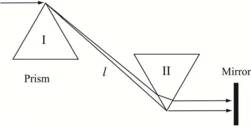
Prism pair has been widely used for dispersion compensation since they have the advantage of very low energy loss. Since the refractive index varies with wavelength, the laser beam is dispersed after transmission through the first prism (Fig. 2.2). The short wavelength component is refracted more strongly than the long wavelength component. Therefore, the short wavelength component propagates longer distance through the space between the two prisms than the long wavelength component, while the long wavelength component travels through the prism medium for a longer
distance. This effect introduces a wavelength dependent phase shift, which varies with the distance between the prisms (l in Fig. 2.2) and the position of the second prism. We can use a mirror to reflect the beam back so that it passes through the same prisms. This is a folded geometry of the prism sequence compressor [77].
A typical schematic setup of folded geometry of the prism compressor is shown in Figure 2.2. The first prism disperses the beam, while the second prism collimates the dispersed beam.
The GVD introduced by the prism pair is given by,
d2ψ dω2 = λ
c 3
2πc2 Ln ′ ′ − 4l⋅ ( ′ n )
[
2]
(2.4)( )
2 2[
12(
2[
1 ( 3 2 )] )
(3 )]
4
3 3
n n L n n n
n n n
c l d c
d
c c
c
c ′ − ′ − + ′ ′′ − ′′+ ′′′
= λ − λ λ
πλ
ωψ (2.5)
where n is the refractive index of the prism material, n'(λ) = dn/dλ and n"(λ) = d2n/dλ2, λc is the central wavelength of light, l is the separation between the prisms, and L is the path-length through the prisms [77].
The first term of Eq. (2.4) is always positive and depends on the path-length through the prisms. The second term is always negative and the value mainly
Fig. 2.2 Schematic setup of a prism pair.
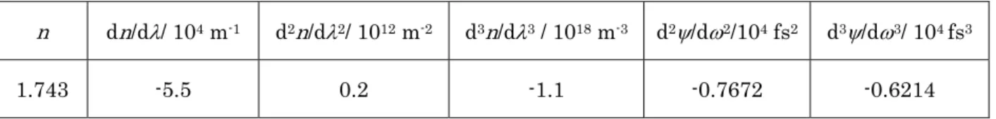
depends on the prism separation. By varying the prism separation and the path length through the prisms, we can control the sign and the amount of introduced dispersion. Therefore, in principle, any amount of negative GVD can be generated if large enough prism pair is provided. In practice, however, the size of the prism pair is limited. In the present study, we used two prisms made of SF14 glass and one mirror to make a folded prism compressor, with each prism of 50-mm side length. Since the laser beam width after dispersed by the first prim must be smaller than the side length of the second prism, the separation between the two prisms l is limited to be less than about 700 mm. The dispersion parameters of SF14 glass and the maximum (negative) values of second- and third-order GVD thus calculated with Eqs. (2.4) and (2.5) are summarized in Table 2.3. Since we adopt folded geometry of the prism sequence, the amount of second- and third-order GVD should be doubled. Comparing with the positive GVD arising from optical fiber (see Table 2.2), it suggests that the prism pair can be used to compensate the GVD if the device is large enough.
2.4 Estimation of GVD generated by a grating pair
A parallel grating pair could give much larger angular dispersion comparing with that of prism pair. Similar to the prism compressor, it also generates angular
n dn/dλ/ 104 m-1 d2n/dλ2/ 1012 m-2 d3n/dλ3 / 1018 m-3 d2ψ/dω2/104 fs2 d3ψ/dω3/ 104 fs3
1.743 -5.5 0.2 -1.1 -0.7672 -0.6214
Table 2.3 Dispersion parameters of SF14 glass and second- and third-order GVD generated by a SF14 prism pair with the separation between the prisms l = 700 mm, at λc = 800 nm.
groove number / mm–1 d2ψ/dω2 / 104 fs2 d3ψ/dω3 / 104 fs3
300 -0.429 0.6
600 -1.62 2.66
800 -2.98 5.73
Table 2.4 Second- and third-order GVD generated by grating pairs with different groove numbers/
dispersion. The beam of ultrashort laser pulse is incident on the first grating at the blazing angle. The dispersed beam is then incident on the second grating that is
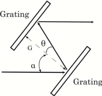
identical to the first one. The two gratings are arranged fully parallel to each other. Each spectral component of the dispersed beam travels its inherent distance. The higher frequency components arrive earlier than the lower frequency components, resulting in a negative GVD of the grating pair or frequency-dependent phase shift. This concept was first demonstrated by Treacy [67]. He proposed a grating pair as a device that generates negative dispersion as shown in Fig. 2.3.
The equations for calculation of second-order and third-order GVD are given in
Fig. 2.3 Grating pair that generates negative dispersion.
Equations (2.6) and (2.7) [77].
d2ψ dω2 = − λ
c
2πc2( λ
c
d )
2 G
cos3θ (2.6) d3ψ
dω3 = − 3λc 2πcos2θ cos
2θ+ λc
d ( λ
c
d +sinα)
⎡
⎣ ⎢
⎤
⎦ ⎥ d2ψ
dω2 (2.7)
where G is the separation between grating surface planes, d is the grating constant (separation between the grooves), λc is the central wavelength of the input laser pulse, α is the angle of incidence on the first grating, and θ is the angle between dispersed beam and normal vector of the grating.
If the laser pulse is normally incident on to the first grating and G = 50 mm, we obtain the amount of second- and third-order GVD as summarized in Table 2.4. Comparing with the values in Table 2.2, where the GVD were calculated for an optical fiber, a grating pair may provide negative GVD that is suitable compensate for the positive GVD generated by the fiber if the groove number of the grating is 300 mm–1. If the groove number is 600 or 800, it will give excess negative GVD to compensate for the positive GVD generated by the fiber. From Equation (2.6), the larger separation between two gratings and/or the larger groove numbers of the gratings, the larger negative GVD the grating pair generates.
It is also worth noticed when we compare the GVD for a prism pair and a grating pair (Tables 2.3 and 2.4), that the third-order GVD for a grating pair has an opposite sign to that for a prism pair. This means that, by suitably choosing the device parameters, both second- and third-order GVD generated by an optical fiber can be removed to a certain degree if we combine a grating pair and a prism pair.
To summarize, we can roughly estimate GVD arising from the optical components involved in the system based on the formulae given above. It is important to get rough estimation of suitable device parameters to design the optimized
measurement system.
2.5 Deformable mirror setup
2.5.1 Principle of the deformable mirror
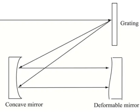
Although prism pair and grating pair have great ability to compensate GVD, a severe problem for these methods is the interdependence of different phase orders, which prevents perfect compensation for arbitrary phase. For example, a grating pair gives negative second-order GVD, meanwhile, it also generates non-negligible positive third-order GVD. This means if we use only a prism pair or a grating pair in the GVD compensation setup, it is hardly possible to remove the entire chirp, and hence it cannot fully recover the pulse duration. The active pulse compression techniques by the use of phase modulation devices such as liquid-crystal modulators (LCM), acoustic-optic modulators (AOM), or deformable mirror (DFM) have a potential to overcome this problem. They have the ability to finely remove the higher-order GVD and have already been widely used in various ultrafast measurements. As for the AOM and LCM, they required an unfolded 4f configuration since they are transmissive devices. Additionally, LCM could not provide continuous phase modulation due to the pixilated system, while AOM requires very careful synchronization of the radio-frequency waveform to the laser pulse. In this thesis, the DFM is adopted for the purpose of fine phase adjustments for pulse compression. One of the advantages of the DFM is its smoothly varying phase modulation, in addition to low energy losses (98% reflection). A basic schematic pulse compression setup of a 4f system with a DFM is shown in Figure 2.4, where a grating is used to disperse the wave components of laser pulse, and a concave mirror is used to collimate the dispersed beam incident on the DFM
perpendicularly. The grating, concave mirror, and DFM hence make a folded 4f system.
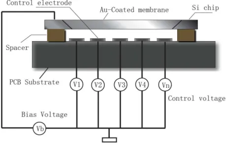
The schematic drawing of the assembled DFM and the principle of biased control are illustrated in the Fig. 2.5. The voltage applied to the actuator makes a force to push or pull the mirror, and deforms the surface shape. The surface shape is determined by the combination of all the influence from the actuators. The phase change that the deformable mirror can generate is given in the following equation [72]
φ =2
( )
2π Δz/λc (2.8)where Δz is the mirror displacement normal to the surface, λc is the central wavelength of the pulse. As an ideal case, we assume that the mirror bend radius is negligible. Since the DFM we adopted is capable to give 9-μm maximum
Fig 2.4 Schematic setup of a 4f system with a deformable mirror.
displacement in the center position, the maximum phase change would be 45π.
2.5.2 Genetic algorithm to control the DFM
In order to use the DFM for the pulse compression purpose we have to get a signal that reflects the pulse duration and feed-back control the DFM surface to yield the optimum signal level. For this purpose, second harmonic generation (SHG) signal of the laser pulses is utilized to be optimized. The SHG signal becomes highest when the pulse width is the shortest. Thus the pulse width is optimized by maximizing the SHG signal. To maximize the SHG signal, genetic algorithm (GA) is useful. So a control software for the DFM based upon GA was developed. The GA is a highly efficient and robust search algorithm that simulates evolution in nature [78, 79]. The schematic procedure of the GA in the present study is shown in Figure 2.6.
The basic principle of GA was originally proposed by Holland [78]. It is inspired by the mechanism of evolution by natural selection, where a stronger individual has a greater chance to survive in a competitive environment. In the GA, the candidates of solutions to a problem are regarded as 'individuals' and are parameterized as 'chromosomes'. In each cycle of the evolutionary procedure, a fitter chromosome
Fig 2.5 Schematic drawing of a deformable mirror. PCB: polychlorinated biphenyl
generates 'offspring' through crossover and mutation. The 'offspring' with better quality is selected and takes the place of their 'parents' through fitness evaluation, which means a better solution to the problem is generated.
In our case, the simplest GA schematically shown in Fig. 2.6 is interpreted as follows.
1. Initialization of the gene population
Start with a randomly generated population of N 'chromosomes', which are
Fig. 2.6 Schematic flow of the genetic algorithm adopted.
candidate arrays of voltages (Vk;k=1…N)applied to the element actuators of the DFM. The notes ai[0] to ai[m] below denote the voltages applied to the actuators. V1 a1[0], a1[1], a1[2],……… a1[m]
V2 a2[0], a2[1], a2[2],……… a2[m] ……
…… ……
VN aN[0], aN[1], aN[2],………… aN[m] 2. Fitness evaluation
For each chromosome (array of the voltage set Vk applied to the DFM) the SHG signal fk of the pulses after propagating through the system is collected by the PMT. This signal serves as the fitness parameter for the chromosome Vk. We obtain N fitness parameters (f1, f2, ... ,fN) for (V1, V2, ... , VN )when this step is finished.
3. Selection
In the present case, a roulette wheel approach is adopted as the selection procedure of the chromosomes. These voltage arrays Vk yielding higher SHG intensity have more chances to be selected, while the other ones is abandoned. The roulette wheel procedure is progressed as described below:
z Step1: Sum up the SHG intensity of all voltage arrays, F = Σ fk
z Step2: Calculate selection probability pk for each voltage array Vk as pk = fk/F
z Step3: Calculate cumulative probability qk = p1+p2+ ... +pk for each voltage array Vk
z Step4: Generate a random number r within the range of [0,1]
z Step5: If r ≤ q1, then select the first array V1; otherwise, select the k-th
array Vk(k = 2,3, ..., N) such that qk-1< r ≤ qk
4. Crossover
This operator exchanges some voltage values of two voltage arrays (i.e., chromosomes) to create two chromosomes of offspring, with a probability varying from 0 and 1. For example, the voltage arrays of the first two chromosomes:
V1 a1[0], a1[1], a1[2],……… a1[m] and V2 a2[0], a2[1], a2[2],……… a2[m]
are crossed over by exchanging the first two voltages, and in this case the new chromosomes of offspring are:
V1 a2[0], a2[1], a1[2],……… a1[m] and V2 a1[0], a1[1], a2[2],……… a2[m]
This operator roughly mimics biological recombination between two single-chromosome organisms. If no crossover takes place, it generates two individuals that are the exact copies of their respective parents.
5. Mutation
This operator changes some voltage(s) in a voltage array (chromosome) with a probability ranging from 0 to 1. For example, the value of a1[2] in V1 is changed with a randomly chosen value in the mutation:
V1 a1[0], a1[1], a1'[2],……… a1[m]
6. End condition.
If the highest SHG signal is obtained, which means the best solution (fittest to the problem) is found, or it reaches the pre-set maximum iterative number, then the process of the algorithm terminates.
Chapter 3
Basic performance of pulse compression devices
combined with fiber-probe SNOM
published in part in
H. J. Wu, Y. Nishiyama, T. Narushima, K. Imura, and H. Okamoto, Applied Physics Express 5 (2012) 062002.
In this chapter we examine the basic performance of the pulse compression system, for a few of combinations of GVD compensation devices (prism pair, grating pair, and 4f optical system with DFM). The width of ultrashort optical pulses are measured after propagating the pulse compression system and the optical fiber, based mainly upon interferometric (fringe-resolved) autocorrelation measurements.
3.1 Combination of prism pair and DFM
In Chapter 2 we tried to calculate GVD for the optical fiber and the GVD compensation devices. The results show that the combination of prism pair and deformable mirror might give enough negative GVD to compensate the positive GVD arising from the optical components. Therefore, we first launched the experiment to check the performance of this GVD compensator with the setup shown in Fig. 3.1. This is a far-field measurement of the pulse duration (the near-field microscope is not installed), since it is advantageous for checking performance due to easier alignment and much simpler experimental configuration comparing with the near-field measurement. It still provides useful information on the performance of the compensator, however.
In this setup, the laser pulse centered at 800 nm (~15 fs pulse duration) was incident on a reflection type grating (600 grooves/mm), and the dispersed light was collimated by a concave mirror to incident on the DFM. These optical elements form a 4f system. The DFM was a product of OKO Technologies, based on the technology of silicon bulk micromachining. The device consists of a silicon membrane mounted over a printed circuit board holder. The membrane (11 mm x 39 mm) is coated by a gold film and suspended over an array of 19 actuator electrodes on a printed circuit board. The 19 actuators are arranged linearly below the membrane. The maximum
displacement of the mirror surface in the center position of the mirror is 9 μm. The reflected-back beam was then picked out and sent to the SF14 prism pair. The apex angle of each prism is equal to the Brewster angle at a wavelength of 800 nm. The prisms were arranged in such a way that the beam entered in and exited from each prism at the Brewster angle. The laser beam was then coupled into a 150-mm long optical fiber. At the other end of the fiber, another objective lens was used to collimate the optical output from the fiber. The beam was separated into two parts after the fiber and the lens. One was incident on an autocorrelator for the far-field autocorrelation measurement, and the other was focused onto a 100-μm BBO crystal to generate the feed-back signal for the DFM control. The generated SHG radiation was detected by a PMT and the signal was sent to the computer as the parameter for the GA. The distance between the two prisms was set to be ~700 mm in order to get as large as possible negative GVD, which was the maximum separation in the
Fig 3.1 Schematic experimental setup for the far-field autocorrelation measurement with a prism pair.
Fig 3.2a shows the autocorrelation trace measured before the optimization process of the DFM at a position after the optical fiber. The FWHM of the trace is ~83 fs, which corresponds to the pulse duration of about 55 fs. The peak-to-background ratio is about 7. Fig 3.2b shows the autocorrelation trace after the optimization of the DFM to maximize the SHG intensity. The optimization procedure was finished (i.e., the SHG intensity reached its maximum) within 200 generations in ~5 minutes, as shown in Fig 3.2d. The FWHM of the autocorrelation trace is reduced to about 67 fs, which corresponds to the pulse duration of about 44 fs. However, the
䢸 䢷 䢶 䢵 䢴 䢳
Time delay (20 fs/div.)
Intensity (a.u.)
(a) 䢹
䢸 䢷 䢶 䢵 䢴 䢳 䢲
Time delay (20 fs/div.)
Intensity (a.u.)
(b)
200
150
100
50
0
15 10
5 0
Acutator number
Voltage (V)
(c)
1.8
1.6
1.4
1.2
500 400 300 200 100 0
Intensity (a.u.)
Generation
(d)
Fig.3.2 (a) Autocorrelation trace before optimiazation of DFM. (b) Autocorrelation trace after optimiazation of DFM. (c) The voltage applied to each actuator of the DFM after
optimization. (d) The intensity of the SHG signal as a function of the generation.
peak-to-background ratio is still about 7. The pulse duration after optimization of the DFM did not change much, and was still far from the original pulse duration of the laser output (~15 fs). It indicates that serious GVD remained.
The separation between two prisms is a key parameter that determines the amount of negative GVD. As we discussed in Chapter 2.3, the prism material itself also generates positive GVD. If the separation is not enough, it does not have an ability to compensate the positive GVD due to the fiber. It may even add additional positive GVD to the laser pulse. The maximum second-order negative GVD that could be generated by the SF14 prism pair is -15344 fs2, while the positive GVD generated by a 150 mm optical fiber (19.3% GeO2 doped) is 7655.05 fs2, as shown in the calculation of the previous Chapter. From this estimation, we may expect that the positive GVD due to the optical fiber may be compensated by the negative GVD introduced by the prism pair. The reality is, however, the original pulse width was not recovered at the position after the fiber even after the optimization of the DFM. The situation was not improved even when the prism distance was shortened. The origin of this unfavorable result has not been clear yet, but there may be a few of possible reasons. It may partially be due to other optical components in the system such as lenses and mirrors and difficulties in precise alignments of the setup. It may be also conceivable that the GVD of the fiber is actually larger than that estimated. The negative second-order GVD produced by the prism pair is possibly not as high as calculated because, for example, the beam practically have to travel through the glass longer than the ideal case due to the finite beam size. As for higher-order GVD, although the signs of second- and third-order GVD by the prism pair device estimated in Chapter 2 (-15344 fs2 and -13428 fs3, respectively) are both opposite to the corresponding ones generated by the fiber (7655 fs2 and 3352 fs3 for 19.3% GeO2), the respective magnitudes do not match quantitatively. This fact may also affect the
performance of the GVD compensation system.
Fig. 3.2c shows the voltage applied to each actuator of the DFM after the optimization process. The horizontal axis corresponds to the lateral position on the DFM surface. Since the voltages applied to the actuators determine the displacements normal to the surface of the mirror, they may give us a qualitative measure of the surface shape of the DFM. From the surface shape, we can judge roughly whether the GVD has been removed. If the voltage curve is smooth enough (= surface shape is smooth) and the applied voltages are within a relatively small range, it shows that the GVD has been in most part removed. If the curve is not smooth and/or the voltage amplitude is close to the maximum applicable voltage of the DFM (~250 V), it means the GVD is too much to compensate for with the GVD compensator. In Fig. 3.2c it is clear that the voltage applied to some of actuators were saturated. This observation shows that the prism pair and the DFM are not sufficient to remove all the GVD generated from the optical fiber and other optical elements.
3.2 Combination of grating pair and DFM
The combination of prism pair and the DFM could not provide enough negative GVD for the full compensation of GVD due to the fiber and other optics. We thus tried another type of GVD compensator, which consists of a grating pair and the DFM. The experimental setup for the measurement is shown in Fig. 3.3. In this setup the autocorrelation measurement was performed in the near-field regime. The output from the laser source with a pulse width of ~15 fs was split into two parts, with the intensity ratio of 1:1. In one arm of the optical-delay setup a piezo-stage