Built-in Self-Test for Functional Register-Transfer Level using
Assignment Decision Diagram
Norlina Binti Paraman1, Chia Yee Ooi1, Ahmad Zuri Bin Sha’ameri1 and Hideo Fujiwara2
1Faculty of Electrical Engineering University Teknologi Malaysia
81300 Skudai Johor, Malaysia {norlina, ooichiayee, zuri}@fke.utm.my
Abstract - Built-in Self-Test (BIST) currently has high area overhead and long test application time. In this paper, we propose a new BIST technique at functional register-transfer-level (RTL) which is based on the test-per-clock scheme. We modify the original register into multiple input signature register (MISR) at behavioural descriptions to reduce area overhead. We test all combinational blocks simultaneously. This method results in lower area overhead, shorter test application time and comparably high fault coverage compared to the previous method.
Keywords : Built-in Self-Test (BIST); multiple input signature register (MISR); reduced BIST-able Register Transfer-Level (RTL) circuit
1.Introduction
With the advance in semiconductor technology, the complexity of Very-Large-Scale Integration (VLSI) designs is growing and the cost of testing is increasing. The external test with time consuming scan-in and scan-out of test data and expensive test equipment becomes more inefficient. The problems of the external automated test equipment (ATE) can be overcome by integration of built-in-self-test (BIST) technique in a circuit. In this technique [1], test pattern generators (TPGs) were added to primary inputs (PIs) and response analysers (RAs) were added to primary outputs (POs). Thus, the circuit is enabled to generate test patterns internally and compact the output responses. However, adding these TPGs and RAs are not sufficient to achieve high fault coverage (for single stuck-at faults), if the circuit contains feedbacks in its structure. Therefore, several techniques of design-for-testability (DFT) have been proposed [1].
Generally, BIST techniques are classified into test-per-scan scheme and test-per-clock scheme. In the test-per-scan scheme, the test registers generate test patterns and compact test responses in a few clock cycles based on scan-in and scan-out processes through scan path. The disadvantages of this scheme
2Faculty of Informatics Osaka Gakuin University Osaka 564-8511 JAPAN
are long test application time and cannot operate at- speed.
In the test-per-clock scheme, the test registers generate test patterns and compact test responses in one clock cycle. The advantages of this scheme are that at-speed is possible and test application time is short. However, test-per-clock requires higher hardware overhead than the test-per-scan scheme does.
BIST technique in the test-per-clock scheme [2,3,4,5] can be classified into two categories. The first category requires the simultaneous testing of all combinational blocks whereas the second category requires each module to be tested independently from the other modules. These two methods add test pattern generator (TPG) at all primary inputs and register analysers (RA) at all primary outputs. According to [2], they test all combinational blocks simultaneously. Their DFT method augments a given circuit with BILBO (built in logic block observer) or CBILBO (concurrent BILBO) so that the circuit becomes easily testable. Every feedback of the circuit must contain one CBILBO or two BILBOs. The advantage of this scheme is short test application time, since all combinational blocks are tested simultaneously. However, this scheme has high area overhead since several internal registers are modified to become BILBOs and CBILBOs.
In order to reduce hardware overhead in [2], Masuzawa et. al [3] proposed a BIST method based on hierarchical test where each combinational module is tested independently from other modules. The DFT method for this approach called single control testability. This scheme does not require to add extra register but only adds extra combinational logics to augment a given data path so that it is easily testable. In other words, the area overhead is lower than approach in [2]. The disadvantage of this scheme is long test application time because only a single combinational module is tested at a time. Yamaguchi et. al [4] proposed a new testability called concurrent single control testability to remedy the disadvantage of test application time approach in [3]. They extend the concept of the testability in [3] 12th IEEE Workshop on RTL and High Level Testing (WRTLT'11), pp. 9-15, November 2011.
by introducing concurrent testing so that multiple combinational modules can be tested concurrently at a time. This scheme has shorter test application time than approach in [3] but suffer from area overhead. In this paper, we propose a BIST technique of test-per-clock scheme and test all combinational blocks simultaneously. We classify the circuit into three categories based on BIST type and BIST insertion method to make the circuit BIST-able. They are called primitive BIST-able RTL circuit, concurrent BIST-able RTL circuit and reduced BIST- able RTL circuit. There is no element DFT augmented into primitive BIST-able RTL circuit. For concurrent BIST-able RTL circuit, the DFT augmented are following the Wunderlich [2] approach. In Wunderlich [2], they obtained short test application time and high area overhead. However, for reduced BIST-able RTL circuit we introduce DFT method. We improve approach in [2] by keeping the advantage of short test application time and resolving the disadvantages of area overhead. In order to reduce area overhead, we replace CBILBO in [2] with MISR for each feedback because MISR also can generate test pattern and compact test response simultaneously similar likes CBILBO. We also get similarly high fault coverage to that of the approach in [2].
This paper is organized as follows. In Section 2, we present the classification of BIST-able circuit where all combinational blocks are tested simultaneously. In Section 3, we define the DFT method for reduced BIST-able RTL circuit. In Section 4, we present the case study and Section 5 for conclusions.
2. Classification of BIST-able circuits
In this section, we classify the circuits into three categories based on BIST type and BIST insertion method to make the circuit BIST-able. They are called primitive BIST-able RTL circuit, concurrent BIST-able RTL circuit and reduced BIST-able RTL circuit. For primitive BIST-able RTL circuit, the original circuit is not augmented with DFT. For concurrent BIST-able circuit RTL circuit, the original circuit is augmented with DFT by inserting one CBILBO for each loop. For reduced BIST-able RTL circuit, the original circuit is augmented with our proposed DFT by inserting only a MISR for each loop. MISR can operate similarly to CBILBO to generate test pattern and compact test response simultaneously. To facilitate our discussion, we define the primitive BIST-able, concurrent BIST-able and reduced BIST-able as follows.
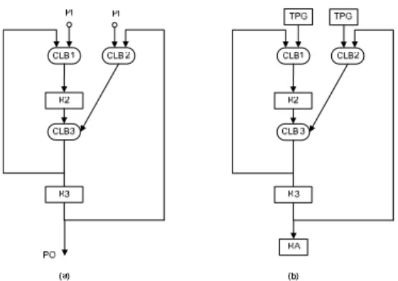
Definition 1. An RTL circuit is called primitive BIST-able if its primary inputs and primary outputs are modified into TPGs and RAs respectively.
Fig. 1. (a) Original RTL circuit with two connected self loops S1. (b) Primitive BIST-able RTL circuit. Example 1: Fig. 1(a) shows the original circuit which is not self-testable. Fig. 1(b) shows the primitive BIST-able RTL circuit. In order to make the circuit self-testable, we modify the PIs and POs into TPGs and RAs respectively as shown in Fig. 1(b). During testing, the TPGs apply pseudorandom patterns to CLB modules and the test responses of CLB modules are compressed by the register of PO which is modified into RA. Note that, the register R2 and R3 are not modified.
Referring to this example, there is no element DFT inserted into the primitive BIST-able RTL circuit. This approach obtains low fault coverage due to the feedback in the circuit. Note that for every loop, the register is not modified into test register. According to Wunderlich et. al approach in [2], they extend the primitive BIST-able circuit by inserting two BILBOs or one CBILBO in each loop to guarantee high fault coverage. We call this as concurrent BIST-able RTL circuit. In order to define concurrent BIST-able, we define the transparent CBILBO first as follows.
Definition 2. A register, R is called transparent CBILBO or transparent MISR if R operates as signal in normal mode and R operates as CBILBO or MISR in test mode.
Definition 3. An RTL circuit is called concurrent BIST-able if the following conditions are satisfied:
i. Each loop has one CBILBO such that the CBILBO operates as TPG and RA simultaneously. If more than one register exist in one cycle, just one register is modified into CBILBO and the rest of original
registers are remained as unmodified register.
ii. Insert a transparent CBILBO instead of condition i, in case the cost of area overhead of condition ii is lower than that of condition i. iii. Primary inputs and primary outputs
are modified into TPGs and RAs respectively.
Fig. 2. (a) Original circuit (b) Concurrent BIST-able RTL circuit with CBILBO register T2 and CBILBO register T3 in each loop. (c) Concurrent BIST-able
RTL circuit with one transparent CBILBO register T4.
Example 2: Fig. 2 shows two types of concurrent BIST-able RTL circuit. Fig. 2(b) shows concurrent BIST-able with CBILBO for each loop and Fig. 2(c) shows concurrent BIST-able with transparent CBILBO. Note that, in Fig. 2(a), the original register R2 is modified into CBILBO register T2 and original register R3 is modified into CBILBO T3. There is other way to make this original circuit self-testable. It also can be achieved by inserting just one transparent CBILBO T4 at the sharing path of both loops as shown in Fig. 2(c). Regarding the hardware cost, CBILBO is more expensive than BILBO and also inserting a transparent test register is more expensive than modifying an existing register with CBILBO.
By comparing the Example 1 and Example 2, it shows that the primitive BIST-able RTL circuit still has a loop because this approach does not break a loop with DFT element whereas the concurrent BIST-able RTL circuit does not have a loop anymore because the loop is broken by inserting CBILBO.
Therefore, the fault coverage of concurrent BIST- able RTL circuit is higher than primitive BIST-able RTL circuit.
Completely similar to Wunderlich et.al approach in [2], our approach replaces CBILBO with MISR to break each loop. In our approach, the MISR not only can compact test responses but also can generate test patterns simultaneously. Our method can get high fault coverage and low area overhead. We call as reduced BIST-able RTL circuit.
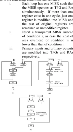
Definition 4. An RTL circuit is called reduced BIST- able if the following conditions are satisfied:
i. Each loop has one MISR such that the MISR operates as TPG and RA simultaneously. If more than one register exist in one cycle, just one register is modified into MISR and the rest of original registers are remained as unmodified register. ii. Insert a transparent MISR instead
of condition i, in case the cost of area overhead of condition ii is lower than that of condition i. iii. Primary inputs and primary outputs
are modified into TPGs and RAs respectively.
Fig. 3. (a) Original circuit (b) Reduced BIST-able RTL circuit with MISR register T5 and MISR register T6 in each loop. (c) Reduced BIST-able RTL circuit with one transparent MISR register T7. Example 4. Fig. 3 shows two types of reduced BIST- able RTL circuit. Fig. 3(b) shows reduced BIST-able with a MISR for each loop and Fig. 3(c) shows reduced BIST-able with a transparent MISR. Note that, the original register R2 is modified into MISR
register T5 and original register R3 is modified into MISR T6 in Fig. 3(b). We also can insert only a transparent MISR T7 at the sharing path of both loops to make the circuit self-testable as shown in Fig. 3(c). Regarding the cost, we choose the lower one between these two types.
Concurrent BIST-able RTL and reduced BIST- able RTL have different ways to break each loop in the circuit. Concurrent BIST-able RTL circuit breaks a loop with CBILBO while reduced BIST-able RTL circuit breaks a loop with a MISR. The cost of CBILBO is more expensive than the cost of MISR. Since we can reduce the cost and area overhead by using a MISR, so we call our approach reduced BIST-able RTL circuit. We also can get shorter test application time because we test all combinational blocks simultaneously and get comparable high fault coverage likes approach in [2].
3. DFT for Reduced BIST-able RTL circuit This section describes the DFT method that augments a given RTL into a reduced BIST-able RTL circuit. In the DFT, primary inputs and primary outputs are modified into TPGs and RAs respectively.
3.1 Problem Formulation
A reduced BIST-able RTL circuit has a MISR in each loop. The DFT for the reduced BIST-able RTL circuit is formalized as the following optimization problem.
o Input : a given RTL circuit
o Output : a reduced BIST-able RTL circuit o Optimization : minimizing area overhead 3.2 DFT algorithm
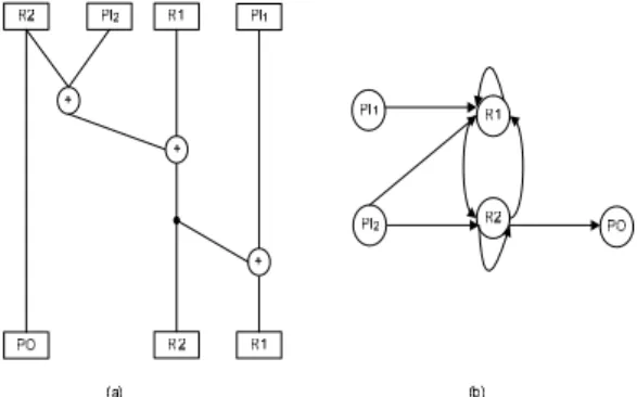
In order to augment a given RTL circuit into reduced BIST-able RTL circuit, we introduce an extended R- graph and an extended minimum feedback vertex set. We first look at definition of R-graph of ADD.
Definition 5. An R-graph of an ADD is a directed graph G=(V,A,w,) that has the following properties.
i. v∈V is a read node or write node. If a read node and a write node correspond to the same variable, they are represented by the same vertex;
ii. (vi, vj)∈A denotes an arc if there exists a path from the read node vi to the write node vj;
iii. w:V→Z+ (the set of positive integers) defines the size of read or write node corresponding to a vertex in V;
Fig. 4 (a) ADD for original RTL circuit S1 (b) R- graph for ADD S1
Example 5. Fig. 4(a) shows the R-graph of S1. Each read node and write node S1 are represented by input vertex and output vertex respectively in R-graph. Each path from read node to write node in ADD is represented by the arc from input vertex to output vertex in R-graph.
We define an extended R-graph as follows. An extended R-graph has an extra vertex called dummy vertex D. This dummy vertex represents an extra register as transparent register. These steps below are taken to construct an extended R-graph.
1. Transform an RTL circuit into an ADD representation.
2. Find the path such that dummy D is added into that path. Dummy D is added if there is a path between 2 operator nodes or a path between an operator node and a fan out node.
3. Construct an extended R-graph by replacing the read node, write node and dummy node in ADD into input vertex, output vertex and dummy vertex respectively in extended R- graph.
Definition 6. An extended R-graph of an ADD is a directed graph G=(V,A,w,) that has the following properties:
i. v∈V is a read node, write node or dummy node. If a read node and a write node correspond to the same variable, they are represented by the same vertex;
ii. (vi, vj)∈A denotes an arc if there exists a path from the read node vi to the write node vj,
iii. (vi, vn)∈A denotes an arc if there exists a path from the read node vi to the dummy vn iv. (vi, vm)∈A denotes an arc if there exists a path from the dummy vi to the dummy vk v. (vi, vs)∈A denotes an arc if there exists a
path from the dummy vi to the write node vs
vi. w:V→Z+ (the set of positive integers) defines the size of read, write node or dummy node corresponding to a vertex in V;
Fig. 5 (a) ADD for modified original circuit with dummy S2 (b) An extended R-graph for S2 Example 5. Fig. 5(b) shows an extended R-graph for S2. An extended R-graph has a cost for each vertex except the primary input and primary output vertex. In other words, cost means the area overhead of each vertex. The original register vertex represent as R1 and R2 and the dummy vertex represent as D1 until D3. In this case, since we modify the original register into MISR or transparent MISR to make this original circuit self-testable, so the each cost of R1 and R2 are 5 and the each cost of D1, D2 and D3 is 12. Note that, S2 modified with dummy D1, D2 and D3 in some paths. For example, D1 is added because there is a path between 2 operation nodes.
Definition 7. Minimum feedback vertex set is a set of vertices, V such that:
i. The number of vertices is minimized. ii. Every loop is broken by a vertex in a set of
vertices, v∈V.
Minimum feedback vertex set considers only the minimum number of vertex set that breaks every loop.
Example 6. Refer to Fig. 4(b), the minimum feedback vertex set is {R1, R2} because when R1 and R2 removed from the circuit, every loop is broken. Moreover, the circuit becomes acyclic when removing R1 and R2.
We define an extended minimum feedback vertex set so that the extended minimum feedback vertex considers the cost of feedback vertex set in our reduced BIST-able RTL circuit.
Definition 8. An extended minimum feedback vertex set is a set of vertices V such that:
i. Every loop is broken by a vertex in a set of vertices, v∈V.
ii. The summation cost of set of vertices that break a loop is minimized ∑ cost (v).
v∈V By introducing the extended minimum feedback vertex set, we consider the minimized cost of summation vertices set. Cost of summation vertices set is a total area overhead of vertices in a set of vertices. The set of vertices are divided into two sets. There are set of dummy vertex and set of original register vertex. For each vertex in the extended R- graph, we define cost p(v) for dummy vertex and original register vertex as follows.
i. Each cost of original register vertex p(v) = 5wr
ii. Each cost of dummy vertex p(v) = 12wd
We total up the cost of vertex in the dummy vertex set and original register dummy set and find the minimum total cost for both vertex sets. Then, we choose the minimum one. If the minimum summation cost belongs to an original register vertex set, therefore, we replace each vertex of that sets with MISR. However if the minimum summation cost belongs to a dummy vertex set, we replace each vertex of that sets with transparent MISR.
Example 7. Refer to Fig. 5(b), we find the two sets of feedback vertex set. There are original register vertex set and dummy vertex set. The minimum feedback vertex sets for original register vertex is {R1,R2} and the minimum feedback vertex sets for dummy vertex is {D2}. Since the summation cost of {R1,R2} is 10 where the cost of each R1 and R2 is 5 and the summation cost of {D2} is 12, we choose the set of {R1,R2} as extended minimum feedback vertex set because the summation cost of the set of {R1,R2}is lower than and the summation cost of {D2}. Therefore, we modify the RI and R2 into MISR to make the circuit testable.
4. CASE STUDIES
4.1 Experiment Setup
In the case studies, we evaluated the effectiveness of the proposed method by performing fault simulation on the circuits augmented with the proposed BIST method. Experiments have been conducted on ITC’99 benchmark circuits where the behavioural descriptions are given. We compared reduced BIST- able RTL circuit with primitive BIST-able RTL circuit and concurrent BIST-able RTL circuit
(Wunderlich’s method [2]). Table 1 presents the characteristic of the benchmark circuits. In Table 1,
#FF represents the number of flip-flops while PI/PO represents the number of inputs/outputs of the circuit. The area column represents the area of the circuit where one unit of area is equal to the size of an inverter.
Table 1. Characteristics of the benchmark circuits
4.2 Experimental Results
We evaluated the effectiveness of the circuits in terms of fault coverage, area overhead and test application time. We compared our method with concurrent BIST-able RTL circuit and primitive BIST-able RTL circuit. Figs. 6-12 show the results of fault coverage versus clock cycles. Since the test patterns generated by MISR for a combinational block partly depend on the test responses from the preceding combinational block, some of the random test patterns cannot be generated. Because there are not many useful random test patterns missed by the MISR, the fault coverage of our method is just slightly lower than that of concurrent BIST-able RTL circuit. For benchmark circuit such as b02, our method obtains 88% while 90% using concurrent BIST-able RTL circuit after 100 clock cycles. We determine the clock cycles first then find out what fault coverage based on that clock cycles.
Table 2 represents the percentage of the area overhead compared to the area of primitive BIST- able RTL circuit. Our method shows that all the benchmark circuits have lower area overhead compared to concurrent BIST-able RTL circuit. Refer to circuit b02 in Table 2, only one register called stato that has 3 bits is modified into CBILBO and MISR. By modifying register stato into CBILBO and MISR, it needs 51% area overhead and 22% area overhead respectively. We modify the original register into MISR at behavioural descriptions to make RTL circuit BIST-able such that the area overhead becomes low.
Fig. 6 b01 circuit
Fig. 7 b02 circuit
Fig. 8 b03 circuit
ITC’99 # Flip-flops Area IO pins
PI PO
b01 5 90 4 2
b02 4 63 3 1
b03 30 422 6 4
b06 9 138 4 6
b09 28 391 3 1
b10 17 341 13 6
Fig.9 b06 circuit
Fig.10 b09 circuit
Fig.11 b10 circuit
5. Conclusions
A new BIST technique for test-per-clock scheme has been introduced in this paper. A given RTL circuit augmented by our DFT method is called reduced BIST-able RTL circuit. We modify the original register into MISR at behavioural descriptions to make RTL circuit BIST-able. Our method shows
high fault coverage and lower area overhead for the ITC’99 benchmark circuits compared to concurrent BIST-able RTL circuit and primitive BIST-able RTL circuit.
Table 2. Area overhead
REFERENCES
[1] M. Abramovici, M. A. Breuer, and A.D.Friedma: Digital Systems Testing and Testable Design, Computer Science Press (1990).
[2] A. P. Stroele and H. J. Wunderlich: “Hardware-optimal test register insertion,” IEEE Trans. on Computer-Aided Design of Integrated Circuits and Systems, 17(6):531–539 (1998).
[3] T.Masuzawa, M.Idutsu, H.Wada,and H.Fujiwara:
“Single-control testability of RTL data paths for BIST,” Proc. 9th Asian Test Symposium, pp.210-215(2000). [4] K. Yamaguchi, H.Wada, T. Masuzawa, and H.Fujiwara:”A BIST Method Based on Concurrent Single- Control testability of RTL data paths for BIST,” Proc. 10th Asian Test Symposium, pp.313-318(2001).
[5] Kenichi Yamaghuci, Michiko Inoue, Hideo Fujiwara:
“Test-per-clock BIST with low overhead,” 2007 Wiley Periodicals, Inc. Electronics and Communications in Japan Pt 2, volume 90, Issue 6, pp.47–58, (2007).
[6] B.Koenemann, J.Mucha,and G.Zwiehoff:”Built-in logic block observation techniques,” In IEEE Test Conf., pp.37- 41(1979).
[7] I. Ghosh, N. K. Jha, and S. Bhawmik: “A BIST scheme for RTL controller-data paths based on symbolic testability analysis,” In Proc. Design Automation Conf., pp. 554–559 (1998).
[8] K. Kim, D.S. Ha and J.G. Tront, “On using signature registers as pseudorandom pattern generators in built in self testing,” IEEE Trans. Computer-Aided Design,pp, 919-928, August 1988.
ITC’99 Primitive BIST-able
Concurrent BIST-able [2]
Reduced BIST-able [proposed method ] Area
(OH%)
Area (OH%)
Area (OH%) b01 90(0%) 154 (71%) 107 (19%) b02 63(0%) 95 (51%) 77 (22%) b03 422(0%) 589 (40%) 449 (6%) b06 138(0%) 208 (51%) 161 (17%) b09 391(0%) 612 (75%) 437 (12%) b10 341(0%) 383 (12%) 359 (5%)