Identifying Non-Robust Untestable RTL Paths in Circuits with
Multi-Cycle Paths
Thomas Edison Yu Tomokazu Yoneda Satoshi Ohtake and Hideo Fujiwara
Graduate School of Information Science, Nara Institute of Science and Technology 8916-5 Takayama-cho, Ikoma City, Nara, 630–0101, Japan
E-mail:{tomasu-y, yoneda, ohtake, fujiwara}@is.naist.jp
Abstract
As LSI manufacturing technology improves and the time-to- market for products becomes stricter, more and more circuit designs have multiple clock domains due to concerns such as design re-use, power reduction and temperature control. It is not uncommon for these designs to have multi-cycle paths which are untestable. The rapid identification of these untestable paths reduces test generation time as well as over-testing due to design for testability (DFT). For current and future designs, this has already become impractical at the gate-level. This paper presents a method to identify non- robust untestable multi-cycle paths at the register transfer level (RTL) and the details in a case study of a benchmark circuit.
Keywords
false path identification, non-robust test, register transfer level, multi-cycle path
1. INTRODUCTION
Efficient identification of path delay faults (PDF) has be- come an important topic as chip timing requirements be- come stricter and delay testing and analysis become more important. Generally, DFT techniques are used to reduce test cost. However, they introduce over-testing problems since DFT techniques can make untestable paths testable. Therefore, rapid and correct untestable path identification has become a requirement to reduce automatic test pattern generation (ATPG) time as well as yield loss from over- testing when applying DFT to chip designs [8]. Several efficient methods have already been proposed for untesta- ble path identification for combinational circuits at the gate- level[2-4]. Untestable PDF identification for sequential circuits have been addressed in [5], also at gate-level. However, with today’s complex chip designs, complete untestable path identification at the gate-level has become unfeasible, especially for sequential circuits[5]. Consider- ing the great number of gate-level paths, [8] presented a way to identify untestable paths at RTL for sequential cir- cuits. At RTL, the number of paths to be analyzed is greatly reduced and if the correspondence of RTL paths to gate- level paths can be established, a great reduction to ATPG time can be gained.
Chip designs can have multi-cycle paths which can be due to resource sharing, multiple clock domains for low-power designs and IP re-use as well. Thus, the identification of multi-cycle untestable paths has increasingly become an important problem for reducing ATPG time and test size [10]. [6, 7, 9, 10] have presented several techniques for multi-cycle path identification. More specifically, [10] stud- ied the effects of multi-cycle false path removal on testabil- ity while [7] aimed to derive the valid clock period of a circuit using gate and segment delay information. [9] spe- cifically addressed the problem of reducing test generation and fault grading time. However, all of these approaches for multi-cycle untestable path identification only consid- ered gate-level circuits.
In this paper, we present sufficient conditions for rapid and efficient identification of non-robust untestable multi-cycle paths at RTL. Although, untestable path identification at RTL was first introduced in [8], the authors only consid- ered single-cycle RTL untestable paths and ignored the possibility that some paths may not be untestable if tested at more than one clock cycle. In this paper, we increase the quality of the identified false paths compared to [8]. For the rest of this paper, non-robust untestable paths will be re- ferred to as false paths as in [8].
The contributions of this paper are: (1) introduce the con- cept of multi-cycle false paths at RTL, (2) derive sufficient conditions for multi-cycle RTL false paths for two transi- tion propagation models which can be modified to apply to various circuit designs, and (3) give a case study of a benchmark circuit which proves the necessity of identifying
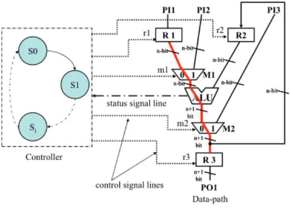
Figure 1. Example RTL circuit
R 1
ALU 0 1 m1
PI2
n-bit n-bit n-bitn-bit
n-bit n-bit
n-bit n-bit
n+1 bit n+1
bit
PI3
0 1 m2
R 3
n-bit n-bit
PI1
PO1
n+1 bit n+1 bit n+1 bit n+1 bit
S0
S1
Si
Controller
Data-path
r1 r2 R2
r3 status signal line
control signal lines
n-bit n-bit
M1
M2
17th Asian Test Symposium 17th Asian Test Symposium
multi-cycle false paths as well as show the effectiveness of our method.
The rest of this paper is organized as follows. Preliminary ideas and assumptions are given in Section 2. Multi-cycle RTL false path identification is explained in Section 3. Sec- tion 4 presents a case study about using applying the condi- tions in Section 3 on a benchmark circuit, while Section 5 concludes this paper.
2. PRELIMINARIES 2.1 RTL Circuits
The method presented in this work uses RTL information to quickly identify false paths. The RTL circuits under con- sideration are represented as a structural design consisting of a controller (finite-state machine), a datapath (made up of multiplexers (MUXs), registers, and other RTL combina- tional modules), and the corresponding RTL signal lines (control and status signals) connecting them as shown in Figure 1.
For this work, we only consider designs with a single clock domain, and RTL paths in datapaths. We assume that, for controllers, there exists no multi-cycle paths, and state tran- sitions are completely specified for each possible state and input vector pair. We also assume that delay information for the modules and segments are not available at RTL. 2.2 RTL Path
An RTL path is a path which starts at a primary input (PI) or a register (start register Rs) and ends at a primary output (PO) or register (end register Re). Furthermore, it must only pass through combinational modules and can represent one or a bundle of single-bit paths. For example, a path from register R1 passing through multiplexer M1, the ALU, mul- tiplexer M2 and ending at register R3 in Fig. 1 is consid- ered an RTL path. Since each RTL path can represent a bundle of gate-level paths, after logic synthesis, these RTL paths are transformed into a large number of gate-level paths. However, the final gate-level circuit configuration greatly depends on the type of logic synthesis used. In order
to achieve RTL path to gate-level path correspondence, we restrict logic synthesis to a module interface preserving- logic synthesis (MIP-LS) as defined in [8]. In MIP-LS, each RTL module is transformed into individual gate-level netlists. Since optimizations are only performed within each module and each RTL signal line connecting the modules are split into 1-bit signal lines, the connection configuration in-between the modules are guaranteed to be preserved and propagated to the gate-level synthesized circuit.
2.3 Single-cycle RTL False Path
At gate-level, false paths are paths which cannot be sensi- tized by any input vector.
Definition 1: RTL False Path
RTL false paths are RTL paths whose corresponding gate- level paths are all false for any logic synthesis[8].
Although RTL false paths were first defined in [8], the au- thors only presented sufficient conditions for single cycle RTL false paths.
Theorem 1: An RTL path is single-cycle RTL false w.r.t. MIP-LS if it satisfies one of the following conditions at any time t:
1. No transition occurs at the starting point of the path at time t.
2. Any transition at the starting point at time t is not propagated along the path to the end point within one clock cycle.
3. No value is captured at the ending point at time t+1. 4. No value captured at the ending point of the path at
time t+1 is ever propagated to any PO. 3. MULIT-CYCLE RTL FALSE PATH
IDENTIFICATION 3.1 Multi-Cycle RTL Path
Multi-cycle RTL paths are essentially RTL paths which don’t need to finish propagating a signal from a starting point to its end point within one clock cycle.
Definition 2: k-cycle RTL Path Figure 2. Example multi-cycle RTL path
R 1
ALU 0 1 m1=0
PI2 PI3
m2 PI1
PO1
r1=H r2 R2
r3 R 3 0 1
R 1
ALU 0 1
PI2 PI3
m2=0 PI1
PO1 r2 R2
r3 R 3 0 1 r1=H
m1=0 R 1
ALU 0 1 m1
PI2 PI3
m2 PI1
PO1
r1=L r2 R2
r3 R 3 0 1
t t + 1 t + 2
M1
M2
M1
M2 M1
M2
A multi-cycle RTL path which has up to k clock cycles to propagate a transition from source to destination.
Assume that the RTL circuit shown in Figure 2 has a 3- cycle RTL path from R1 passing through multiplexer M1, the ALU, multiplexer M2 and ending at register R3. At time t, the control signal of R1, r1, is set to L and R1 loads a value from primary input PI1. At t+1, this transition is propagated through the path and reaches the ALU within 1 clock cycle. At t+2, the transition continues to propagate from the ALU until it reaches the input of R3. While not shown, the control signal of R3, r3, becomes L at t+3 and the transition is captured.
3.2 k-Cycle RTL False Path
At gate-level, k-cycle false paths are paths which cannot be sensitized by any input vector within k clock cycles. Definition 3: k-Cycle RTL False Path
A k-cycle RTL false path is an RTL path whose corre- sponding gate-level paths are all k-cycle false for any logic synthesis.
Theorem 2: An RTL path is k-cycle false w.r.t MIP-LS if it satisfies one of the following conditions at any time t:
1. No transition ever occurs at the start register, Rs, or PI of the RTL path at time t.
2. Any transition at the starting point of the path at time t is never propagated along the path to the ending point within k clock cycles.
3. No value is captured at the ending point at time t+k.
4. No value captured at the ending register, Re, at time t+k is ever propagated to any PO.
The proof for Theorem 2 is just a simple extension of the proof for Theorem 1 and is omitted in this paper. RTL paths which are k-cycle RTL false for k҈2 are multi-cycle RTL false paths. Furthermore, if a path is k-cycle RTL false for any value of k, it is only then that we can consider it as an RTL false path.
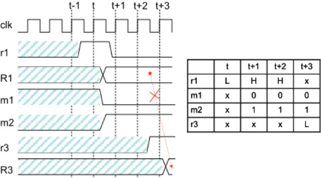
3.3 Control-Dependent k-Cycle RTL False Path At RTL, we can determine information regarding state tran- sitions and control signals (i.e. Load / Hold signals, MUX select signals, etc.) given a state and input vector pair. We can therefore define sufficient conditions for identifying k- cycle RTL false paths using the control signal information. k-cycle false paths identified this way are called control- dependent k-cycle false (CDkF) paths. For this work, we will only consider paths starting at datapath registers (DR) or PIs and ending at datapath registers (DR) or POs. An example of a CDkF RTL path is shown in Figure 3. Assuming that the timing diagram and control signal table of the path specified in Figure 2 is the only possible control sequence at any time t, the path starting from R1 to R3 passing through MUX M1, an ALU, and MUX M2 is CDkF at k=3 if we consider the timing diagram for the con-
R3 (r3) from time t to t+3 (the variables in parentheses are the respective control signals per module). The table shows the effective control signal at each clock edge, where L means a LOAD signal, H represents a HOLD signal, num- bers represent the selected input of a multiplexer, and x’s represent signal values which can be ignored at each time frame. At time t, r1=L and R1 loads a new value. This value is then propagated through M1 (m1 selects the on- path) within 3 clock cycles. Unfortunately, while R3 has a load signal at t+3, M2 never selects the on-path (m2 must be 0 in order to propagate the transition) from t+1 to t+3 and blocks the propagation of the signal from M1. There- fore, judging from the control signals from t to t+3, the path is 3-cycle CDkF.
The specific definition of a multi-cycle path can vary ac- cording to the design rules being followed by the circuit designers. For example, an RTL path will be classified dif- ferently depending on whether it belongs to a non-pipelined, pipelined or wave-pipelined circuit. For this work, we pre- sent solutions for a simple and strict single-transition cir- cuit model and a less-strict, generalized model which are applicable to many circuit designs. Each transition propaga- tion model and their corresponding sufficient conditions for CDkF RTL path identification are discussed in the follow- ing subsections. Note that these two models represent ex- treme cases and can be easily modified to reflect other cir- cuit designs.
3.3.1 Single-transition Circuit Model
In the single-transition model, the k-cycle paths of a circuit must exhibit the following characteristics at any time t:
1. When the start register, Rs, loads at t, it must hold the value from t+1 to t+k.
2. All multiplexers on the path must continuously se- lect the on-path from t+1 to t+k.
3. The end register Re must load at t+k.
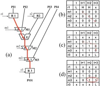
In short, given a k-cycle path, only the transition from Rs at time t is ever propagated to Re within k clock cycles. An example control sequence table of a 3-cycle path that can be a true path is shown in Figure 4(a) for the path given in Fig. 2. For the transition to propagate from R1 to R3, it is imperative that all the multiplexers select the on-path from
clk
t t+1 t+2 t+3 t-1
r1 R1 m1 m2 r3 R3
x 1 0 H t+2
L x
x r3
1 1
x m2
0 0
x m1
x H
L r1
t+3 t+1
t
x 1 0 H t+2
L x
x r3
1 1
x m2
0 0
x m1
x H
L r1
t+3 t+1
t
Figure 3. Example 3-cycle CDkF path timing
t+1 to t+3. In contrast, in Fig. 4(b), R1 loads a new value at t+2 while in Fig. 4(c), the multiplexer M1 selects an off- path at t+2. Both of these situations violate the require- ments for single-transition propagation through the target path.
To derive sufficient conditions for false path identification under the single-transition model, we first introduce the concept of register controllability and observability. Regis- ter controllability denotes the capability of triggering a tran- sition on a register while register observability denotes the capability of propagating the transition from a register to a PO.
Definition 4: Register Controllability for Single- transition Model
Let P be the set of paths ending at register R. R is uncon- trollable at time t if it satisfies one of the conditions below for every path q ∈ P for any v≥1:
1. No control sequence for the starting register, Rs, of q starting from t-v to t is of the form {LHv-1x} or Rs is uncontrollable at time t-v.
2. R does not load at time t.
3. Let oMi be the control signal which selects the on-path for each multiplexer Mi in q (1҇i҇n and n is the num- ber of multiplexers in q). No control sequence for each Mi is of the form {xvoMi} from t-v to t.
Definition 5: Register Observability for Single- transition Model
Let P be the set of paths starting at R. R is unobservable at time t if it satisfies one of the conditions below for every path q ∈ P for any v≥1:
1. No control sequence for R starting from t to t+v is of the form {LHv-1x}.
2. The end register, Re, does not load at time t+v or Re is unobservable at time t+v.
3. Let oMi be the control signal which selects the on-path for each multiplexer Mi in q (1҇i҇n and n is the num- ber of multiplexers in q). No control sequence for each Mi is of the form {xvoMi} from t to t+v.
Theorem 3: RTL CDkF paths for Single-transition Model
An RTL path p is RTL CDkF with respect to the single- transition model and MIP-LS if one of the following 3 con- ditions is satisfied at any time t:
1. Given the set of all possible control signal sequences of the start register Rs for k clock-cycles, a control se- quence of the form {LHk-1x} starting at time t cannot be found or Rs is uncontrollable at t.
2. Let oMi be the control signal which selects the on-path for each multiplexer Mi in p (1҇i҇n and n is the num- ber of multiplexers in p). No control sequence for each Mi is of the form {xoMi
k} from t to t+k..
3. The transition is not captured by Re at t+k or Re is unobservable at t+k.
3.3.2 Generalized Model
We further extend our methodology to consider the “possi- bility” of a transition starting from the Rs of a k-cycle RTL path to be propagated to its Re within k-clock cycles re- gardless of whether or not Rs continuously holds the value and/or all the MUXs continuously select the on-path. Here, as long as there is a possibility for a transition to be propa- gated within k-clock cycles, we cannot consider it to be CDkF. As an example, consider the control sequence table in Figure 5(c) for the RTL path in Fig. 5(a), where a transi- tion propagation path can be found from M1 to M3 because the transition could have passed through M1 at t+1 even though m1 selected the off-path during the subsequent cy- cles, it could also have passed through M2 and M3 at t+3 and finally captured by R3 at t+3. In contrast, M3 com- pletely blocks the propagation of the transition from M2 to R3 at t+2 to t+3 in Fig. 5(d). Note that successful transition propagation w.r.t. the single-transition model (Fig. 5(b)) also means possible success w.r.t. the generalized model but not vice versa. Also, a path that violates the conditions
Figure 5. Comparison of single-transition model and generalized model
0 0 0 x m3
x 0 0 H t+2
L x x r3
0 0 x m2
0 0 x m1
x H L r1
t+3 t+1 t
0 0 0 x m3
x 0 0 H t+2
L x x r3
0 0 x m2
0 0 x m1
x H L r1
t+3 t+1 t
0 1 1 x m3
x 1 1 x t+2
L x x r3
0 1 x m2
1 0 x m1
x x L r1
t+3 t+1 t
0 1 1 x m3
x 1 1 x t+2
L x x r3
0 1 x m2
1 0 x m1
x x L r1
t+3 t+1 t
1 1 0 x m3
x 0 0 x t+2
L x x r3
0 1 x m2
0 0 x m1
x x L r1
t+3 t+1 t
1 1 0 x m3
x 0 0 x t+2
L x x r3
0 1 x m2
0 0 x m1
x x L r1
t+3 t+1 t
(b)
(c)
(d)
(a)
R 1
ALU 0 1 m1
PI2 PI3
m2 PI1
PO1
r1 r2 R2
r3 0 1
R 3 M1
M2
m3 0 1 M3
PI4
x 0 0 H t+2
L x
x r3
0 0
x m2
0 0
x m1
x H
L r1
t+3 t+1
t
x 0 0 H t+2
L x
x r3
0 0
x m2
0 0
x m1
x H
L r1
t+3 t+1
t
x 0 1 H t+2
L x
x r3
0 0
x m2
0 0
x m1
x H
L r1
t+3 t+1
t
x 0 1 H t+2
L x
x r3
0 0
x m2
0 0
x m1
x H
L r1
t+3 t+1
t
x 0 0 L t+2
L x
x r3
0 0
x m2
0 0
x m1
x H
L r1
t+3 t+1
t
x 0 0 L t+2
L x
x r3
0 0
x m2
0 0
x m1
x H
L r1
t+3 t+1
t
(a)
(b) (c)
Figure 4. (a) Possible 3-cycle testable path, (b)(c) 3-cycle CDkF w.r.t. the single-transition
d l
for the generalized model automatically violates the single- transition model but not vice versa.
Definition 6: Register Controllability for Generalized Model
Let P be the set of paths ending at register R. R is uncon- trollable at time t if it satisfies one of the conditions below for every path q ∈ P for any v≥1:
1. No control sequence for the starting register, Rs, of q starting from t-v to t is of the form {Lxv} or Rs is un- controllable at time t-v.
2. R does not load at time t.
3. Let oMi be the control signal which selects the on-path for each multiplexer Mi in q (1҇i҇n and n is the num- ber of multiplexers in q). No control sequence for each Mi is of the form {xWioMixv-Wi} from t-v to t, where 1≤ Wi≤ v, Wi-1≤ Wi and 2҇i҇n.
Definition 7: Register Observability for Generalized Model
Let P be the set of paths starting at register R. R is unob- servable at time t if it satisfies one of the conditions below for every path q ∈ P for any v≥1:
1. No control sequence for R starting from t to t+v is of the form {Lxv}.
2. The end register, Re, of q does not load at time t+v or Re is unobservable at time t+v.
3. Let oMi be the control signal which selects the on-path for each multiplexer Mi in q (1҇i҇n and n is the num- ber of multiplexers in q). No control sequence for each Mi is of the form {xWioMixv-Wi} from t to t+v, where 1≤ Wi≤ v, Wi-1≤ Wi and 2҇i҇n.
Theorem 4: RTL CDkF paths for Generalized Model An RTL path p is RTL CDkF with respect to the general- ized model and MIP-LS if one of the following 3 condi- tions is satisfied at any time t:
1. Given the set of all possible control signal sequences of the start register, Rs, for k clock-cycles, a control se- quence of the form {Lxk} cannot be found or Rs is un- controllable at t.
2. Let oMi be the control signal which selects the on-path for each multiplexer Mi in p (1҇i҇n and n is the number of multiplexers in p). No control sequence for each Mi is of the form {xWioMixk-Wi} from t to t+k, where 1≤ Wi≤ k, Wi-1≤ Wi, and 2҇i҇n.
3. The transition is not captured by Re at t+k or Re is unobservable at t+k.
4. CASE STUDY 4.1 Problem Definition
In this subsection, we formally define the RTL CDkF path identification problem PCDKF:
Given an RTL circuit CRTL, its corresponding transition propagation model and k, determine the RTL CDkF paths in the datapath of CRTL.
Bit width
#PIs #POs #REGs #States #RTL paths
8 3 2 6 4 19
4.2 Using the LWF Benchmark Circuit
As a case study, we have opted to apply the conditions for RTL CDkF path identification for both transition propaga- tion models on a Lattice Wave Filter (LWF) [8] benchmark circuit. The characteristics (bit width, number of PIs, POs, Registers, States and RTL paths) of the LWF circuit are shown in Table 1. Note that for this case study, we ignored the presence of the RESET input as well as the reset func- tion of the circuit. Thus, the state transition of the circuit is simplified into the various sequences formed by the four possible circuit states.
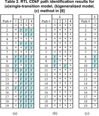
Applying the sufficient conditions for RTL CDkF identifi- cation w.r.t. the single-transition model, we get the results shown on Table 2(a). In Table 2(a), the classification of each of the 19 RTL paths is shown with respect to the value of k, where those marked “F” are CDkF at that value of k. An asterisk means there is no definite conclusion, and thus the path might be testable at that value of k. As we have expected, there are paths whose testability will vary accord- ing to the value of k. For example, path #10 is single cycle untestable, but it might be testable at k=2. If we only use the method in [8], this possibility would have been ignored and the path would be immediately considered false. Paths
#3 and #6, on the other hand, might be testable at both k=1, 2. It is reasonable to conclude that the paths must be tested at both cycle counts unless the designer specifies other wise. Another interesting result is that for paths #1, #4, #7 which show that these paths are testable up to k=4. Finally, paths
#8, #9, #11 and #15 were all false for all values of k. If the circuit designer states the maximum value of k to be 4, then we can consider these paths as RTL false w.r.t. the design constraints of the circuit.
The CDkF identification results w.r.t. the generalized model is shown in Table 2(b). As expected, the number of identified false paths is much less compared to the single- transition model. It must be noted that the single-transition model can be considered as a special case of the general- ized model, and thus paths that are not considered false in Table 2(a) are also classified in the same way in Table 2(b). Note that while paths #8 and #9 are considered untestable for all the allowed values of k under the single-transition model, the generalized model considers the possibility that they are testable at values of k>1. Furthermore, paths that are false in Table 2(a) for all k, such as paths #11 and #15, can possibly be testable for all k under the generalized model.
Comparing the results using the method in [8] for single- cycle RTL paths shown in Table 2(c) to Table 2(a), we can
Table 1. Characteristics of the LWF circuit
see that the number of identified false paths has increased. The authors of [8] have confirmed that there was a mistake in the table of results presented in [8] and that their updated results are identical to that in Table 2(a) for k=1. Further- more, the possibility of path #10 being testable at k=2 under the single-transition model and testable at k=4 under the generalized model is completely ignored in [8]. This shows that an increase in the resolution of path identification, and therefore, an increase in test quality can be achieved if we consider multi-cycle RTL false paths. Note that the results would also vary depending on the transition model used, and both models that are presented in this paper represent polar extreme cases.
5. CONCLUSION
In this paper, we have introduced the concept of multi-cycle false paths at RTL and derived delay-independent sufficient conditions for multi-cycle RTL false path identification for two transition propagation models. Furthermore, these models and conditions can be easily modified to apply to various circuit designs. The case study has shown that paths can be classified as false or not depending on the transition propagation model used as well as the number of clock cycles allowed per test. Thus, there is no doubt that if multi-cycle paths exist in a circuit, they should be classified and tested appropriately. As was shown in [8], rapidly iden- tifying RTL false paths can increase test efficiency and quality and reduce ATPG time and over-testing. It can be concluded that extending the path analysis to cover multi- cycle RTL paths can further increase the test quality and efficiency.
6. ACKNOWLEDGMENTS
The authors would like to thank Prof. Yuki Yoshikawa and Prof. Tomoo Inoue of the Hiroshima City University, Prof. Michiko Inoue and the members of Computer Design and Test Laboratory of the Nara Institute of Science and Tech- nology for their valuable comments. This work was sup- ported in part by Semiconductor Technology Academic Research Center (STARC) under the Research Project and in part by Japan Society for the Promotion of Science (JSPS) under Grants-in-Aid for Scientific Research B (No. 20300018).
7. REFERENCES
[1] A. Krstic and K.T. Cheng, Delay Fault Testing for VLSI Circuits, Kluwer Academic Publishers, 1998. [2] K.T. Cheng and H.C. Chen, “Classification and Identi-
fication of Nonrobust Untestable Path Delay Faults,” IEEE Trans. Computer-Aided Design of Integrated Circuits and Systems, vol. 15, no. 8, pp. 854–853, Aug. 1996.
[3] S. Kajihara, K. Kinoshita, I. Pomeranz, and S.M. Reddy, “A Method for Identifying Robust Dependent and Functionally Unsensitizable Paths,” Proc. Interna- tional Conference on VLSI Design, pp. 82–87, 1997. [4] S.M. Reddy, S. Kajihara, and I. Pomeranz, “An Effi-
cient Method to Identify Untestable Path Delay Faults,” Proc. of 10th Asian Test Symposium, pp. 233– 238, Nov. 2001.
[5] A. Krstic, S.T. Chakradhar, and K. T. Cheng, “Testable Path Delay Fault Cover for Sequential Circuits,” Proc. of European Design Automation Conference, pp. 220– 226, Sep. 1996.
[6] W.C. Lai, A. Krstic, and K.T. Cheng, “On Testing The Path Delay Faults of a Microprocessor Using Its In- struction Set,” Proc. of 18th VLSI Test Symposium, pp. 15–20, May 2000.
[7] K. Yang and K.T. Cheng, “Efficient Identification of Multi-Cycle False Path,” Proc. of Conference on Asia South Pacific Design Automation, pp. 360–365, 2006. [8] Y. Yoshikawa, S. Ohtake and H. Fujiwara, “False Path
Identification using RTL Information and Its Applica- tion to Over-testing Reduction for Delay Faults,” Proc. of 16th Asian Test Symposium, pp. 65–68, Oct. 2007. [9] M. Syal, M.S. Hsiao, S. Natarajan and S. Chakravarty,
“Untestable Multi-Cycle Path Delay Faults in Indus- trial Designs,” Proc. of 14th Asian Test Symposium, pp. 194-201, 2005.
[10] P. Kalla and M. Ciesielski, “Testability of Sequential Circuits with Multi-Cycle False Paths,” Proc. of 15th VLSI Test Symposium, pp. 322-328, 1997.
Table 2. RTL CDkF path identification results for (a)single-transition model, (b)generalized model,
(c) method in [8] k
Path # 1 2 3 4 1 * * * * 2 * F F F 3 * * F F 4 * * * * 5 * F F F 6 * * F F 7 * * * * 8 F F F F 9 F F F F 10 F * F F 11 F F F F 12 * F F F 13 * F F F 14 * F F F 15 F F F F 16 * F F F 17 * F F F 18 * F F F 19 * F F F
k Path # 1 2 3 4
1 * * * * 2 * * * * 3 * * * * 4 * * * * 5 * * * * 6 * * * * 7 * * * * 8 F * * * 9 F * * * 10 F * F * 11 * * * * 12 * * * * 13 * * * * 14 * * * * 15 * * * * 16 * * * * 17 * * * * 18 * * * * 19 * * * *
(a) (b) (c) k Path # 1
1 *
2 *
3 *
4 *
5 *
6 *
7 *
8 F
9 F
10 F 11 * 12 * 13 * 14 * 15 * 16 * 17 * 18 * 19 *