Delay Fault ATPG for F-Scannable RTL Circuits
Marie Engelene J. Obien, Satoshi Ohtake, and Hideo Fujiwara Graduate School of Information Science,
Nara Institute of Science and Technology, Japan E-mail: {obien-j, ohtake, fujiwara}@is.naist.jp
Abstract—Today’s digital circuits demand both high speed performance and miniaturization of chip size. As a result, delay fault testing has become very important to verify the quality requirements of VLSI chips. Full scan has been used to generate test patterns that achieves high fault coverage, of which the standard techniques for delay scan testing are skewed-load and broad-side. However, as the circuits become larger, using full scan can be very costly due to high area overhead and long test application time. In this paper, we apply delay fault automatic test pattern generation (ATPG) on F-scannable circuits. In our previous work [3], [4], we have shown the strengths of F- scan compared with full scan in terms of area overhead, test application time, and fault coverage. We utilize the advantages of F-scan to solve the current problems of skewed-load and broad-side. The proposed method is to utilize a hybrid model for F-scannable circuits in generating test patterns, wherein a fast scan enable signal used by skewed-load technique is not required. Transition delay fault coverage achieved by this approach is equal to or higher than that achieved by both skewed-load and broad- side approaches for gate-level full scan. This is proven through our experiments on ITC’99 benchmark circuits.
I. INTRODUCTION
The trend of decreasing transistor size and increasing clock speeds in today’s digital circuits require that the chips be tested to function correctly at certain desired speeds in order to ensure quality. However, the complexity of testing VLSI cir- cuits demand for methods that aid in producing functional test patterns with satisfactory fault coverage. Moreover, applying such test patterns at-speed for high speed circuits requires strict timing accuracy. These concerns result to very high costs of development and automatic test equipment (ATE). A popular solution is to utilize design-for-testability (DFT) techniques, of which full scan is most commonly used [1]. In fact, scan- based delay testing is increasingly utilized as a cost effective alternative to the at-speed functional pattern approach to test large scale chips for performance-related failures [5], [6]. In scan-based delay testing, test patterns are generated by an automatic test pattern generation (ATPG) engine on circuits with scan chains. In this work, we apply scan-based delay test using F-scan, which has a high fault coverage and is superior to full scan in terms of area overhead and test application time [3], [4]. F-scan organizes every register in the circuit in an F- scan-path by maximizing the use of available functional logic and paths to be used during scan, unlike gate-level full scan, which converts all flip-flops into scan flip-flops and connect them into a chain or multiple chains.
The difference of delay faults as compared to stuck-at faults is that, they cause errors in the functionality of a circuit based
on its timing. These faults are caused by the finite rise and fall times of the signals in the gates and the propagation delay of interconnects between the gates. One advantage of F-scan is the capability of its scan function to run at the same speed as its operation. This means that the same clock speed can be used during scan and normal mode, unlike in full scan wherein the scan mode is usually operated at slower speeds. Due to this, we can say that scan testing using F-scan is at-speed, which is possible because the F-scan-paths used for scan are integrated in the circuit at register-transfer level (RTL). Moreover, the F-scan-paths are synthesized with the circuit. Hence, timing, area, and performance are optimized for the circuit, which includes the F-scan-paths, during synthesis. This means that the structure of F-scannable circuits is built for effective delay scan testing.
In order to detect a delay fault, a pair of test patterns is usually required: the initialization pattern and launch pattern. The first pattern initializes the target faulty circuit line to a desired value. On the other hand, the second pattern launches a transition at the circuit line and propagates the fault effect to the primary output(s) and/or scan flip-flop(s). These two pat- terns are needed to detect transition faults: slow-to-rise faults and slow-to-fall faults [7]. Two approaches, namely, skewed- load[7] and broad-side[8], are utilized to apply two-pattern tests to standard scan designs. The next chapter describes how these approaches differ in the application of the second pattern of each pattern pair during delay scan testing.
In this paper, we propose a hybrid model of the F-scannable circuit for delay ATPG that achieves high fault coverage. This approach combines the advantages of both skewed-load and broad-side. A previous work by Wang [9] presented a hybrid delay scan method for full scan. Wang’s work chooses a small set of selected scan flip-flops to be controlled by the skewed- load approach and the rest are controlled by the broad-side approach. Although results show that their approach achieves higher fault coverage for most of the circuits compared with the broad-side approach, the fault coverage of skewed-load is still superior. High fault coverage for delay scan testing is important to ensure the quality of the circuit. Thus, our method aims to achieve fault coverage that is equal or higher to skewed-load approach for full scan, without the disadvantages of hardware cost and scan-enable timing difficulties.
Another inherent feature of our hybrid model for F- scannable circuits is the integrated constraint in the hybrid model such that the generated test patterns are functionally reachable states as much as possible. In this case, there is a
IEEE Int. Symp. on Communications and Information Technologies (ISCIT'10), pp. 717-722, Oct. 2010.
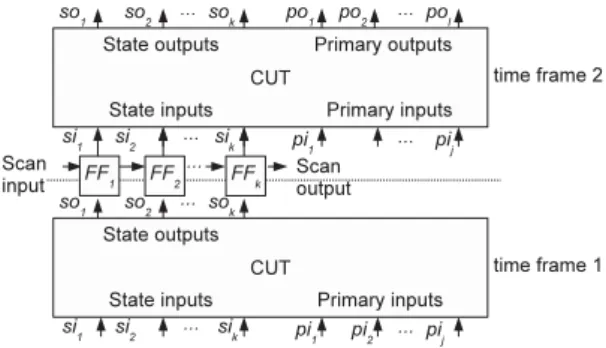
Fig. 1. Two-frame version of full scan circuit.
possibility to reduce over-testing, which is a result of scan methods that allow generation of scan patterns that are illegal during functional mode. Although this is not investigated by this work, the amount of reduction of over-testing depends on the F-scan DFT algorithm. Whenever F-scan-paths created in the circuit utilize available functional elements and paths for testing as much as possible, the circuit will generally work close to normal mode during testing. Thus, if there are lesser F-scan-paths created by adding circuitry for scan, over- testing is minimized. Other works [10], [11], [12], [13] have also proposed different techniques to identify the delay faults that are not functionally testable to reduce over-testing. These works generate test patterns for scan using the information of functionally untestable delay faults, which makes the scan tests as close to functional tests as possible.
The rest of the paper is as follows. Chapter II explains the general scan-based delay testing methods. A hybrid two- pattern test generation model for full scan is also illustrated. Our proposed method is discussed in Chapter III, including a brief background on F-scan. Experimental procedures and results are shown in Chapter IV. Finally, conclusion and future work are given in Chapter V.
II. SCAN-BASEDDELAYTESTTECHNIQUES
Using full scan for any sequential circuit allows test patterns for transition faults to be generated through combinational ATPG on a two time frame version of the circuit. Fig. 1 shows a general representation of a two-time-frame version of a full scan circuit employed on a sequential circuit [9]. The circuit has 𝑗 primary inputs, 𝑝𝑖1, 𝑝𝑖2, ...𝑝𝑖𝑗, 𝑙 primary outputs, 𝑝𝑜1, 𝑝𝑜2, ...𝑝𝑜𝑙, and 𝑘 state inputs and outputs, 𝑠𝑖1, 𝑠𝑖2, ...𝑠𝑖𝑘
and 𝑠𝑜1, 𝑠𝑜2, ...𝑠𝑜𝑘. State outputs 𝑠𝑜𝑖, where 𝑖 = 1, 2, ..., 𝑘, of the first time frame copy are connected to the state inputs 𝑠𝑖𝑖 of the second time frame copy of the circuit. This is a representation of the original circuit, wherein the state output 𝑠𝑜𝑖 and state input 𝑠𝑖𝑖 pairs are connected in a feedback loop through scan flip-flops 𝐹 𝐹𝑖. All the scan flip-flops use scan- enable to control whether to operate in normal or scan mode. The two traditional approaches to delay scan testing are skewed-load and broad-side. The timing difference for the scan enable signal between these two approaches are shown in Fig. 2. For both methods, the initialization pattern of a
Fig. 2. Delay scan-based test timing diagram.
delay test pattern pair is first loaded into all the scan flip- flops by 𝑛 consecutive scan shifts, where 𝑛 is the number of scan flip-flops in the scan chain. The launch pattern is applied after all the initialization patterns have been scanned in. Then, the response to the launch pattern is captured by the scan flip-flops at the next clock cycle after going to normal operation (at-speed). The clock speed during scan is usually slower compared to normal clock operation. Another difference between the two traditional methods is the source of the second pattern. This is described in the next subsections. A. Skewed-load
In skewed-load approach, both the initialization and launch vectors of the pattern pair are delivered through the scan cells themselves [7]. The second vector is obtained by shifting in the first pattern by one more scan flip-flop and scanning- in a new value into the scan chain input. This means that both patterns come from the scan-input. Test patterns for this approach can be generated using combinational ATPG with little modification, similar to full scan. The scan enable signal is at logic high from initialization of first patterns to the launching of second set of patterns. Then, it is switched to logic low to configure the circuit to normal operation at the next clock cycle, which is also the capture cycle. Since the clock during normal operation is faster and the clock during scan is slower, the switching of the scan enable signal needs to be fast and precise to match the timing of the circuit. Due to this, the scan enable signal should be driven by a strong clock buffer or complicated buffer tree. This requirement is very costly and it causes longer design time. Moreover, there is shift dependency in skewed-load approach, since only two possible patterns are available for the second pattern, wherein the difference is only at the first scan flip-flop that is directly connected to the scan input. If there is a transition delay fault that requires an initialization pattern with 0 at state input 𝑠𝑖𝑖−1 and a launch pattern with 1 at state input 𝑠𝑖𝑖, then this fault is shift dependency untestable, assuming that the scan chain has non-inverting outputs for all scan flip-flops. [9]
B. Broad-side
Broad-side technique is more commonly used because it solves the timing problem of scan enable in skewed-load. In this approach, the first set of patterns is scanned in to the scan chain and the second vector is derived from the combinational circuit’s response to the first vector [8]. Since the launch pattern does not come from the scan input, the scan enable
signal can be switched to logic low right after initialization. This makes broad-side cheaper to implement. Despite the advantages of broad-side in terms of cost, fault coverage achieved by broad-side is lower compared to skewed-load [8]. Since the second pattern is produced by the circuit response to the first pattern, the number of possible patterns that can be applied as launch patterns is limited, unless the circuit can switch to all 2𝑛 states, where 𝑛 is the number of flip-flops. Thus, a fault is function dependency untestable whenever a state required to activate and propagate a transition delay fault is an invalid state [9]. Additionally, the test patterns for broad- side are generated using sequential ATPG using two time- frames. This makes test generation time longer. The number of test patterns generated by broad-side is also typically larger than those generated by skewed-load [6].
With these, there is motivation to create a method that can realize the advantages of both skewed-load and broad-side, while solving their individual disadvantages as well.
C. Hybrid Model for Full Scan
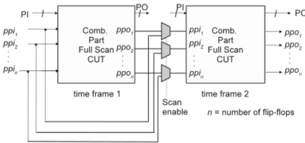
In this section, we show a hybrid model for full scan that we have used to generate delay fault test patterns for circuits. This model is called hybrid because it allows generation of test patterns for delay testing using both broad-side and skewed-load approaches. In Fig. 3, the circuit has primary inputs 𝑃 𝐼, primary outputs 𝑃 𝑂, and 𝑛 pseudo primary inputs and outputs, 𝑝𝑝𝑖1, 𝑝𝑝𝑖2, ...𝑝𝑝𝑖𝑛, and 𝑝𝑝𝑜1, 𝑝𝑝𝑜2, ...𝑝𝑝𝑜𝑛. The pseudo primary inputs and outputs represent the input and output of scan flip-flops, thus, 𝑛 is the number of scan flip- flops in the circuit. The pseudo primary inputs are connected to the pseudo primary outputs through the scan flip-flops. However, since the scan flip-flops are multiplexed, the scan enable signal controls which delay scan mode the circuit- under-test is configured. If scan enable signal is logic high during launch, the second set of patterns will come from the scan input (skewed-load). If it is logic low during launch, the second set of patterns will be the response of the combinational circuit to the first set of patterns (broad-side).
Although this approach improves the fault coverage of broad-side approach, the timing problem for the scan enable signal of skewed-load patterns is still not solved. The fault coverage of this hybrid method for ITC’99 benchmark circuits is shown in the experimental results. This ATPG model is different from what is used for the traditional skewed-load and broad-side approaches.
III. PROPOSEDHYBRIDMODEL FORDELAYFAULTATPG The proposed hybrid model for delay fault ATPG is appli- cable to F-scannable circuits. In our previous work [3], [4], F- scan proves to have higher fault coverage for any arbitrary RTL circuit compared to full scan for stuck-at faults. In this paper, we present a hybrid two-pattern test generation model for delay transition faults, wherein both skewed-load and broad- side patterns are automatically generated using combinational ATPG. This chapter gives a brief overview on F-scan and
Fig. 3. Hybrid two-pattern test generation model for full scan.
testing F-scannable circuits before discussing the proposed method for delay fault ATPG.
A. F-Scan
F-scan or functional scan is a method for scan done at RTL, in which existing functional elements and paths are maximally utilized for testing purposes [3], [4]. It primarily aims to reduce total area overhead due to test. Test application time is also kept at the minimum due to parallel and simultaneous scanning-in and -out of test vectors. Experimental results show that F-scan is superior against gate-level full scan in terms of area overhead, test application time, and fault coverage.
In gate-level full scan, flip-flops are converted to scan flip- flops by augmenting multiplexers to each flip-flop and then arranging them into scan chain(s). F-scan improves this by efficiently organizing F-scan-paths, wherein every register in the circuit is organized in an F-scan-path such that the least hardware overhead possible is achieved. Available logic in any sequential circuit is used whenever possible to create the F-scan-paths. The augmentation of the circuit to make it F-scannable happens at RTL. Thus, the circuit already includes the F-scan-paths during synthesis, wherein the circuit is optimized for size, speed, and performance once synthesized to gate-level. This allows combinational ATPG to be used for F-scannable circuits.
B. Testing F-Scannable Circuits
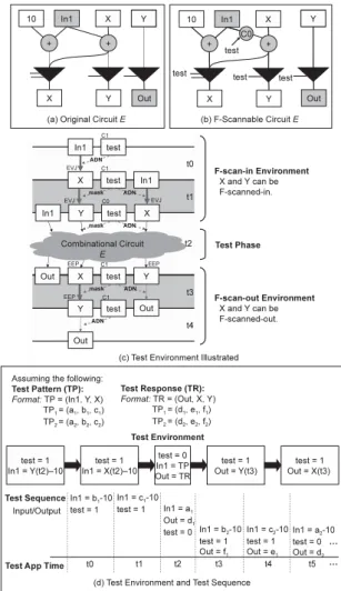
In order to test F-scannable circuits, a test environment is generated for each of the F-scan-paths in the circuit-under- test (CUT). Each F-scan-path has a schedule of scan-in and -out for every register included in the path, depending on the order of these registers along the F-scan-path. The F-scan- paths are activated using control signals (scan enable and hold, if necessary). Thus, the test environment for the entire CUT consists of the scheduled signal assignment values and output response involved to complete an F-scan cycle. Similar to full scan, an F-scan cycle consists of the F-scan-in phase, the test phase (normal mode), and the F-scan-out phase. An example of test environment generation is given in Fig. 4, which is described in more detail in our previous work [4].
The main difference of the scan operation between F-scan and full scan is that, the clock speed during scan for F-scan can be at-speed or similar to the circuit’s normal operation. Since the F-scan-paths are already integrated in the circuit during
Fig. 4. An illustration of test environment generation for F-scan by example.
synthesis, the F-scannable circuit is capable to be configured to scan mode and can operate scan functions without making the system clock slower. This advantage of F-scan makes it adaptable for testing both stuck-at faults and delay faults. Moreover, any fault model available for gate-level full scan can also be used for F-scan.
C. Hybrid Delay Test Generation Model for F-scan
The proposed hybrid two-pattern test generation model for F-scan is similar to the hybrid model for full scan presented in the previous chapter. This is shown in Fig. 5. The com- binational part of the CUT is copied to two time frames, wherein constraints regarding the F-scan-paths are included. These constraints are included in order to generate test patterns that are functionally reachable states as much as possible. The pseudo primary inputs, 𝑝𝑝𝑖1, 𝑝𝑝𝑖2, ...𝑝𝑝𝑖𝑛, and pseudo primary outputs, 𝑝𝑝𝑜1, 𝑝𝑝𝑜2, ...𝑝𝑝𝑜𝑛, where 𝑛 is equal to the number of flip-flops in the CUT, are each connected according to the F-scan-paths in both circuits. Since the F-scan-paths are created to connect registers, after synthesis to gate-level, each register is represented by a set of flip-flops of which the number depends on the bitwidth of the register. The pseudo
Fig. 5. Hybrid two-pattern test generation model for F-scan.
primary outputs 𝑝𝑝𝑜𝑖, where 𝑖 = 1, 2, ..., 𝑛, of the first time frame copy are directly connected to the pseudo primary inputs 𝑝𝑝𝑖𝑖 of the second time frame copy. Unlike in the hybrid full scan model, there are no multiplexers that connect the pseudo primary pin pairs between the two time frame copies of the CUT. This is because the F-scan-paths are already in the combinational part of the CUT. One pseudo primary input and output pair represents a single-bit F-scan-path. Thus, multiple pseudo primary inputs and outputs represent the parallel and simultaneous scan operation of F-scan.
During ATPG, the first time frame copy is constrained to a constant value at the faulty site while in the second time frame copy, stuck-at-fault is assumed. A transition between the non- faulty value to the faulty value is tested whether the fault is detected. Since this model is hybrid, the combinational ATPG tool automatically generates test patterns that can be either skewed-load or broad-side. If the F-scan enable signal of the first time frame is set by ATPG to be 1, the delay testing mode is skewed-load. If it is 0, the delay testing mode is broad-side. Since the F-scan-paths are connected in such a way that registers propagate test patterns in parallel, there is no shift dependency in between flip-flops serially. Instead, the depen- dency is parallel. During skewed-load mode, each F-scan-path receives scan input according to the bitwidth of each of the F-scan-paths. This way, there are more possible patterns avail- able for the second pattern. Moreover, since the combinational ATPG has a choice to either use broad-side or skewed-load mode to generate the test patterns, whenever a fault is hard to activate and propagate with broad-side, skewed-load approach is chosen instead.
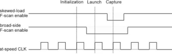
Another advantage of this hybrid model for delay fault testing, aside from the improvement of fault coverage for the traditional broad-side approach, is that the scan enable timing problem of skewed-load is solved. Since the circuit can operate at the same speed (at-speed) during normal mode and F-scan mode, there is no need for additional circuitry to control the F-scan enable at the exact fast timing. The timing diagram for both skewed-load and broad-side testing modes are shown in Fig. 6.
Regarding test generation time, improvement can be achieved when the ATPG tool used has information on handling F-scan-paths. The available ATPG tools today are already equipped to handle full scan, thus ATPG can be done more efficiently. In our experiments, we have used an available
Fig. 6. Hybrid delay F-scan-based test timing diagram.
ATPG tool to generate test patterns, which deals with the circuit as if F-scan-paths are just part of the circuit but it is not known that they are used for scan, thus increasing the test generation time. Hence, a more efficient ATPG tool for F-scan can still be done.
D. Handling Error Masking
Delay fault testing for F-scan can be applied at operational speed for both scan and normal modes, wherein the F-scan- paths may have errors that may result in error masking. From the heuristic algorithm used to create F-scan-paths described in [4], all possible errors can be propagated along F-scan-paths. Thus, we can test the F-scan-paths beforehand by scanning- in and -out test patterns without going to normal mode at operational speed and then, by checking if there are errors. If there are no errors, then error masking will never happen when testing the F-scannable circuit.
IV. EXPERIMENTALRESULTS
In our experiments, we applied both F-scan and gate- level full scan to ITC’99 Benchmark Circuits. F-scan is applied based on the heuristic algorithm described in our previous work [3], [4]. The synthesis and combinational ATPG are done using DesignCompiler and TetraMax of Synopsys, respectively. The combinational part of each benchmark is copied to two time frames and the constraints of the F- scan-paths are included. The fault list is first generated for each benchmark, then these faults are tested using the hybrid model. On the other hand, gate-level full scan chains are added to the benchmarks using DesignCompiler. Three ATPG methods were done for full scan. For skewed-load approach, TetraMax is used using the basic scan method ATPG, which is combinational. For broad-side, the fast sequential ATPG of TetraMax for two time frames is used. For the hybrid full scan method, the broad-side approach is done first, followed by the skewed-load approach, which is used to detect the faults that are not detected using broad-side. The results for fault coverage of the three full scan approaches are shown in Table I. Hybrid full scan results are compared with hybrid F-scan results in Table II. The number of test patterns for each method are given in Table III.
In Table I, the fault coverage results of the hybrid model for full scan are superior against the results of both broad-side and skewed-load approaches for all circuits. This proves that the hybrid model is the best among all methods in terms of fault coverage. Note that in these three approaches, the ATPG models are different from each other. The hybrid model for
full scan is also different compared to the hybrid model for F-scan ATPG. In Table II, we compare our method, hybrid F- scan, to the superior full scan delay fault ATPG model, hybrid full scan. For most of the circuits, except b12 and b13, the fault coverage of hybrid F-scan is better than that of hybrid full scan. There is an increase in the number of faults for most circuits due to circuit augmentation done by F-scan, all of which are made detectable in F-scan, thus increasing the fault coverage of F-scan for most cases. Nevertheless, we can also observe that the number of faults for b05 and b12 using hybrid F-scan is lower than that of hybrid full scan. This can be attributed to the effect of increased accessibility of registers and memory elements due to F-scan.
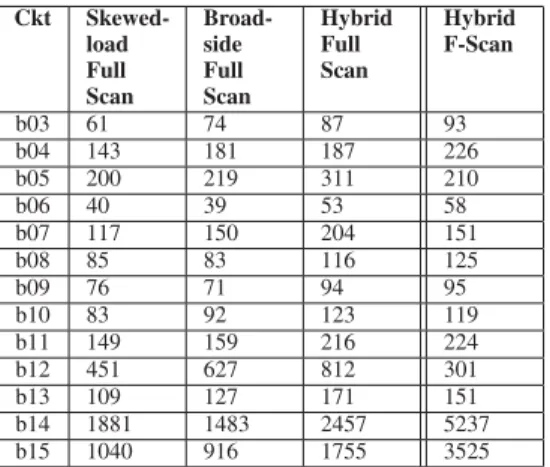
Moreover, since the ATPG tool used in this experiment does not have any information about the F-scan-paths, unlike for full scan, of which the ATPG tool already knows how to handle scan chains, the highest efficiency of ATPG may not be achieved for F-scan. The two time frame model for F-scan is time consuming because the constraint in the first time frame restricts the fault simulation. However, with the results, we have proven that it is possible to do delay fault testing on F-scannable circuits that can achieve high fault coverage. In Table III, the number of test patterns for both hybrid methods (full scan and F-scan) are relatively the same, except for b14 and b15 wherein hybrid F-scan generated more test patterns. For these circuits, a method to reduce the time for fault simulation is employed and in effect, redundant patterns still remain. Thus, if a more effective ATPG tool for F-scan is available, it is possible to reduce both the test generation time and number of test patterns produced for F-scan.
TABLE I
RESULTS FORGATE-LEVELFULLSCANDELAYFAULTATPG
Ckt Faults Skewed-load Broad-side Hybrid
FC (FE) FC (FE) FC (FE)
b03 852 82.63% (100%) 95.89% (100%) 97.77% (100%) b04 2620 83.21% (99.69%) 94.24% (99.73%) 94.66% (100%) b05 3148 87.26% (99.56%) 84.34% (99.27%) 92.57% (99.49%) b06 402 91.54% (100%) 88.81% (100%) 97.51% (100%) b07 1694 90.50% (100%) 86.48% (100%) 97.17% (100%) b08 814 85.38% (100%) 88.21% (100%) 96.44% (100%) b09 784 96.81% (100%) 96.17% (100%) 99.62% (100%) b10 858 92.89% (100%) 89.51% (100%) 97.20% (100%) b11 2072 86.20% (100%) 85.23% (100%) 95.22% (100%) b12 6050 94.21% (100%) 90.83% (100%) 98.60% (100%) b13 1756 92.14% (100%) 88.44% (100%) 97.10% (100%) b14 36376 96.71% (97.20%) 83.28% (84.66%) 98.32% (99.12%) b15 23202 79.47% (98.22%) 58.19% (60.54%) 93.40% (99.35%)
V. CONCLUSIONS ANDFUTUREWORK
In this work, we have presented a hybrid two-pattern test generation model for F-scan for delay fault testing. Since the F-scan-paths are designed such that they utilize the available functional logic and paths to connect all registers, they are usable to test any arbitrary RTL circuit with any fault model available for full scan. We have proven the effectiveness of our hybrid model used for F-scan in terms of fault coverage against the traditional delay testing techniques for full scan,
TABLE II
FAULTCOVERAGERESULTS FORHYBRIDFULLSCAN ANDHYBRID F-SCAN
Ckt Hybrid Full Scan Hybrid F-Scan
Faults FC (FE) Faults FC (FE)
b03 852 97.77% (100%) 1074 99.35% (100%) b04 2620 94.66% (100%) 3116 96.37% (100%) b05 3148 92.57% (99.49%) 2668 93.07% (100%) b06 402 97.51% (100%) 566 98.23% (100%) b07 1694 97.17% (100%) 2142 96.69% (100%) b08 814 96.44% (100%) 1046 99.81% (100%) b09 784 99.62% (100%) 1080 98.52% (100%) b10 858 97.20% (100%) 1122 99.91% (100%) b11 2072 95.22% (100%) 2464 99.03% (100%) b12 6050 98.60% (100%) 3296 95.45% (100%) b13 1756 97.10% (100%) 2214 96.03% (100%) b14 36376 98.32% (99.12%) 41690 99.29% (99.94%) b15 23202 93.40% (99.35%) 29464 95.71% (99.95%)
TABLE III
COMPARISON OF THENUMBER OFTESTPATTERNSAMONGDIFFERENT DELAYFAULTATPG TECHNIQUES
Ckt Skewed- load Full Scan
Broad- side Full Scan
Hybrid Full Scan
Hybrid F-Scan
b03 61 74 87 93
b04 143 181 187 226
b05 200 219 311 210
b06 40 39 53 58
b07 117 150 204 151
b08 85 83 116 125
b09 76 71 94 95
b10 83 92 123 119
b11 149 159 216 224
b12 451 627 812 301
b13 109 127 171 151
b14 1881 1483 2457 5237
b15 1040 916 1755 3525
skewed-load and broad-side. We have also compared our work with a similar hybrid model applied to full scan. F-scan has high fault coverage for delay faults on all benchmarks using the hybrid model. Also, the hybrid model can be configured to generate broad-side test patterns only, wherein there is a possibility of reduction of over-testing, since the launch test patterns will come from the functional circuit only.
The hybrid model for F-scan solved the timing problems of full-scan skewed-load because F-scan can operate at operation speed during scan and normal modes. This means that there is no need to meet the strict timing requirement for the scan enable signal during skewed-load approach. Moreover, since both skewed-load and broad-side are integrated in one delay test technique for F-scan, the concern on shift dependency and function dependency with regards to the flexibility of the patterns produced during ATPG is given solution.
An important issue to tackle next is the improvement of test generation since using the two time frame stuck-at ATPG model takes a lot of effort and time. Also, another concern is the power consumption during test using the hybrid F- scan delay scan testing. In most cases, power consumption
during test mode is higher than during normal operation [15]. Moreover, the switching activity of the test patterns could affect their capability to detect faults, moreso since the circuit operates at high speed even during testing. Thus, it is necessary to determine the optimum switching activity of the test patterns for F-scan that can reduce power consumption and error due to fast switching as much as possible. Moreover, over- testing reduction can be focused by the F-scan heuristic and experiments can be done to prove its effectiveness.
ACKNOWLEDGMENT
This work was supported in part by Japan Society for Promotion of Science (JSPS) under Grants-in-Aid for Scien- tific Research (B) (No. 20300018) and for Young Scientists (B) (No. 22700054). The authors thank Prof. Michiko Inoue, Prof. Tomokazu Yoneda, and the members of the Computer Design and Test Laboratory in Nara Institute of Science and Technology for their valuable comments and suggestions during discussions regarding this work.
REFERENCES
[1] H. Fujiwara, Logic Testing and Design for Testability, Cambridge, MA: MIT Press, 1985.
[2] A. Krstic and K-T. Cheng, Delay Fault Testing for VLSI Circuits, Kluwer Academic Publishers, 1998.
[3] M. E. J. Obien and H. Fujiwara, “F-Scan: An approach to functional RTL scan for assignment decision diagrams,” Proc. IEEE 8th Int. Conf. on ASIC, pp. 589-562, Oct. 2009.
[4] M. E. J. Obien and H. Fujiwara, “A DFT method for functional scan at RTL,” Proc. 10th IEEE Workshop on RTL and High Level Testing, pp. 6-15, Nov. 2009.
[5] D. Belete, A. Razdan, W. Schwarz, R. Raina, C. Hawkins, and J. More- head, “Use of DFT techniques in speed grading a 1GHz+microprocessor,” Proc. IEEE International Test Conference, pp. 1111-1119, 2002. [6] J. Saxena, K. M. Butler, J. Gatt, R. R. S. P. Kumar, S. Basu, D. J. Camp-
bell, and J. Berech, “Scan-based transition fault testing - implementation and low cost test challenges,” Proc. IEEE International Test Conference, pp. 1120-1129, 2002.
[7] J. Savir and S. Patil, “Scan-based transition test,” IEEE Trans. on Computer Aided Design of Integrated Circuits and Systems, Vol. 12(8), August 1993.
[8] J. Savir and S. Patil, “Broad-side delay test,” IEEE Trans. on Computer Aided Design of Integrated Circuits and Systems, Vol. 13(8), August 1994.
[9] S. Wang, X. Liu, and S. Chakradhar, “Hybrid delay scan: a low hardware overhead scan-based delay test technique for high fault coverage and compact test sets,” Proc. Design, Automation and Test in Europe Conf., pp. 1296-1301, 2004.
[10] Y-C. Lin, F. Lu, K. Yang, and K-T. Cheng, “Constraint extraction for pseudo-functional scan-based delay testing,” Proc. IEEE ASP-DAC, pp. 166-171, 2005.
[11] Z. Zhang, S.M. Reddy, I. Pomeranz, “On generating pseudo-functional delay fault tests for scan designs,” Proc. IEEE International Symposium on Defect and Fault Tolerance in VLSI Systems, pp. 398-405, 2005. [12] F. Yuan and Q. Xu, “On systematic illegal state identification for pseudo-
functional testing,” Proc. 46th Annual Design Automation Conference, pp. 702-707, 2009.
[13] I. Pomeranz, “On the generation of scan-based test sets with reachable states for testing under functional operations conditions,” Proc. IEEE Design Automation Conference, pp. 928-933, 2004.
[14] V. Chaiyakul, D. D. Gajski, and L. Ramachandran, “High-level trans- formations for minimizing syntatic variances,” Proc. Des. Autom. Conf., pp. 413-418, 1993.
[15] J. Saxena, K.M. Butler, and L. Whetsel, “An analysis of power reduction techniques in scan testing,” Proc. International Test Conf., pp. 670-677, 2001.