Test Generation and DFT Based on Partial Thru Testability
Nobuya Oka
†, Chia Yee Ooi
‡, Hideyuki Ichihara
†, Tomoo Inoue
†, and Hideo Fujiwara
∗†Graduate School of Information Sciences, Hiroshima City University 3-4-1, Ozuka-higashi, Asaminami-ku, Hiroshima, 731-3194 Japan
‡Faculty of Electrical Engineering, Universiti Teknologi Malaysia, 81310 UTM Skudai Johor MALAYSIA
∗Graduate School of Information Science, Nara Institute of Science and Technology, Kansai Science City 630-0192. Japan TEL/FAX: +81-82-830-1569
[email protected],{ichihara, tomoo}@hiroshima-cu.ac.jp, [email protected], [email protected]
Abstract
Acyclically testable sequential circuits are known to be practically testable, and a sufficient condition for acyclically testability has been proposed. A sequential circuit that sat- isfies the sufficient condition is here called full thru testable. This paper propose a new class of acyclically sequential cir- cuits, called partial thru testable. The sufficient condition for our partial thru testability is easier than that for full thru one, We present a DFT and test generation method based on the proposed partial thru testability. Experimental results show that the DFT and test generation based on partial thru testability is practically effective in reducing area overhead and test application time compared with those based on full thru testability.
Key words : acyclical testability , partial thru testability, design for testability, time expansion model , combinational test generation algorithm.
1 Introduction
The test generation problem even for combinational cir- cuits is shown to be NP-complete [1], but empirical observa- tions tell us that the test generation complexity of practically encountered combinational circuits seems to be polynomial [2]. On the other hand, the problem of test generation for se- quential circuits is hard to be solved in practicable time, and hence in many cases, the problem is converted into that for combinational circuits by full scan design.
Some sequential circuits, however, are practically tractable in the same way as combinational ones. Ooi et al. introduced that some sequential circuits can be classified by denoting τ=Θ(nr) (n is the size of the combinational cir- cuit, r is some constant larger than 2) as the test genera- tion complexity of combinational circuits [3]. For example, the test generation complexity for the sequential circuits that have balanced structure, strongly balanced structure or inter- nally balanced structure is equivalent to combinational test generation complexity[4, 5, 6]. The test generation problem for general acyclic sequential circuits is comparatively easily [7] but more hardly testable than that for combinational cir- cuits. In addition, the authors introduced a wider class called acyclically testable sequential circuits whose test generation complexity is the same as acyclic sequential circuits. Note
that this class is larger than that of acyclic sequential cir- cuits but its test generation complexity is equivalent to that of the acyclic sequential circuits [8]. They defined a thru tree whose root is a primary output, its leaves are primary inputs and each of its edges represents a thru function, and proposed a sufficient condition for acyclical testability based on the thru trees.
In this paper, we propose a new class of acyclically testable sequential circuits. Defining pairs of justification and propagation thru trees instead of the thru trees defined in [8], we show a sufficient condition for acyclical testabil- ity with the thru tree pairs, and call the circuits that satisfy the condition partial thru testable. In contrast, we call se- quential circuits that satisfy the condition presented in [8] full thru testable. We also present a design-for-testabililty (DFT) method for making a given sequential circuit partial thru testable with small hardware overhead. The proposed class of partial thru testable sequential circuits is larger than that of full thru testable ones, and therefore the DFT over- head based on partial thru testability must be smaller than that based on full thru testability. Experimental results show that, compared with the DFT method based on full thru testa- bility, the proposed DFT method based on partial thru testa- bility can reduce not only hardware overhead, but also test application time.
2 Background and Motivation
2.1 BackgroundLet us consider a sequential circuit S1, having feedback cycles, as shown in Fig. 1. A sequential circuit is composed of combinational logic blocks (CLBs), registers and connec- tions between CLBs and registers. Some registers may have a hold mode1. All CLBs except C5 and C6 have thru func- tions – a thru in a CLB transfers an input data to an output of the CLB independet of the CLB logic.
Sequential circuit S1in Fig. 1 satisfies the sufficient con- dition for acyclical testability presented in [8]. Even though an acyclically testable sequential circuits is cyclic, test gen- eration complexity of the circuits is equivalent to that of the acyclic sequential circuits. An acyclically testable circuit has
1A register with a hold mode can retain its content, and it is assumed to be controlled independent of the circuit.
2009 IEEE European Test Symposium, poster session, May 2009.
t6 PI2
C1 PI1 t1
R1
R4 C2 R2
C3 R3
● C4
PO1 t2
C6
C7 R5
t3 R7 PI3
C9
R8 R9
C8
t4 ●
●
● PO2
● ● t5
● C5
C10 C11
R6
t7 t8
t9
Figure 1. Sequential circuit S1.
CLB
(a)simple thru function
CLB
(b)merge thru function t1
t2
t3
t3 m1
m2 m3
m6 m7 m8 m4=m1 m5=m2
m9=m6+m7 m10 a
b c
f g h d e
i j
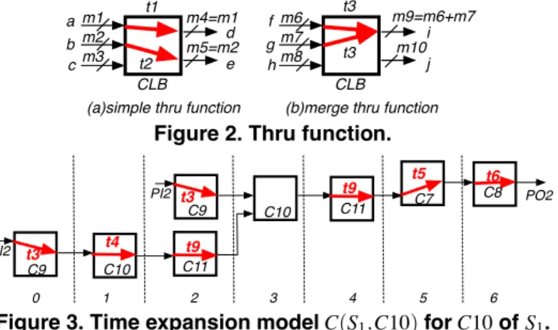
Figure 2. Thru function.
C10 C11 t4 C9
PI2 t3
C9 C10 PI2 t3
C11
t6
C7 C8 PO2
t5
t9
t9
6 5 4 3
2 1
0
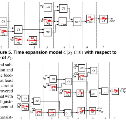
Figure 3. Time expansion model C(S1,C10) for C10 of S1.
thru trees such that the root is a primary output, the inter- nal nodes are registers, the leaves are primary inputs and the edges represent thru functions. Any register on a thru tree can be justified from primary inputs, and can be observed at the primary output with thru functions. For example, the path (PI1,R1,R2,R3,PO1) in S1corresponds to a thru tree. Accordingly, R1, R2 and R3 can be justified from PI1, and can be observed at PO1 with thru functions t1, t7, t8 and t2. Test generation for acyclically testable circuits can be per- fomed with combinational ATPG, in a similar way of that for acyclic sequential circuits. For example, consider test gen- eration for CLB C10 of S1. Test generation for acyclically testable sequential circuits can be perforemed on a time ex- pansion model (TEM) as shown in Fig. 5. A TEM consists of CLBs and their connections with information about the time at which each register loads a new data or holds its content. Though S1 has two cycles consisting of registers {R1,R2,R3} and {R8,R9}, these registers can be justified from primary inputs, and can be observed at primary outputs owing to thru trees. Therefore, R9 and R7 connecting to the inputs of CLB C10 can be justified with thru functions t3, t4 and t9, and R8 that connecting to the output of CLB C10 can be observed with thru functions t5, t6 and t9. A test pattern generated on TEM C(S1,C10) can be transformed into a test sequence for CLB C10 in sequential circuit S1. For other CLBs, test generation can be perfomed with TEMs constructed in a similar way.
2.2 Motivation
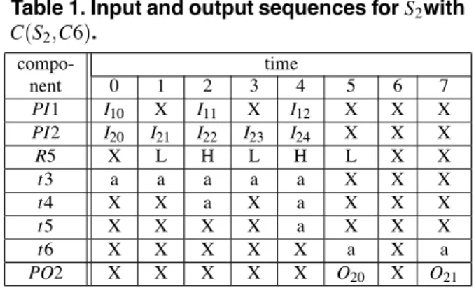
Let us consider a sequential circuit S2 in Fig. 4. CLBs C2, C3 and C11 have no thrus, and hence S2 has no thru tree unlike S1. Accordingly, S2is not accyclically testable. However, we can obtain a TEM for any CLB. For example, a TEM with respect to CLB C10 in S2is shown in Fig. 5. This example implies that acyclically testable sequential circuits do not necessary require full thru trees whose root and leaves are a primary output and primary inputs, respectively. Note that in S2, any thru tree either begins at primary inputs (or leaves) or ends at a primary output (or a root). Accordingly, we call such a sequential circuit as S2partial thru testable. In contrast, a circuit satisfying the sufficient condition in [8]
is called full thru testable. In the next section, we discuss a sufficient definition for partial thru testability.
3 Partial thru testability
We propose partial thru testability as an extended class of full thru testable sequential circuits. In addition, we propose a test generation procedure for partial thru testable sequential circuits. Due to space limitation, we outline the definition and the proof of testability of the proposed circuits.
Here, we consider two types of thru functions as shown in Fig. 2. One is simple thru: it transfers the data of an input of the CLB to an output independent of other inputs. All the thru functions used in the circuit of Fig. 1 are simple thrus. The other is merge thru: it binds the data of a certain number of inputs and transfers them to an output without modification. When an input value of a CLB with a thru function tiis transferred to the output by the function ti, thru tiis said to be activated.
3.1 Partial thru testable sequential circuits
A sufficient condition for partial thru testability is based on two thru trees: justification and propagation thru trees in- stead of the thru trees defined in [8].
A justification thru tree TJis a tree such that any leaf cor- responds to a primary input and any connection has a thru function. A propagation thru tree TPis a tree such that the root corresponds to a primary output and any connection has a thru function. When all thru functions in a justification thru tree TJ is activated, any register in the tree can be justified from primary inputs. When all thru functions in a propaga- tion thru tree TPis activated, any register in the tree can be observed from a primary output.
(Example1) The sequential circuit shown in Fig. 4 has jus- tification thru trees T1Jand T2J, and propagation thru trees T1P and T2P. Justification thru tree T1Jhas a leaf PI1 with a node R1 by a thru function t1. Justification thru tree T2Jhas a leaf PI2 with nodes R8 and R7 by thru functions t3 and t4. Prop- agation thru tree T1Phas a root PO1 with a node R3 by a thru function t2. Propagation thru tree T2P has a root PO2 with nodes R9 and R6 by thru functions t5 and t6.
The condition for the justificatoin and propagation thru
t6 PI2
C1 t1 PI1
R1
R4 C2
R2 C3
R3
● C4
PO1 t2
C6
C7 R5
t3 R7
PI3 C9 R9
R8
C8
t4 ●
●
● PO2
● ● t5
● C5
C10 C11
R6
Figure 4. Sequential circuit S2.
C11
C10 t4 C9 PI2 t3
C6 C5
C9 t3 PI1
PI2
C9 C10 PI2 t3
C11 C5 C6
PI1
t6
C7 C8 PO2
t5
6 7
5 4 3
2 1
0
●
Figure 5. Time expansion model C(S2,C10) with respect to C10 of S2.
trees for partial thru testable circuits consists of several sub- conditions. One of the subconditions is that justification and propagation thru trees can break (or go through) all the feed- back loops, respectively. If this condition is satisfied, at least one register on included by each cycle in a sequential circiut can be justified or propagated. Note that registers covered with justification thru trees is not always identical to that with propagation thru trees. If same registers is coverd with justi- fication thru trees and propagation thru trees in a sequential circuit, the sequential circuit is full thru testable.
(Example2) Sequential circuit S2 has two cycles consist- ing of registers{R1,R2,R3} and {R8,R9}. Justification thru trees T1J and T2Jcover registers R1 and R8, and propagation thru trees T1Pand T2Pcover registers R3 and R9. Therefore, we can justify (resp. observe) registers on every cycle with thru functions.
In addition to the definition for partial thru trees, we need consider several conditions for a use of thru functions. (Example3) Consider a pair of paths p= (PI1,R1,R2) and q= (PI1,R4,R2) in S2. Note that the connection of PI1 and R1 has thru function t1. Suppose that R1 and R4 should be justified when R2 is justified. Because R1 is included in the justification thru tree T1J, any value can be propagated to R1 with thru function t1. On the other hand, another value on PI1 is required to justify R4. Accordingly, the requirements on PI1 conflict, and any particular values can not be justified to R1. In this case, the conflict can be avoided with a hold function of a register. If R1 or R4 have a hold function, R1 and R4 can be justified.
The condition for hold registers in partial thru testable cir- cuits is the same as that in full thru testable circuits. In the case of S2, if registers R1 or R4 and R5 or R8 have hold func- tion, the condition for hold registers in partial thru testable circuits is satisfied.
According to the definition of partial thru trees, a full thru tree is both a justification thru tree and a propagation thru tree. Thus, the class of partial thru testable sequential circuits includes that of full thru testable sequential circuits.
3.2 Testability of partial thru testable sequential circuits
In this section, we explain that the test sequence of a par- tial thru testable sequential circuit is obtained with the test
I23 I24 I12
PI2
I20 I10
PI2
I21
PI2 t6
C6
t3 C7 C9
t4 t5 C8
C5
C10 C11
t3 C9
t6 C6
t3 C7 C9
t4 C8
PO2 C5
C10 C11
t3 C9
C6 C5
I22 I11
O21
O20
0 1 2 3 4 5 6 7
PI1
PI1
PI2
PI1
PI2
t3 C9
PO2
Figure 6. Time expansion model C(S2,C6) with respect to C6 of S2.
patterns of time expansion models.
3.2.1 Time expansion model
We define time expansion model (TEM) with respect to CLB of S as a test generation model for partial thru testable se- quential circuits S. A TEM consists of CLBs and their con- nections, and represents the time when the output of each CLB is determined by other CLBs. The number located at the down of each column denotes the relative time difference of CLBs, primary inputs and primary outputs. Here, we call the number cycle label. For example, let us consider a CLB C11 with cycle label 3 in Fig. 6. If an input pattern I10 is applied to a primary input PI01with cycle label 0, the CLB C11 is affected from the pattern after three cycles. Note that a TEM has no registers and thereby is a combinational circuit. The structure of TEM with respect to Ciof S satisfies the following conditions.
• There exists a CLB in S corresponding to any CLB in the TEM.
• For any connection between two CLBs in TEM, the dif- ference of cycle label is the number of load registers or several hold registers.
• If a thru function of a CLB in the TEM is activated, the CLB has successors corresponding to inputs of the thru function. The other CLBs has all successors corre- sponding to inputs of the CLB in S.
• A set of propagation paths for CLB Ciin S that has all successors corresponding to inputs of the CLB in S must be guaranteed in the TEM. Here, a propagation path is from an output of Cito a register in a propagation thru tree or a primary output.
• The cycle label for each CLB is unique, i.e., there is at least one CLB with an identical cycle label.
• The same connection doesn’t exist at the same cycle la- bel.
(Example4) Let us consider a TEM with respect to C6 of S2C(S2,C6) shown in Fig. 6. S2has two propagation paths of C6. One is a path from output register R5 of C6 to input register R6 of C8, it is called p1. The other is a path from R5 to input register R9 of C7, it is called p2. In TEM C(S2,C6), there is the path p1from C6 with cycle label 5, and the path p2from C6 with cycle label 1. In C7 with cycle label 4, thru function t5 is activated for propagation path p2. Therefore, the only input of C4 is an output of C11 . In C7 with cycle label 6, thru function t5 isn’t activated for propagation path p1. Therefore, the inputs of C7 are outputs of C6 and C11. 3.3 Testability of partial thru testable sequential
circuits
Here we consider the relationship between input/output sequences of a partial thru testable sequential circuit and in- put/output patterns of its TEM. We can obtain test patterns by applying a combinational ATPG to the TEM derived from a given partial thru testable sequential circuit because a TEM is combinational circuit. The input/output patterns for a TEM can be transformed to input/output sequences and control se- quences of registers for the sequential circuit with the struc- ture of TEM.
(Example5) Consider a TEM with respect to C6 of S2
C(S2,C6) of a sequential circuit S2 shown in Fig. 4. Sup- pose an input-pattern(PI10,PI11,PI12,PI20,PI21,PI22,
PI23,PI24) = (I10,I11,I20, I21, I22, I23,PI23,I24) and an output-pattern is(PO1,PO2) = (O20,O21). In control input sequences for hold register, H describes hold mode and L describes load mode. Table. 1 shows input and output se- quences for S2with the information of the TEM. Here, X denotes a don’t-care value.
In addition, a TEM with respect to a CLB B for a partial thru testable sequential circuit S can be obtained from con- trol input sequences for the S and input/output patters for the TEM can be obtained from input/output sequence for the S. From the above discussion, we can derive test sequences for the S by obtaining test patterns for the faults in TEM Ci. 3.4 Test generation procedure
The test sequences of a partial thru testable sequential cir- cuit for each stuck-at fault can be obtained by the following procedure. Let BSand F be a set of CLBs and a set of faults in a target sequential circuit S, respectively. First, select a
Table 1. Input and output sequences for S2with C(S2,C6).
compo- time
nent 0 1 2 3 4 5 6 7
PI1 I10 X I11 X I12 X X X
PI2 I20 I21 I22 I23 I24 X X X
R5 X L H L H L X X
t3 a a a a a X X X
t4 X X a X a X X X
t5 X X X X a X X X
t6 X X X X X a X a
PO2 X X X X X O20 X O21
target CLB B in BS. If faults in B are included in F, performs the following procedure.
1. Generates TEM for B of a sequential circuit S.
2. For the generated TEM, derive the fault list FL which is faults in CLBs that are not activated thru functions. 3. Apply combinational ATPG for multiple fault model to
the TEM with FL.
4. Derive the test sequence for FL from the test patterns obtained for the TEM with the transformation that is denoted in example 4.
5. Remove FL and faults that is evaluated detectable with fault simulation from F.
6. If F ̸=φ, the above procedure is repeated to detect re- maining faults.
4 DFT Method
Let us consider a DFT method to modify a given sequen- tial circuit into a partial thru testable sequential circuit. The DFT method is to add thru functions to CLBs and hold func- tions to registers. We introduce a heuristic algorithm for cre- ating partial thru trees with small hardware overhead. Here, for the sake of simplicity, we assume that the bit-width of any register in a sequential circuit is identical. The following pro- cedure shows the brief of the proposed heuristic algorithm. Due to space limitation, we show the algorithm for creating justification thru trees.
1. Calculate the minimum number of thru functions re- quired for converting a path from a primary input to the register into a path whose all edges have thru functions. We consider the number to be a heuristic measure for creating justification thru trees.
2. Check the existence of a feedback component, which represents registers on feedback loops in the target se- quential circiuit. If there remains a feedback compo- nent, this algorithm is repeated.
3. Select a register that becomes the root of a justification thru tree. The selected register is included in the reg- ister set of the feedback components. The priority of the selection is the order as follows: (1) register r is in-
C1 R1
PI1
PI0 C3
R3 C5
R5
● PI3 C2
PI2
C4
● R4
●
● C7
PO0
C6
C8 R2
R6
R7
●PO1
Figure 7. Sequential circuit S3.
C1 R1 PI1
PI0
C3 R3
C5 R5
●
C7 PO0
C6
C8
R6
R7
●PO1 R4
Figure 8. Sequential circuit S′3.
R1 C3
R3 C5
R5
●
C7 PO0 C8
R6
R7 PO1
Figure 9. Sequential circuit S′′3.
C1 R1 PI1
PI0
C3 R3
C5 R5
● C2
PI3 PI2
C4
● R4
●
● C7
PO0
C6
C8 R2
R6
R7
●PO1 t1
t3
t2
t4
t5
t6
Figure 10. Result of applying the DFT method to S3.
cluded by a self-loop, (2) r has the minimum number of the heuristic measure, (3) r is included by the largest component.
4. Search a path for creating a justification thru tree. Note that the searched path becomes a justification thru tree by adding thru functions to arcs on the path. The path search is performed a trace from register r to a primary input. On the trace, when a register has more than two inputs from registers, the registers with the minimum number of the heuristic measure of all is added the path. 5. Update the information about feedback components in
the target sequential circuit.
(Example6) Let us consider an example of the proposed DFT algorithm for justification thru trees with a sequen- tial circuit S3 shown in Fig.7. This circuit has three feed- back components: {R1,R3,R5},{R2,R4},{R6,R7}. In Fig. 7, register R4 is selected by operation 2 because R4 is in- cluded by self-loop. Next, a path {(PI2,R2,R4)} is dis- covered according to operation 3, and the path becomes a justification thru tree. After that, S3shown in Fig. 7 is up- dated to S3′ shown in Fig. 8 with the information of the new justification thru tree. Then S3′ has two components: {R1,R3,R5},{R6,R7}. According to the algorithm, register R1 and R6 are selected, path{(PI1,R1)} and {(R4,R6)} be- comes a new justification thru tree and S3′ shown in Fig. 8 is updated to S′′3shown in Fig. 9. Finally, because S′′3does not have a feedback component, the algorithm terminates. As a result, two justification thru trees is created. One of the tree is that the leaf is PI1, the node is R1 and an arc has a thru function t1 Another of the tree is that the leaf is PI2, the nodes are R2,R4 and connections have thru functions t3 and t4.
For the case of creating propagation thru trees, the cal- culational method of the heuristic estimation and the path
search are modified. By applying the algorithms for creating two partial thru trees, we can determine that six thru func- tions is added shown in Fig. 10.
5 Experimental Results
We show the effectiveness of the proposed class by our ex- periments, using Dell PowerEdge 2950 (Red Hat Linux v.5, CPU 2.33Ghz Quad, Memory 4GB) . Table 2 shows name of circuit, number of FFs, circuit area, area overhead, num- ber of test patterns, test application cycle and test generation time.
For five sequential circuits shown in Table 2, we at- tempted three types of DFTs: full-scan design (FS), full thru testable design (FT) and partial thru testable design (PT). In FS, all registers are replaced with scaned-FFs. In FT and PT, some thru functions are added to CLBs with a heuristic algo- rithm introduced Section 4. After the DFTs, we performed the procedure described in Section 3.4. Note that, in FS, a TEM for a CLB corresponds to the CLB. Target faults of each circuit were faults in each CLB and wires between ele- ments in the circuits. In our experiments, we converted such a multiple fault into a single fault by the method of [9] and employ TetraMax (Synopsys, Inc.), which is a combinational TPG for single stuck-at faults. The circuit area was estimated provided that the area size of an inverter is one. We achieved 100% fault efficiency for all the circuits with three DFTs.
Column area overhead shows the difference of the cir- cuit size before and after the DFTs. The test application cycle shown in the seventh column for FS is calculated by(number o f test patterns) × ((number o f FFs) + 1) + (number o f FFs), and that for AT and EAT is calculated by (number o f test patterns) × (length o f T EM).
From Table 2, we can see the followings. The area over- head for FT and PT is smaller than that for FS. Moreover, our method, PT, needs smaller area overhead than FT. This is because the number of thru functions required by PT is
Table 2. Experimental Results.
circuit #FFs circuit DFT area #test test application test generation
area overhead patterns time (cycle) time[s]
FS 280 56 2336 0.00
ex1 40 3065 FT 73 56 336 0.05
PT 49 58 348 0.13
FS 672 41 4073 0.02
ex2 96 4949 FT 96 56 280 0.04
PT 48 48 288 0.35
FS 336 71 3527 0.11
lwf 48 5262 FT 145 82 492 0.30
PT 97 71 426 1.05
FS 616 74 6674 0.04
trap 88 5369 FT 75 90 720 0.11
PT 50 89 712 0.26
FS 672 84 8244 111.32
diff 96 6687 FT 194 88 880 136.63
PT 48 59 531 798.92
less than that of FT.
The test application cycle for FT and PT is smaller than that for FS since FT and PT do not need scan operation. For lwf, trap and diff, the test application cycle for PT can be small as compared with FT. The reason is that the number of test patterns of three circuits can be small. For ex2, although the number of test patterns for PT is smaller than FT, the test application cycle for PT is not. This is because the sum of the length of TEMs for PT is greater than that for FT.
Three DFTs are comparable in the number of test patterns. For ex2, lwf, trap and diff, the number of test patterns of PT can be small as compared with FT. The reason is that TEMs of PT is often implemented justification and propagation of values without using thru functions. Because the number of thru functions required for PT is less than that of FT. There- fore, the one test pattern of PT can find many faults compared with that of FT.
The test generation time for PT increased compared with that for FS and FT. The reason is that the size of TEMs for PT is larger than that for FS and FT. Because the logic of CLBs instead of thru functions is used for justification and propagation as frequently as possible in PT. However, since a TEM is a combinational circuit, we can achieve complete fault efficiency with practical time.
6 Conclusion
In this paper, we proposed the partial thru testable se- quential circuits. In the new class, we defined justification and propagation thru trees instead of the thru trees presented in [8] and proposed a sufficient condition of the class. In addition, we propose a test generation procedure and DFT method for the new class. Experimental results show that the DFT and test generation based on partial thru testability is practically effective in reducing area overhead and test appli- cation time compared with those based on fullthru testability.
Our future work includes investigating further extension of testable classes of sequential circuits.
Acknowledgments
The authors would like to thank the members of Com- puter Design and Test Laboratory, Nara Institute of Science and Technology, Japan and Dr. Yuki Yoshikawa and other members of Computer Design Laboratory, Hiroshima City University, Japan for their valuable comments.
References
[1] H. Fujiwara, Logic Testing and Design for Testability, MIT Press, 1985.
[2] M.R. Prasad, P. Chong, and K. Keutzer,“ Why is ATPG easy? ”Proc. 36th DAC, pp. 22-28, June 1999.
[3] C. Y. Ooi, T. Clouqueur and H. Fujiwara, ”Classification of sequential circuits based onτknotation and its applications”, IEICE Trans. on Info. and syst., pp.2738-2747, Dec. 2005.
[4] R. Gupta and M. A. Breuer,“ The BALLAST methodology for struc- tured partial scan design,” IEEE Trans. Comput., vol. 39, no. 4, pp. 538-544, April 1990.
[5] A. Balakrishnan and S. T. Chakradhar, ”Sequential circuits with com- binational test generation complexity,” in Proc. IEEE Int. Conf. VLSI Des., pp. 111-117, Jan. 1996.
[6] H. Fujiwara,“ A new class of sequential circuits with combinational test generation complexity,” IEEE Trans. Comput., vol. 49, no. 9, pp. 895-905, Sept. 2000.
[7] T. Inoue, D. K. Das, C. Sano, T. Mihara, and H. Fujiwara, ”Test gener- ation for acyclic sequential circuits with hold registers,” Proc. International Conf. on Computer Aided Design, pp. 550-556, Nov. 2000.
[8] C. Y. Ooi and H. Fujiwara, ”A new class of sequential circuits with acyclic test generation complexity,” IEEE Proc. ICCD, pp.425-431, Oct. 2006.
[9] H. Ichihara, and T. Inoue, ”A method of test generation for acyclic sequential circuits using single stuck-at fault combinational ATPG,” IEICE Trans. Fundamentals, Vol. E86-A, No. 12, pp. 3072-3078, Dec. 2003.