Optimization of NoC Wrapper Design Under Bandwidth and Test Time Constraints
Fawnizu Azmadi Hussin, Tomokazu Yoneda, and Hideo Fujiwara
Graduate School of Information Science, Nara Institute of Science and Technology Kansai Science City, 630-0192, Japan
fawniz-h, yoneda, fujiwara @is.naist.jp
Abstract
In this paper, two wrapper designs are proposed for core- based test application based on Networks-on-Chip (NoC) reuse. It will be shown that the previously proposed NoC wrapper does not efficiently utilize the NoC bandwidth, which may result in poor test schedules. Our wrappers (Type 1 and Type 2) complement each other to overcome this inefficiency while minimizing the overhead. The Type 2 wrapper uses larger area overhead to increase bandwidth efficiency, while the Type 1 takes advantage of some special configurations which may not require a complex and high-cost wrapper. Two wrapper optimization algorithms are applied to both wrapper designs under channel bandwidth and test time constraints, resulting in very little or no increase in the test application time compared to conventional TAM approaches.
1. Introduction
The NoC [1] provides abundant communication resources, which makes the traditional approach of adding extraneous Test Access Mechanism (TAM) [2, 3] overkill. Several re- search groups have published works on NoC test scheduling [4, 5, 6] utilizing the NoC as the test data transportation path from external testers to the CUTs. Test scheduling for the NoC router [6, 7] and crosstalk test of the interconnects [8] have also been discussed. In these approaches, each CUT is wrapped by an IEEE 1500 [9] compatible wrapper in order to provide isolation and access during the test application.
Many NoC architectures have been proposed such as SPIN [10], Æthereal [11, 12], SoCIN [13], NOSTRUM [14], QNoC [15], and HERMES [16]; all are based on a synchronous com- munication between nodes. Several other types of NoCs such as CHAIN [17], NEXUS [18], and ANoC [19] are based on Globally Asynchronous Locally Synchronous (GALS) com- munication. The copious NoC architectures highlight the growing interest in NoC as a next generation SoC intercon- nect.
With regard to the NoC’s Design-for-Testability (DFT), the authors in [20] presented an architecture called ANoC-TEST, which targets the Asynchronous Networks-on-Chip (ANoC) [19]. In [21], the proposed NoC wrapper takes advantage of
the guaranteed bandwidth and latency provided by the NoC to ensure test data integrity. Their experimental results showed that in terms of core test time, the proposed NoC wrapper is comparable to the TAM-based IEEE 1500 wrapper, and NoC- reuse [4, 5, 6] capable. However, due to the constraint of the parallel-serial conversion at the input port, the proposed wrapper requires much higher guaranteed bandwidth on the NoC than the actual rate of the test data loaded into the test wrapper. This is further explained in Sect. 4.2
In this paper, we are proposing two types of NoC wrappers based on the guaranteed bandwidth and latency. The wrappers complement each other in order to optimize the NoC band- width utilization and minimize the test application time. For a given bandwidth or a test application time constraint, the proposed wrapper optimization algorithm finds the optimum configuration using a binary search algorithm.
The rest of the paper is organized as follows: The NoC model and the IP core model are described in Sect. 2 and 3, respectively. In Sect. 4, a detailed description of the proposed NoC wrapper architecture is given. The wrapper optimiza- tion methodology is explained in Sect. 5. Some experimental results on selected benchmark circuits are given in Sect. 6. Finally, concluding remarks are offered in Sect. 7
2. NoC Model
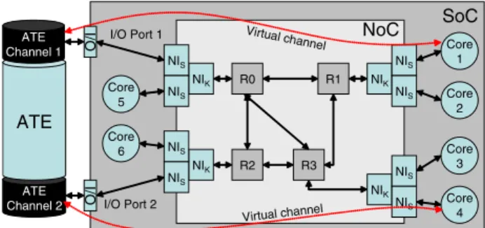
The proposed wrapper utilizes the functional communica- tion channel between a test source and a CUT. The delivery channel can be a dedicated path or a transparent virtual chan- nel. The wrapper is topology independent; it can be used for any NoC architecture as long as minimum sustainable band- width and latency are guaranteed during the test application of the target CUT. The quality-of-service guarantees ensure that the test data are available at the CUT at the right time. In this paper, the Æthereal [11, 12] NoC is used to explain the wrapper design and optimization.
The Æthereal NoC routers [11] provide both guaranteed and best-effort services. The guaranteed throughput (GT) router guarantees uncorrupted, lossless, and ordered data transfer, and both latency and throughput over a finite time in- terval. It also implements a network interface (NI) [12]—NI kernel and NI shells—which connects the network routers to 12th IEEE European Test Symposium (ETS'07), pp. 35-40, May, 2007.
NIK NIS NIS
Core 1
Core 2
NIK NIS NIS
Core 3
Core 4 NIK
NIS NIS Core
5
R2 NIK NIS NIS
R0 R1
R3 Core
6 I/O Port 1
I/O Port 2
NoC
I/OI/O
ATE Channel 2
ATE
ATE Channel 1
Virtual channel
Virtual channel SoC
Figure 1. NoC model based on the Æthereal NoC the IP cores by means of shared-memory abstraction (Fig. 1) utilizing a transaction-based protocol.
Figure 1 shows a NoC model based on the Æthereal ar- chitecture consisting of four GT routers . The NI supports multiple communication protocols required by the IP cores. Two of the NI shells are labelled I/O port 1 and I/O port 2, which can be used to interface the external ATE ports to the NoC. Two virtual channels (VC) are shown con- necting the ATE on port 1 to core 2 and the ATE on port 2 to core 3. Each VC is guaranteed a minimum bandwidth, . The term represents the max- imum link bandwidth between each pair of GT routers and along the VC path. If for some link
, the remaining can be allocated to other VCs in order to allow simultaneous test applications of multiple CUTs.
Figure 2 shows a simplified timing diagram of an AXI burst write transaction [22]. In order to reuse the NoC dur- ing test, the ATE needs to communicate with the CUT using the read/write transactions. Furthermore, the test methodol- ogy can be extended to reuse the embedded processors as test sources and sinks in place of the external ATE.
3. IP Core Model
IP core I/Os consist of primary inputs (PI), primary out- puts (PO), scan inputs (SI) and scan outputs (SO). A subset of the PIs can be categorized into primary data inputs (PDI) and primary control inputs (PCI). Assuming that the CUT communicates with the NoC by means of the AXI protocol (Fig. 2), PDI would be made up of WDATA[31:0] signals, while PCI consists of ADDR[31:0], AVALID, DLAST, and DVALID signals. Some PO signals can also be categorized
D(A0) D(A1) D(A2)
OK A
T0 T1 T2 T3 T4 T5 T6
CLK ADDR[31:0] AVALID WDATA[31:0] DLAST DVALID BRESP[1:0]
Figure 2. AXI burst-write transaction
Network Interface (input side)
PCI PDI
Network Interface (output side)
PCO
PDO PO’
IP Core
PI’
To other cores, POs, etc From other cores, PIs, etc
Internal scan chains
… … …
… … …
1 2 d
1 2 d
…
Figure 3. IP core model interfaced to the NI port into primary data outputs (PDO), consisting of RDATA[31:0] signals (not included in Fig. 2), and primary control outputs (PCO), consisting of BRESP[1:0] signals.
With the new classifications, core I/Os can be categorized as PDI, PDO, PCI, PCO, and other PI/POs which are not con- nected to the communication port of the NoC as shown in Fig. 3. The PDIs and PDOs are used to carry the test vec- tors from the ATE to the CUT, and the test responses from the CUT to the ATE, respectively. The PCIs and PCOs are needed to operate in the functional mode during the test ap- plication to ensure that the read/write transactions, by which the test data and responses are transmitted, execute properly. Since the CUT is not operating in the normal mode, the PCO signals must be generated by a wrapper controller. Special boundary cells proposed in [21] are used for PCOs to make the NoC operate in the normal mode to transfer the test re- sponses. For all other PI/POs, the IEEE 1500 boundary cells are used.
4. NoC Wrapper Architecture
Core wrapper design for a TAM-based test architecture has been explained in [2, 3]. For a CUT, given internal scan chains (ISC) of length, , primary inputs, pri- mary outputs, bidirectionals, and wrapper scan chains (WSC), the WSCs are formed while minimizing the maxi- mum scan-in and scan-out depths. Scan-in elements consist of zero or more inputs, bidirectionals, and ISCs. Scan-out elementsconsist of zero or more outputs, bidirectionals, and ISCs.
Figure 4 shows for a CUT with , and
flip-flops, , , and . The scan elements are optimally divided to form scan chains with maximum scan-in depth, , and maximum scan-out depth, , re- spectively; this is an optimal wrapper scan chain design [2]. As a result, the total test application time (TAT) can be calcu- lated by equation (1), where is the number of test vectors. For Fig. 4, the TAT is, clock cycles.
(1) When using TAMs as the delivery channel, the scan chain inputs and outputs are connected directly to the ATE input and output channels through the TAM wires. In order to reuse the
8
5 4
5 3
Scan-in depth, si,k
11 11 11
Scan-out depth, so,k 11 11 11
Figure 4. TAM-based wrapper scan chains made up of PI/PO boundary cells (square) and internal scan chains (rectangle)
NoC as the delivery channel, the scan chains are connected to the existing functional connections. Therefore, the test con- trol and synchronization are no longer at the hand of the ATE, rendering the IEEE 1500 wrapper inadequate. Sections 4.1– 4.3 explain how these problems are addressed in the proposed NoC wrappers.
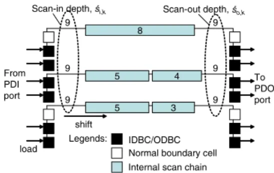
The proposed Type 1 wrapper uses the same approach as in [2, 3] when forming the wrapper scan chains which minimizes . For a given number of wrapper scan chains, , and the PDI bit-width, , the number of PDI bits that can be used to carry the test data for each wrapper scan chain, , is given by equation (2) [21]. To differentiate these PDI bits, those that can carry the test data are called input data boundary cells, IDBC (shaded black in Fig. 5). If
(Eqn. (3)), some PDI bits cannot be used to carry the test data. A similar analysis can be done for the output data boundary cells(ODBC), resulting in equations (4) and (5).
(2) (3) (4) (5) For the CUT with 8-bit PDI/PDOs, and three wrapper scan
chains (Fig. 5), means that each
wrapper scan chain is interfaced to two IDBC/ODBC cells.
In addition, means that the
remaining two PDI/PDO bits cannot be used to carry the test data. These unused PDI/PDO bits become part of the wrapper scan chain, with no extra functionality. Since in typical cases, the following discussion on the PDI on the input port also applies to the PDO on the output port.
During the test application, IDBC cells are loaded with the test data in one clock cycle, in the normal operation mode (refer to Fig. 5). The IDBC cells change into the test mode, during which the test data are serially shifted for two clock cycles to empty the contents into the scan chains. After com- pletion, the IDBC cells change again into the normal mode to capture the next incoming data from the PDI port. This op- eration is controlled by a test controller which keeps track of the number of loads and shifts using counters [23].
For the NoC wrapper with a scan-in depth of nine (Fig. 5), after four repetitions of loads and shifts, the first eight bits of
8
5 4
5 3
Scan-in depth, i,k 9
9
9
Scan-out depth, o,k 9
9
9 From
PDI port
To PDO port
shift
load IDBC/ODBCNormal boundary cell Legends:
Internal scan chain
Figure 5. Type 1 NoC wrapper architecture each scan chains are loaded with the test data. To load the last bit, the IDBC cells are loaded with new test data and a single shift clock is applied. However, before applying the capture cycle, the IDBC must also be loaded with valid test data. After the last single shift, only part of the IDBC cells contain valid test data. Reloading the IDBC data from the PDI port can corrupt the valid data currently in the IDBC cells.
To overcome this problem, the first shift cycles of every test pattern must shift in dummy bits into the scan chains. After the scan chains are completely loaded, an- other clock cycle is required to load the IDBC cells with valid test data before applying the capture cycle. Here, a formal definition of a new terminology based on this new scheme is given.
[Definition] The Scan-in (scan-out) elements for the Type 1 NoC wrapperconsist of the unused IDBC (ODBC) cells, bidirectional cells, and internal scan chains (i.e. excluding all the IDBC/ODBC cells). The maximum scan-in and scan-out depths are denoted by and , respectively (Fig. 5).
As a result of the new test scheme, the number of shift cycles required for the Type 1 NoC wrapper is summarized by equations (6) and (7). Equation (8) gives the total TAT, where the additional “ ” represents the final load of the IDBC data prior to the capture cycle. For the NoC wrapper in Fig. 5, clock cycles, smaller than based on equation (1).
(6) (7) (8)
For a CUT with wrapper scan chains and scan frequency, its scan rate/bandwidth is given by
. As shown in the previous example (Fig. 5), some PDI bits cannot be used to carry the test data due to the Type 1 wrapper’s input architecture constraint. In order to supply the test data to the CUT at rate, the required channel bandwidth on the NoC is given in equation (9). For the NoC wrapper in Fig. 5, the scan and required bandwidths are bits-per-second ( ) and , re- spectively.
0 1000 2000 3000 4000 5000 6000
2 4 6 8 10 12 14 16 18 20 22 24 26 28 30 32 34 36 38 40 42 44 46 48 50 52 54 56 58 60 62 64 Number of wrapper scan chains
Bandwidth (Mbps)
Scan bandwidth Required NoC bandwidth Test frequency = 100 MHz
Figure 6. Scan rate and required bandwidth of a Type 1 NoC wrapper for p93791’s Core 6 [25]
(9) Figure 6 shows the required bandwidth of the proposed Type 1 NoC wrapper (Fig. 5) compared to the actual scan bandwidth for an ITC’02 benchmark circuit. For some num- ber of wrapper scan chains, the required bandwidth is al- most twice that of the scan bandwidth. For these cases (i.e. ), the Type 1 NoC wrapper is inefficient in terms of NoC bandwidth utilization, similar to the NoC wrapper in [21]. For other cases, it is as efficient as the TAM-based wrapper while having the advantage of NoC reuse support ca- pability with minimal area overhead. In the next section, an alternate wrapper architecture is proposed to overcome this limitation.
Section 4.2 has shown that the Type 1 wrapper is inefficient in terms of bandwidth utilization. The Type 2 NoC wrapper in Fig. 7, is designed to complement the Type 1 wrapper in this aspect. Extra load/shift registers are added to the PDI/PDO ports, similar to the buffer architecture in [23] for the reuse of the SoC’s functional bus and the bandwidth matching reg- isters in [24]. The load/shift registers translate the PDI bit- width into the number of wrapper scan chains using parallel- serial shift registers. As a result, the required NoC bandwidth matches the scan bandwidth. The TAT for the Type 2 NoC wrapper is also the same as the TAM-based wrappers in equa- tion (1). This is achieved at the cost of area overhead of load/shift registers and a more complex control scheme to re- alize the bit-width conversion. Therefore, it is important that the Type 2 wrapper is used only when necessary. The next section looks at two proposed optimization schemes. 5. Optimization of the NoC Wrappers
Parallel core tests are performed according to an optimum test schedule under constraints. Figure 8 shows an example of a bin-packing optimization [2, 3], where a rectangle repre- sents the bandwidth-TAT ratio for every CUT. For an optimal packing, the new entry into the bin must be selected properly, which means that all possible bandwidth-TAT combinations must be explored. For optimum results, both the available test
8
5 4
5 3
Scan-in depth, si,k
11
11
11
Scan-out depth, so,k
shift
Load/shift register element Normal boundary cell Legends:
Internal scan chain 11
11
11
From PDI port To PDO port
load shift
Figure 7. Type 2 NoC wrapper with an I/O interface time ( or ) and bandwidth ( or ) must be consid- ered.
The problem of optimizing the number of wrapper scan chains ( ) is formally defined as follows.
: Given a core with functional inputs, functional out- puts, bidirectionals, internal scan chains of length , and a maximum bandwidth for the vir- tual channel between the core and the ATE, , find the number of wrapper scan chains, , such that ( ) the TAT is minimum, ( ) the required bandwidth, , and ( ) is minimum subject to ob- jectives ( ) and ( ).
: Given a core as in , and a maximum TAT, , find the number of wrapper scan chains, , such that ( ) the required bandwidth, , is minimum, ( ) TAT , and ( ) is minimum subject to objec- tives ( ) and ( ).
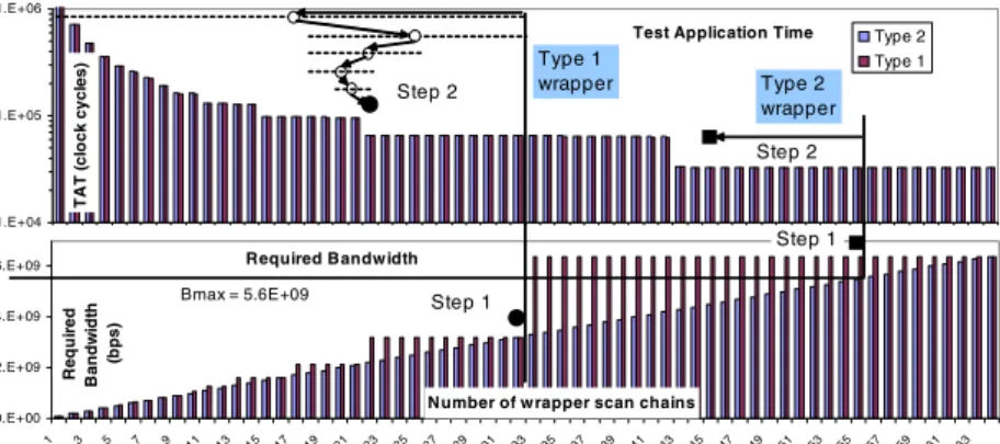
A similar problem for a TAM-based wrapper design has been proven to be NP-complete in [2]. Therefore, heuris- tic algorithms are proposed to solve both and . Fig- ure 9 illustrates graphically the search steps for (when ) for core 17 of the p93791 [25] bench- mark circuit. Since the TAT and the required bandwidth are monotonic decreasing and increasing with respect to , re- spectively, binary search algorithms can be used to find the optimal value of . At each search step, the optimal wrap- per scan chains which minimizes are formed us- ing the proposed algorithm in [2], described in Sect. 4. For the Type 1 wrapper, binary search takes place in steps 1 and 2 (refer to Fig. 9). In step 1, the maximum number of scan chains, , such that is located. In step 2, the search is restricted to to find the optimal
Core 1 Core 2
Core 3
Core 4
Bandwidth
Time T1
T2 B1
B2
Figure 8. Test schedule optimization
Table 1. p93791’s Core 6 [25] with 64-bit PDI/PDOs
TAM [2, 3] Type 1 NoC TAM [2, 3] Type 1 NoC 1 5,317,007 5,312,372 -0.09% 13 451,577 452,452 0.19% 2 2,658,613 2,656,404 -0.08% 14 451,358 451,576 0.05% 3 1,809,815 1,812,442 0.15% 15 447,197 448,072 0.20% 4 1,358,456 1,359,988 0.11% 16-19 341,858 342,076 0.06% 5 1,126,316 1,127,848 0.14% 20-21 337,478 338,134 0.19% 6 907,097 909,286 0.24% 22 333,317 333,754 0.13% 7 793,217 794,749 0.19% 23 231,478 231,258 -0.10% 8 679,337 680,212 0.13% 24-38 227,978 228,196 0.10% 9 674,957 676,489 0.23% 39-42 223,598 223,816 0.10% 10 565,457 566,770 0.23% 43-45 219,218 219,436 0.10% 11 561,077 562,171 0.19% 46 115,848 115,847 0.00% 12 455,738 455,956 0.05% 47-64 114,317 114,535 0.19%
% increase TAT (clock cycles) %
increase nsc
TAT (clock cycles) nsc
value for . The progression of the binary search is graphi- cally illustrated in Fig. 9. As a result, (Type 1) with a TAT of 65,098 clock cycles.
For the Type 2 wrapper, is directly calculated since is a linear function of . Binary search in step 2 (similar to the Type 1 wrapper) results in with a TAT of 32,766 clock cycles. Clearly a better result for the Type 2 wrapper. In this case ( ), the Type 1 wrapper is unable to utilize efficiently the allocated band- width because of the constraint in its I/O architecture.
A similar heuristic is implemented for and some se- lected cases for both algorithms are presented in Sect. 6. 6. Experimental Results
In order to evaluate the effectiveness of the proposed methodology, we have conducted experiments on three IP cores. Core 17 and core 6 (the largest of p93791 circuit) from the ITC’02 benchmark [25] are selected in order to offer comparisons with TAM-based approaches [2, 3]. Another IP core—an example core from [21]—allows some comparison with an NoC wrapper to be offered.
A TAT comparison between the proposed Type 1 NoC wrapper and TAM-based approaches is given in Table 1, for core 6 with bits. In all cases, the differences are always less than 0.25%; the proposed Type 1 NoC wrapper does not incur noticable penalty on the TAT. In fact, some re- ductions are achieved for and scan chains. For the Type 2 NoC wrapper, the TAT is the same as the TAM- based approach because the added interface between the CUT and the NoC port does not constraint the scan chain design. The Type 2 wrapper’s required bandwidth matches the scan bandwidth—an improvement due to the extra load/shift reg- isters.
For the circuit from [21], the TAT is given in Table 2. Com- pared to the TAM-based wrapper, the proposed Type 1 NoC wrapper is better for smaller number of wrapper scan chains. For wider scan chains, the TAT’s are about 3% longer. How- ever, compared to the NoC wrapper design in [21]1, the Type 1 wrapper is always superior.
1Based on the corrected results obtained from the paper author because of reporting error in the original published literature.
Table 2. TAT comparison for the circuit in [21]
Type 1 Type 2 Type 1 / TAM Type 1 / Amory
1 5,532 5,532 5,300 5,532 -4.19% -4.19%
2 2,771 2,771 2,660 2,771 -4.01% -4.01%
3 1,858 1,858 1,780 1,858 -4.20% -4.20%
4 1,396 1,451 1,428 1,396 2.29% -1.59%
5 1,363 1,429 1,406 1,363 3.15% -1.61%
6 1,363 1,418 1,395 1,363 2.35% -1.62%
% increase Proposed
nsc TAM [2, 3]
Amory [21]1
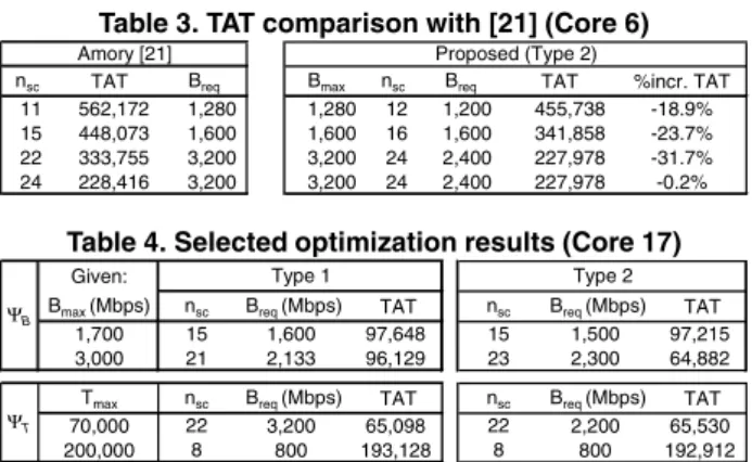
Further, we implemented the wrapper architecture pro- posed in [21] and compared the results (Table 3) for the a larger IP core (core 6 of p93791). The TAT and the required bandwidth, , (column 3) are obtained for selected
(column 1). Using (column 4) as input
to , the corresponding , , and TAT for the pro- posed Type 2 wrapper are obtained. Using at most the band- width required by [21], the proposed wrapper gives shorter TATs. For scan chains (last row), [21] requires 33% more bandwidth to obtain a comparable TAT.
Table 4 compares the Type 1 and Type 2 wrappers when
and are applied. For , both
wrappers result in similar performance—a slight advantage for Type 1 in terms of area overhead. At
, Type 2 is clearly the winner, with only 0.8% band- width overhead to achieve 32.5% TAT reductions. For , Type 2 requires 31% smaller bandwidth with less than 0.7% TAT overhead. On the other hand, at , Type 1 wrapper is superior due to its min- imal wrapper hardware overhead. The results illustrate the tradeoffs between the two types of NoC wrappers for a given constraint, which can be explored during the test schedule op- timization.
7. Conclusion
We have proposed two versions of the NoC wrapper that requires minimal overhead on the test application time and area overhead. The previously proposed wrapper design did not handle the problem of inefficient bandwidth utilization. In this paper, we have proposed two heuristics that find the optimal wrapper design for a given maximum bandwidth or maximum test application time—important for test schedule optimization.
Table 3. TAT comparison with [21] (Core 6)
nsc TAT Breq Bmax nsc Breq TAT %incr. TAT
11
562,172 1,280 1,280 12 1,200 455,738 -18.9% 15
448,073 1,600 1,600 16 1,600 341,858 -23.7% 22
333,755 3,200 3,200 24 2,400 227,978 -31.7% 24
228,416 3,200 3,200 24 2,400 227,978 -0.2% Proposed (Type 2)
Amory [21]
Table 4. Selected optimization results (Core 17)
Given:
Bmax (Mbps) nsc Breq (Mbps) TAT nsc Breq (Mbps) TAT
1,700 15 1,600 97,648 15 1,500 97,215
3,000 21 2,133 96,129 23 2,300 64,882
Tmax nsc Breq (Mbps) TAT nsc Breq (Mbps) TAT
70,000 22 3,200 65,098 22 2,200 65,530
200,000 8 800 193,128 8 800 192,912
Type 1 Type 2
ΨB
ΨT
Test Application Time
1.E+04 1.E+05 1.E+06
12345678910111213141516171819 2021 22 2324 25 2627 2829 3031 32 3334 35 3637 3839 4041 42 43 4445 4647 48 495051 52 53 5455 5657 58 596061 62 63 64
TAT (clock cycles)
Type 2 Type 1
Required Bandwidth
0.E+00 2.E+09 4.E+09 6.E+09
1 3 5 7 9 11 13 15 17 19 21 23 25 27 29 31 33 35 37 39 41 43 45 47 49 51 53 55 57 59 61 63
Number of wrapper scan chains Required Bandwidth (bps)
Bmax = 5.6E+09
Type 1
wrapper Type 2
wrapper
Step 1 Step 2
Step 1 Step 2
Figure 9. Optimization of NoC wrapper design for a given . In step 2 (Type 1), the dotted lines represent the search space which halves in every progression of the binary search
The proposed wrapper does not incur large test time over- head (against TAM-based designs) for the same number of wrapper scan chains (about 3% for a very small circuit, and less than 0.25% for larger circuits). The wrappers scale well for large circuits. The advantage of the proposed wrapper is that NoC reuse is possible with only small test time over- head. With additional allowances on the area overhead, the proposed wrapper (Type 2) can efficiently utilize the NoC bandwidth with zero overhead on the test application time. Acknowledgements
This work was supported in part by Japan Society for the Promotion of Science (JSPS) under Grants-in-Aid for Scien- tific Research B (No.15300018) and for Young Scientists B (No.18700046).
References
[1] L. Benini and G. D. Micheli, “Networks on Chips: A New SoC Paradigm”, IEEE Computer, 35(1), pp. 70-80, 2002.
[2] V. Iyengar, K. Chakrabarty, and E. J. Marinissen, “Test Wrapper and Test Access Mechanism Co-Optimization for System-on-Chip”, Journal of Electronic Testing: Theory and Applications 18, pp. 23-230, 2002. [3] S. K. Goel and E. J. Marinissen, “SoC Test Architecture Design for Ef-
ficient Utilization of Test Bandwidth”, ACM Trans. Design Automation of Electronic Systems, Vol. 8(4), Oct. 2003, pp. 399-429.
[4] E. Cota, L. Carro, and M. Lubaszewski, “Reusing and On-Chip Network for the Test of Core-Based Systems”, ACM Trans. Design Automation of Electronic Systems, Vol. 9, No. 4, October 2004, pp. 471-499. [5] A. M. Amory, E. Cota, M. Lubaszewski, and F. G. Moraes, “Reducing
Test Time With Processor Reuse in Network-on-Chip Based Systems”, In Proc. Integrated Circuits and Systems Design, 2004, pp. 111-116. [6] C. Liu, Z. Link, and D.K. Pradhan, “Reuse-Based Test Access and In-
tegrated Test Scheduling for Network-on-Chip”, In Proc. Design, Au- tomation and Test in Europe, 2006, pp. 303-308
[7] A. M. Amory, E. Briao, E. Cota, M. Lubaszewski, and F. G. Moraes, “A Scalable Test Strategy for Network-on-Chip Routers”, In Proc. IEEE International Test Conference, 2005, pp. 591-599.
[8] C. Grecu, P. Pande, A. Ivanov, and R. Saleh, “BIST for Network-on- Chip Interconnect Infrastructure”, VLSI Test Symposium, 2006, pp. 30- 35.
[9] E. J. Marinissen, R. Kapur, M. Lousberg, T. McLaurin, M. Ricchetti, and Y. Zorian, “On IEEE P1500 standard for embedded core test”, Jour- nal of Electronic Testing: Theory and Applications, 2002, pp. 365-383.
[10] P. Guerrier and A. Greiner”, A Generic Architecture for On-Chip Packet-Switched Interconnection”, In Proc. Design, Automation and Test in Europe, 2000, pp. 250-256.
[11] E. Rijpkema, “Trade Offs in the Design of a Router with both Guaran- teed and Best-Effort Services for Networks on Chip”, In Proc. Design, Automation and Test in Europe, 2003, pp. 10350-10355.
[12] A. Radulescu, et al., “An Efficient On-Chip NI Offering Guaranteed Services, Shared-Memory Abstraction, and Flexible Network Configu- ration”, IEEE Trans. Computer-Aided Design of Integrated Circuits and Systems, Vol. 24(1), pp. 4-17, Jan. 2005.
[13] C. A. Zeferino and A. A. Susin, “SoCIN: A Parametric and Scalable Network-on-Chip”, In Proc. Symposium on Integrated Circuits and Systems Design, 2003, pp. 169-174.
[14] M. Millberg, E. Nilsson, R. Thid, and A. Jantsch, “Guaranteed Band- width using Looped Containers in Temporally Disjoint Networks within the Nostrum Network on Chip”, In Proc. Design, Automation and Test in Europe, 2004, pp. 890-895.
[15] E. Bolotin, I. Cidon, R. Ginosar, and A. Kolodny, “QNOC: QoS Archi- tecture and Design Process for Network on Chip”, Journal of Systems Architecture: The Euromicro Journal, 50(23), pp. 105-128, Feb. 2004. [16] F. G. Moraes, N. Laert, V. Calazans, A. V. de Mello, L. H. Mller, L.
C. Ost, “HERMES: an Infrastructure for Low Area Overhead Packet- Switching Networks on Chip”, Integration, the VLSI Journal, 38(1), pp. 69-93, Oct. 2004.
[17] J. Bainbridge and S. Furber, “Chain: a Delay-Insensitive Chip Area Interconnect”, IEEE Micro, Vol. 22(5), pp. 16-23, Sept./Oct. 2002. [18] A. Lines, “Asynchronous Interconnect for Synchronous SoC Design”,
IEEE Micro, Vol. 24(1), pp. 32-41, Jan./Feb. 2004.
[19] E. Beigne, F. Clermidy, P. Vivet, A. Clouard, and M. Renaudin, “An Asynchronous NoC Architecture Providing Low Latency Service and its Multi-level Design Framework”, In Proc. IEEE Int’l Symposium on Asynchronous Circuits and Systems, 2005, pp. 54-63.
[20] X.-T. Tran, J. Durupt, F. Bertrand, V. Beroulle, and C. Robach, “A DFT Architecture for Asynchronous Networks-on-Chip”, In Proc. IEEE Eu- ropean Test Symposium, 2006, pp. 219-224.
[21] A. M. Amory, K. Goossens, E. J. Marinissen, M. Lubaszewski, and F. Moraes, “Wrapper Design for the Reuse of Networks-on-Chip as Test Access Mechanism”, European Test Symposium, 2006, pp. 213-218. [22] ARM, AMBA AXI Protocol Specification, March 2004.
[23] F. A. Hussin, T. Yoneda, A. Orailoglu, and H. Fujiwara, “Power- Constrained SOC Test Schedules Through Utilization of Functional Buses”, Int’l Conference on Computer Design, 2006, pp. 230-236. [24] A. Khoche, “Test Resource Partitioning for Scan Architectures using
Bandwidth Matching”, Digest of Workshop on Test Resource Partition- ing, 2002, pp. 1.4.1-1.4.8.
[25] E. J. Marinissen, V. Iyengar, and K. Chakrabarty, “A Set of Benchmarks For Modular Testing of SOCs”, In Proc. International Test Conference, 2002, pp. 519-528.
![Figure 6. Scan rate and required bandwidth of a Type 1 NoC wrapper for p93791’s Core 6 [25]](https://thumb-ap.123doks.com/thumbv2/123deta/5752807.27052/4.892.483.789.173.354/figure-scan-rate-required-bandwidth-type-wrapper-core.webp)