A Method of Test Generation for Path Delay Faults
Using Stuck-at Fault Test Generation Algorithms
Satoshi Ohtake†, Kouhei Ohtani‡ and Hideo Fujiwara†
† Graduate School of Information Science, Nara Institute of Science and Technology 8916-5 Takayama, Ikoma, Nara 630-0192, Japan
{ohtake, fujiwara}@is.aist-nara.ac.jp
‡ Hyper Device Division, Semiconductor Company, Sanyo Electronics Co., Ltd. 180 Ohmori, Anpachi-Cho, Anpachi-Gun, Gifu 503-0195, Japan
Abstract
In this paper, we propose a test generation method for non-robust path delay faults using stuck-at fault test gen- eration algorithms. In our method, we first transform an original combinational circuit into a circuit called apartial leaf-dag using path-leaf transformation. Then we generate test patterns using a stuck-at fault test generation algorithm for stuck-at faults in the partial leaf-dag. Finally we trans- form the test patterns into two-pattern tests for path delay faults in the original circuit. We prove the correctness of the approach and experimental results on several benchmark circuits show the effectiveness of it.
1. Introduction
For complex high speed VLSI circuits, delay testing is necessary to reach an acceptable quality level. Until now, many delay fault models have been investigated[1]. The path delay fault (PDF) model[2] is one of the most gen- eral models among them because distributed faults along paths can be tested and the delay size of detectable faults is scalable. However, the disadvantage with the PDF model is that the number of faults with respect to the number of gates in a circuit is exponential in the worst case and generating efficient (high fault coverage and compact) tests for faults in a short time is generally hard. In order to avoid the former disadvantage, a technique for selecting paths to be tested for combinational circuits[3] and tech- niques for re-synthesizing circuits such that the path count is reduced[4, 5] are proposed. The latter disadvantage can be avoided by synthesis-for-testability (SFT) techniques[1, 6], design-for-testability (DFT) techniques[1, 7] and circuit pseudo-transformationtechniques[1, 8, 9, 10, 11].
In this paper, we target to ease test generation. The SFT and DFT techniques can make a given combinational cir- cuit easily testable at the cost of additional hardware and in- creased delay. Therefore we aim to make a new test genera- tion methodology for PDFs in combinational circuits within
the framework of circuit pseudo-transformation. A circuit pseudo-transformation transforms a given circuit into dif- ferent one tentatively during test generation. And then tests are generated for the transformed circuit. After that, the generated tests for the transformed circuit are transformed into that for the original circuit.
Several test generation algorithms for PDFs in combina- tional circuits have been proposed[1]. A two-pattern test must be generated for a PDF to launch a signal transition at the primary input of a path. To deal with signal transitions, multiple-valued calculi, such as 10-value calculus[12] and 13-value calculus[13], are often used in PDF test generation algorithms. Such a multi-valued calculus increases the com- plexity of the test generation compared to the stuck-at fault (SAF) test generation. However, it was shown by Saldanha et al. that a single SAF test generation tool can be used for the generation of robust tests for a combinational circuit by transforming it into a rising(falling)-smooth-circuit[8]. The transformation is a kind of circuit pseudo-transformation. Since SAF test generation tools are mature and highly effi- cient, it is conceivable that utilizing a SAF test generation tool for PDF test generation is very effective. An alternative method was also proposed by Gharaybeh et al. [10] where a given circuit is transformed into a two-level circuit and then non-robust tests are generated by a single SAF test genera- tion tool. Although these methods can generate delay tests using single SAF test generation tools, they have the follow- ing disadvantages. For Saldanha’s method, only robust test generation is dealt with. However, it is necessary to gener- ate tests for non-robust testable PDFs to guarantee the qual- ity of circuits. For Gharaybeh’s methods, even if the num- ber of target paths for test generation is significantly smaller than the total number of paths, the complexity of their cir- cuit pseudo-transformation depends on the total number of paths in a given circuit.
Majumder et al.[11] considered a one-to-one correspon- dence between every untestable path in a circuit and a re- dundant SAF in its unfolded circuit. For well-well known Design Automation and Test in Europe 2003 (DATE03) , pp. 310-315, March 2003.
path delay fault classifications, they characterized each class in terms of the testability of SAFs in a circuit. The notion of the characterization is also related to this work.
The contribution of this paper is a new test genera- tion method for non-robust testable PDFs using an exist- ing single SAF test generation tool based on circuit pseudo- transformation. Our method deals with non-robust test gen- eration. We use a transformation called a path-leaf transfor- mationas circuit pseudo-transformation and we transform a given combinational circuit into a circuit called a partial leaf-dag. The complexity of the path-leaf transformation depends on the number of target paths for test generation instead of the total number of paths. In this paper, we theo- retically prove the correctness of the method and also show the effectiveness of it by performing several experiments on benchmark circuits. The experimental results show that our method can generate a test set with complete fault efficiency in short test generation time compared to a case using an ordinary commercial test generation tool. Furthermore, the test set generated by our method is significantly more com- pact than the one generated by the commercial tool.
2. Preliminary
A combinational circuit is composed of standard gates, such as AND, OR, NAND, NOR and NOT gates.
In a combinational circuit C, a path P is defined as an ordered set of gates{ f1,f2, . . . ,fn}, where f1is a primary input and fnis a primary output and the output of gate fiis the input to gate fi+1(1 ≤ i ≤ n−1). Path P has a delay fault if propagation time of a rising or a falling signal transition through the path exceeds a specified limit. Such a delay fault on a path is called a path delay fault (PDF)[2, 1]. A path delay fault on P is referred to as P↑ or P ↓, depending on whether the transition is rising or falling at fn.
A controlling value for fiis a value at its input that deter- mine the value at the output independent of the other inputs and is denoted as cv( fi). Inversely, a non-controlling value for fiis a value at its input which is not a controlling value of the gate and is denoted as ncv( fi). The input of ficonnected from fi−1is called an on-inputs of fialong P and denoted as on( fi,P). On the other hand, the inputs of fiother than fi−1 are called off-inputs of fialong P and denoted as off( fi,P). PDFs can be classified into four categories by the condi- tions of their off-inputs: (1) robust testable, (2) non-robust testable, (3) functional sensitizable and (4) functional un- sensitizable[1]. This paper targets (1) and (2) and does not distinguish them. Therefore, instead of using definition of non-robust off-inputand non-robust testability in [1], we re- define as follows.
Definition 1 Let { f1,f2, . . . ,fn} be a path in a combina- tional circuit C. Let gi jbe a gate such that gi j∈ off( fi). The off-input gi jis called a non-robust off-input with respect to an input vector pair⟨v1,v2⟩ for C if gi j(v2) = ncv( fi), where gi j(v2) is the value of gi jwhen v2is applied to C. ✷
1
2
3
4
5
6
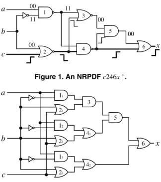
a b c
x
11
00
00 00
11
00
Figure 1. An NRPDF c246x↑. a
b
c
x
11
13
12
21
22
23
3
42
41
5
6
Figure 2. A full leaf-dag.
Definition 2 Let P= { f1,f2, . . . ,fn} and P ↑ (P ↓) be a path in a combinational circuit C and a PDF on P, respectively. The PDF P↑ (P ↓) is called a non-robust testable PDF (NR- PDF)if there exists an input vector pair⟨v1,v2⟩ of C such that at each fi∈ P, fi(v1) ̸= fi(v2) and gi j(v2) = ncv( fi) for each gi j∈ off( fi,P). Such an input vector pair is called a
non-robust two-pattern test. ✷
Example 1 A PDF c246x↑ shown in Figure 1 is an NRPDF because there is a two-pattern test⟨000,001⟩ and all the off- inputs meet the condition of non-robust off-input.
Definition 3 A full leaf-dag is a combinational circuit such that a fanout and an inverter are only permitted at the pri- mary inputs and the output of an inverter is not allowed to
have a fanout. ✷
Notice that full leaf-dag is originally referred to as leaf- dagin [9]. However, in this paper, to distinguish from par- tial leaf-dagdefined as follows, we call leaf-dag full leaf- dag.
Example 2 A full leaf-dag is shown in Figure 2.
Definition 4 Let α= {P1,P2, . . . ,Pm} be a subset of paths in a combinational circuit C. For each Pi∈ α, if there is no fanout and inverter on Piexcept for the primary input and an inverter is not allowed fanout, C is called a partial leaf-dag
with respect to α. ✷
Example 3 Consider a circuit shown in Figure 3. The cir- cuit is a partial leaf-dag with respect to c23426x.
Definition 5 A transformation from a combinational circuit Cto a partial leaf-dag with respect to a path P composed of the following two steps is called a path-leaf transformation with respect to P.
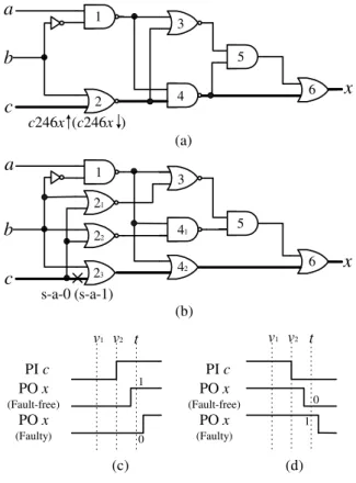
1
23
3
42
5
6
a
b
c x
41
21
22
Figure 3. A partial leaf-dag with respect to a path c23426x.
a
b
c d
b
c d a1
a2 a3
P P'
e
e
Figure 4. 1st step of path-leaf transformation: a fanout of a is moved to its input by duplicat- ing a to a1, a2and a3.
Step 1: Move all the fanouts on P to the primary input. From the primary output, each fanout on P is moved from an output of a gate to its input by duplicating the gate (see Figure 4.)
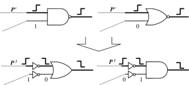
Step 2: Move all the inverters on P to the primary input. From the primary output, each inverter on P is moved from an output of a gate to its input by replacing AND (resp. OR) gate by OR (resp. AND) gate using De Morgan Law (see Figure 5.)
The path in the transformed circuit corresponding to P is
referred to as L(P). ✷
We consider a combinational circuit C and path P in C. Let CPl be a partial leaf-dag with respect to L(P) transformed from C with respect to P. Although the circuit structures of C and ClP are different, the functionalities of C and ClP are the same. There is one-to-one correspondence between paths P in C and L(P) in ClP.
Example 4 We obtain a partial leaf-dag with respect to c23426x shown in Figure 3 by applying the path-leaf trans- formation with respect to c246x to a combinational circuit shown in Figure 1.
Any combinational circuit can be transformed into par- tial leaf-dag with respect to its subset of paths by the path- leaf transformation. If we transform the circuit with respect to the set of its all the path, its full leaf-dag can be obtained. Definition 6 Let C be a partial leaf-dag with respect to α where α is a subset of paths. The I-edge of P∈ α in C refers to either the connection from primary input if no inverter is there, or else the connection immediately after the inverter.
✷
The I-edge is originally defined for full leaf-dag by Sal- danha et al.[8]. In order to apply this notion to partial leaf-
1 P'
1 0
0
0 1
P l P l
P'
Figure 5. 2nd step of path-leaf transformation: an inverter on a gate is moved to its input by changing the type of the gate.
dag, our definition overrides the definition by Saldanha et al.[8].
In general, to determine a path in a combinational circuit, all the gates on a path must be specified. However, for a full leaf-dag, if an I-edge is specified, the path which contains the I-edge is uniquely determined [9]. For a partial leaf-dag with respect to paths α, Pi∈ α is uniquely determined by specifying the I-edge on Pi.
3. Test Generation
In this section, we propose a test generation method for NRPDFs using a stuck-at fault (SAF) test generation algo- rithm. Given a combinational circuit C and a subset α of paths in C, the method proceeds as follows.
Step 1: We make a partial leaf-dag Cαl with respect to α by applying the path-leaf transformation scheme to C with respect to every path in α.
Step 2: For Clα, we generate tests for SAFs on I-edges cor- responding to paths in α using a single SAF test gen- eration algorithm.
Step 3: We transform the generated tests for the SAFs in Cαl into non-robust two-pattern tests for PDFs in C. Notice that, even if a PDF is robust testable, our method may generate a non-robust test for the PDF. If robust tests are required for robust testable PDFs, robust tests can be obtained by applying the method proposed by Saldanha et al.[8] prior to our method.
We explain our method in detail in the following subsec- tions. We first define correspondence between a PDF on P in C and an SAF on a I-edge of L(P) in Clα. Next, we de- fine a transformation which transforms a test pattern for the SAF in Cαl to a two-pattern test for the corresponding PDF on P in C. Then, to prove the correctness of the proposed method, we show reducibility between the test generation problem for an NRPDF in C and the test generation prob- lem for the corresponding SAF in Cαl.
3.1. Correspondence between PDF and SAF From the structural property of partial leaf-dag, for P∈ α if the I-edge of L(P) is specified, L(P) is uniquely deter-
mined in Cαl. In our test generation method, we target to generate a test for an SAF SA0 on the I-edge of L(P) in Cαl instead of a PDF P↑ on P in C. An SAF SA1 on the I-edge is also targeted instead of P↓ on P. The reason why we define such a correspondence between the PDF and the SAF is intuitively discussed in the following example. It is formally discussed in subsection 3.3.
Example 5 Consider a circuit shown in Figure 6(a). Fig- ure 6(b) is its partial leaf-dag with respect to c23426x(= L(c246x)) by applying the pah-leaf transformation to the circuit (a) with respect to c246x. In our test genera- tion method, SA0 (resp. SA1) on the I-edge of c23426x is targeted for the generation instead of c246x ↑ (resp. c246x↓). When a non-robust two-pattern test ⟨000,001⟩ (resp.⟨001,000⟩) is applied to the circuit (a), the faulty be- havior of a PDF c246x↑ (resp. c246x ↓) can be observed at the primary output x shown in (c) (resp. (d)). If there exists a PDF c23426x↑ (resp. c23426x↓) in the circuit (b), when the same two-pattern test is applied, the faulty behavior can also be observed at the primary output x shown in (c) (resp. (d)). If there exists an SAF SA0 (resp. SA1) on the I-edge of c23426x in the circuit (b), when the second vector of the two-pattern test 001 (resp. 000) is applied, the faulty behav- ior can be observed at the primary output x as 0 (resp. 1). The observed responses of the second vector for both the PDF and the SAF are the same.
3.2. Test pattern transformation
Let v and i be a test pattern for an SAF on the I-edge of L(P) in Cαl and the primary input of L(P). We transform v into a vector pair⟨ ˜v,v⟩ as a non-robust two-pattern test for the corresponding PDF on P in C, where ˜vdenotes that
˜
vi= ¯vifor the coordinate i of v and ˜vand ˜vj= vjfor each coordinate j other than i. Such a two-pattern test is reffered to as a single input change (SIC) two-pattern test. The rea- son why the transformed vector pair becomes a non-robust two-pattern test is described in subsection 3.3.
Example 6 Consider again the circuit shown in Figure 6(a) and (b). If a test pattern 001 (resp. 000) is generated to the SA0 (resp. SA1) on the I-edge of c23426x in the circuit of (b), the test pattern is transformed to a two-pattern test
⟨000,001⟩ (resp. ⟨001,000⟩) for the corresponding PDF on c246x of the circuit (a).
3.3. Correctness of the proposed method
In this section, we show the reducibility between the test generation problem for SA0 (resp. SA1) on the I-edge of L(P) in Cαl and the test generation problem for P↑ (resp. P↓) on P in C.
Theorem 1 A vector pair⟨ ˜v,v⟩ of C is an SIC non-robust two-pattern test for P↑ (resp. P ↓) on P if and only if there exists a test v of Cαl for SA0 (resp. SA1) on the I-edge of L(P).
1
2
3
4
5
6
a
b
c
x
1
23
3
42
5
6
a
b
c
x
41 21
22
v1 v2 t v1 v2 t
1
1 0
0
s-a-0 (s-a-1)
(c) (d)
(b) (a) c246x (c246x )
PI c PO x
(Fault-free)
PO x
(Faulty)
PI c PO x
(Fault-free)
PO x
(Faulty)
Figure 6. (a) a PDF c246x↑ (c246x ↓) of a cir- cuit, (b) its corresponding SA0 (resp. SA1) fault in the partial leaf-dag of the ciruit of (a) with respect to c246x, and (c) and (d) are faulty behaviors of c246x↑ and c246x ↓, respectivery.
Proof: We show that a vector pair⟨ ˜v,v⟩ of C is an SIC non-robust two-pattern test for P↑ on P if and only if there exists a test v of Cαl for SA0 on the I-edge e of L(P). If part: An input vector v of Cαl is a test for SA0 on e. If vis applied to Clα, for each gate fl∈ L(P), gl(v) = ncv( fl) because v is a test for SA0 on e, where gl= off( fl). If v is applied to C, for each gate f ∈ P, g(v) = ncv( f ), where g= off( f ), because, from Definition 5, L(P) is obtained by moving all the inverters on P to the primary input of P. Therefore, if a vector pair whose second vector is v is applied to C, all the off-input of P meets the condition of Definition 1. Here, let i be the primary input of P. The primary input of L(P) is also i because the primary input is unchanged by the path-leaf transformation of Definition 5. Since v is a test for SA0 on e, v makes e should be 1 if v is applied to Cαl. If ˜v is applied as a first vector of the vector pair, the logic value on e becomes 0. There- fore, if the vector pair⟨ ˜v,v⟩ is applied to Clα, a rising tran- sition is induced at e. The rising transition is propagated to the primary output of L(P) because there is no inverter on the partial path from e to the primary output. From
Definition 5, for each on-input fl∈ L(P) in Cαl, if a tran- sition ncv( fl) → cv( fl) (resp. cv( fl) → ncv( fl)) occurs, ncv( f ) → cv( f ) (resp. cv( f ) → ncv( f )) also occurs at the corresponding on-input f ∈ P in C (see Figure 5). There- fore, if⟨ ˜v,v⟩ is applied to C, some transition is propagated through P and the rising transition is induced at the primary output of P. Since the rising transition occurs at the output of P and all the off-input of P meet the condition of non- robust off-input, the vector pair⟨ ˜v,v⟩ is an SIC non-robust two-pattern test for P↑ on P in C.
Only if part: An input vector pair⟨ ˜v,v⟩ of C is an SIC non-robust two-pattern test for P↑ on P. If ⟨ ˜v,v⟩ is ap- plied to C, some transition is propagated through P and the rising transition is induced at the primary output of P. From Definition 5, for each on-input f ∈ P in C, if a transition ncv( f ) → cv( f ) (resp. cv( f ) → ncv( f )) occurs, ncv( fl) → cv( fl) (resp. cv( fl) → ncv( fl)) also occurs at the corresponding on-input fl∈ L(P) in Cαl (see Figure 5). If the second vector v is applied to Clα, the logic value 1 is appeared at the primary output of L(P). Since there is no in- verter on the partial path from e to the primary output, SA0 in e is activated by applying v. Since all the off-inputs of P meet the condition of Definition 1 when⟨ ˜v,v⟩ is applied to C, each off-input of L(P) becomes a non-controlloing value when v is applied to Cαl. Therefore, the vector v is a test for SA0 on e of L(P) in Cαl.
We show that a vector pair ⟨ ˜v,v⟩ of C is an SIC non- robust two-pattern test for P↑ on P if and only if there exists a test v of Clαfor SA0 on the I-edge e of L(P). It is obvious that there exists a similar correspondence between P↓ on P and SA1 on e. Thus, the theorem holds. ✷ Lemma 1 A PDF P↑ (P ↓) is non-robust testable if and only if there exists an SIC non-robust two-pattern test for P↑ (P ↓) [10].
The proof of Lemma 1 is available in [10].
Theorem 2 The test generation problem for P↑ (resp. P ↓) on P∈ α in C can be reduced to the test generation problem for SA0 (resp. SA1) on the I-edge of L(P) in Cαl.
Proof: From Lemma 1 and Theorem 2, it is obvious that the test generation problem for P↑ (resp. P ↓) on P ∈ α of C can be reduced to the test generation problem for SA0 (resp. SA1) on the I-edge of L(P) in Clα. ✷
4. Experimental Results
We evaluate effectiveness of the test generation method proposed in the previous section by experiments and discuss the advantages of the method. In the experiments, we used circuits from the ISCAS’85 benchmark suite and the com- binational logic of circuits from the ISCAS’89 benchmark suite. Both the ordinary PDF test generation method and our proposed test generation method are applied to these circuits. The PDF test generation tool of TestGen (Synop- sys) [14] is used as an ordinary PDF test generation algo- rithm and the SAF test generation tool of TestGen is used as
the SAF test generation algorithm in our proposed method. Both tools are used on Ultra 30 (Sun Microsystems). In the experiments, we did not select paths to be targeted for test generation and thus we targeted all paths in test generation because the selection is not essential for the experiments.
Table 1 gives the results of both the ordinary test genera- tion and our proposed method. In the table, columns in “Cir- cuits” represent test generation results for each circuit. For each row, test generation results for both the ordinary test generation denoted as “Ordinary” and our proposed method denoted as “Proposed” are available.
Row “# Faults” denotes the number of faults targeted in test generation. For the ordinary test generation, TestGen did not list all the faults that should be tested for s1488, s1494, s838.1 and c880. Sub-row “Proposed” shows the total numbers of paths in the circuits. The number is also the total number of SAFs on I-edges in the circuits.
Rows “# Testable Faults” and “# Two-Pattern Tests” de- note the number of non-robust testable faults for which two- pattern tests were generated and the number of two-pattern tests. For all the circuits, the ordinary test generation tool achieved complete fault efficiency with respect to the listed PDFs for all the circuits. The SAF test generation tool also achieved complete fault efficiency with respect to all the SAFs on I-edges of all the transformed circuits, that is, our proposed method achieved complete fault efficiency with respect to all the PDFs of all the circuits. The average num- ber of faults detected per a two-pattern test for the ordinary test generation method is 1.03 and that for our proposed method is 6.15. Therefore, we can say test sets generated by our proposed method is more compact than that generated by the ordinary method. We believe that utilizing stuck-at fault simulation induced the good results instead of using more restricted path delay fault simulation.
Row “Test Generation Time (sec.)” denotes test genera- tion time in second. The test generation time of our method is shorter than the ordinary one except for c880. For c880, although the number of faults listed by TestGen is 1/4 of the number of faults considered in our method, test generation time of our method is only double of that of TestGen.
Sub-rows “Ordinary” and “Proposed” in “Time Required for Listing Faults (sec.)” denote times required for making a file of a path delay fault list for a circuit by TestGen and for transforming a circuit into its full leaf-dag by our method, respectively. Time required for transforming a circuit into its full leaf-dag is shorter that that for listing paths by Test- Gen for most circuits.
Row “Circuit Size (#gates)” denotes the original circuit sizes of benchmark circuits for “Ordinary” and the circuit sizes of transformed circuits by the path-leaf transformation for “Proposed”. In this experiments, we did not select the paths to be tested. Therefore, the size of transformed cir- cuits became large compared to the original one. However, it is easily considerable that if the number of paths to be tested in a circuit is a tractable number, the complexity of
Table 1. Experimental results. Circuits
c17 s386 s382 s526 s1488 s1494 s838.1 c880
# Faults Ordinary 22 414 800 820 1788 1802 2876 4520
Proposed 22 414 800 820 1924 1952 3428 17284
# Testable Faults Ordinary 22 414 734 720 1781 1781 2876 4477
Proposed 22 414 734 720 1916 1927 3428 16652
# Two-Pattern Tests OrdinaryProposed 229 37278 69992 69899 1754214 1754205 11442876 44323451
Test Generation Ordinary 0.16 1.47 4.25 4.59 20.77 20.51 63.80 121.12
Time (sec.) Proposed 0.15 0.36 1.39 1.53 1.62 1.70 15.45 238.36
Time Required for Ordinary 0.04 0.23 0.52 0.53 2.21 2.27 5.07 13.91
Listing Faults (sec.) Proposed 0.39 0.40 0.45 0.46 0.50 0.50 0.51 0.79
Circuit Size (#gates) Ordinary 6 159 158 193 653 647 446 352
Proposed 15 206 494 431 1262 1282 2257 9772
applying the path-leaf transformation is also tractable and thus the size of the transformed circuit is also tractable.
From the above discussion, our test generation method is superior to the ordinary test generation for those benchmark circuits.
5. Conclusion
In this paper, we proposed a test generation method for path delay faults. In the method, a single stuck-at fault test generation tool is used to generate non-robust two-pattern tests instead of a path delay fault test generation tool. The advantage of the method is that non-robust test genera- tion is dealt with and the complexity of the circuit pseudo- transformation in the method depends on the number of tar- get paths for test generation instead of the total number of paths in a circuit. We theoretically proved the correctness of the method and showed the effectiveness of it through experiments. We confirmed that test generation time re- quired for guaranteeing complete fault efficiency and the number of non-robust two-pattern tests to achieve complete fault coverage by using the method can be reduced com- pared to those by an path delay fault test generation tool.
Our future work is to ease the test generation problem for functional testable path delay faults by using a stuck-at fault test generation tool under the concept of circuit pseudo- transformation.
References
[1] A. Krsti´c and K.-T. T. Cheng: Delay fault testing for VLSI circuits, Kluwer Academic Publishers, 1998.
[2] G. L. Smith: “Model for delay faults based upon paths,” in Proc. of Int. Test Conf., pp. 342–349, 1985.
[3] K. Heragu, V. D. Agrawal and M. L. Bushnell: “Statistical methods for delay fault coverage analysis,” in Proc. of VLSI Design, pp. 166–170, 1995.
[4] A. Krsti´c and K.-T. T. Cheng: “Resynthesis of combina- tional circuits for path count reduction and for path de-
lay fault testability,” in Proc. of European Design and Test Conf., pp. 486–490, 1996.
[5] I. Pomeranz and S. M. Reddy: “On synthesis-for testabil- ity of combinational logic circuits,” in Proc. of 32nd Design Automation Conf., pp. 126–132, 1995.
[6] A. K. Pramanick and S. M. Reddy: “On the design of path delay fault testable combinational circuits,” in Proc. of 20th Fault Tolerant Computing Symp., pp. 374–381, 1990. [7] P. Uppaluri, U. Sparmann and I. Pomeranz: “On minimizing
the number of test points needed to achieve complete robust path delay fault testability,” in Proc. of VLSI Test Symp., pp. 288–295, 1996.
[8] A. Saldanha, R. K. Brayton and A. L. Sangiovanni- Vincentelli: “Equivalence of robust delay-fault and sin- gle stuck-fault test generation,” in Proc. of Int. Conf. on Computer-Aided Design, pp. 418–421, 1992.
[9] W. K. C. Lam and R. K. Brayton: Timed Boolean Functions: A Unified Formalism for Exact Timing Analysis, Kluwer Academic Publishers, 1994.
[10] M. A. Gharaybeh, M. L. Bushnell and V. D. Agrawal: “Clas- sification and test generation for path-delay faults using sin- gle stuck-at tests,” Journal of Electronic Testing: Theory and Applications, Vol. 11, No. 1, pp. 55–67, Aug. 1997. [11] S. Majumder, B. B. Bhattacharya, V. D. Agrawal and M. L.
Bushnell: “A complete characterization of path delay faults through stuck-at faults,” in Proc. of Int. Conf. on VLSI De- sign, pp. 492–497, 1999.
[12] K. Fuchs, F. Fink and M. H. Schulz: “DYNAMITE: An ef- ficient automatic test pattern generation system for path de- lay faults,” IEEE Transactions on Computer-Aided Design of Integrated Circuits and Systems, Vol. 10, No. 9, pp. 1323– 1335, Oct. 1991.
[13] T. J. Chakraborty, V. D. Agrawal and M. L. Bushnell: “De- lay fault models and test generation for random sequential circuits,” in Proc. of Design Automation Conf., pp. 165–172, 1992.
[14] Synopsys, Inc.: TestGen Tool Reference Manual Version 1999.10-TG4.1, 1999.