Capture in Turn Scan for Reduction of Test Data Volume,
Test Application Time and Test Power
Zhiqiang You1 Jiedi Huang2 Michiko Inoue3 Jishun Kuang2 Hideo Fujiwara3 1. Software School, Hunan University, Changsha, China,[email protected] 2.School of Computer and Communication, Hunan University, Changsha, China
3. Nara Institute of Science and Technology, Ikoma, Japan
Abstract-With the exponential increase of transistor counts, scan design encounters several problems such as large test data volume, long test application time and high test power. In this paper, we propose a new method to reduce test data volume, test application time and also average and peak power during test. The proposed method is based on a scan chain disabling technique where only one internal sub scan chain is active at a time. Though our method makes a sacrifice of test generation time, instead, we can achieve reduction of test data volume, test application time and test power together. Experimental results show the effectiveness of the proposed method.
Keywords-design for testability, scan chain disabling, low power testing, test generation, test volume reduction.
I. INTRODUCTION
With the exponential increase of transistor counts, scan design encounters several problems such as large test data volume, long test application time and high test power. To resolve these problems, several methods have been proposed. However, these methods tend to focus on some of the problems, and sometimes work worse for other problems.
Several scan architectures based on multiple internal scan chain design have been proposed to reduce test data volume and test application time. The method in [1] effectively reduces test data volume and test application time using a reconfigurable switch to apply tests from a limited number of external inputs to a large number of internal scan chains. VirtualScan technology[2]reduces test data volume and test application time by splitting long scan chains into multiple short internal scan chains. CircularScan architecture[3] reduces test data volume and test application time by utilizes captured responses for the next test vector. Scalable Adaptive Scan[4] reduces test data and test application time in a hierarchical and low pin count environment. However, these techniques are not efficient in test power reduction.
A power issue is another concern for scan test. High power dissipation during scan test may give rise to severe hazards in circuit reliability or provoke instant circuit damage[5]. Various techniques have been proposed to reduce average power by reducing switching activity during scan shift operation. The methodologies in [6] employ test vector and scan cell reordering technique. The methodologies in [7] also consider test compaction by exploring the correlation between consecutive test patterns. Scan chain disabling technique[8]reduces test power drastically. In this technique, only one scan chain is activated at a time during scan shifting. The power during scan shifting is reduced to 1/N, where N is the number of internal sub-scan chains. However, during capture cycle, all the sub-scan chains are active, and peak
power is not reduced. High peak current demands may cause IR drop so that good chips fail to at-speed testing.
Recently, many techniques have been proposed to reduce peak power dissipation. X-filling techniques[9] efficiently reduce capture or peak power dissipation by filling don’t care bits appropriately. We previously proposed a low test power method[10]based on scan chain disabling technique. In this technique, the scan cells are grouped into N internal sub-scan chains. Both peak and average power dissipation are reduced by activating only one scan chain at a time during both shift and capture cycles. However, the above low peak power methods do not work efficiently for test data volume or test application time reduction.
In this paper, we propose a new scan test scheme, capture in turn scan test scheme (CTS). The proposed scheme is based on scan chain disabling technique where only one internal sub-scan chain is active in both shift and capture cycles and both average and peak test powers are reduced. In this paper, we adopt a strategy that we firstly configure internal sub-scan chains and secondly generate test patterns customized to the configured scan chains. This idea makes best use of test pattern flexibility that is the same fault can be detected by several test patterns and the same test pattern can propagate errors of the same fault to several outputs. Though test patterns have to be generated under a constraint on highly restricted scan chain activity in the proposed scheme, the test pattern flexibility works well for test generation. As a result, we can achieve reduction of test data volume and test application time in addition to reduction of average and peak test power.
The rest of the paper is organized as follows. A novel test scheme CTS and a test generation method for CTS are proposed in Sections 2 and 3 respectively. Section 4 shows the experimental results and the paper is concluded in Section 5.
II. CAPTURE INTURNSCANTESTSCHEME
A. The Previous Method
In [10], we previously proposed a low power scan test scheme for a given test set. In this scheme, one scan chain is divided into N internal sub-scan chains. Their test pattern is also divided into N sub patterns and shifted into N sub-scan chains one by one. The proposed scheme adds a clock controller, a MUX, a test mode pin TC and
logN
bits control signals Cs to select one active internal sub-scan chain. Since this scan shift-in operation requires the same cycles as one scan chain configuration but activates a part of circuit at a time, average test power is reduced. In addition, only one scan chain captures the test response at a time, and therefore, peak power is also reduced.2010 19th IEEE Asian Test Symposium
1081-7735/10 $26.00 © 2010 IEEE DOI 10.1109/ATS.2010.70
371
In [10], we also proposed a method to determine sub- scan chain configuration and the sub-scan chains that capture test responses for a given test set. The proposed method utilized don't care information and the detect- capture information of a given test set to avoid unnecessary shift-in or shift-out. However, it may require more test data volume and test application time than one scan chain configuration. In addition, the scheme includes the sub-scan chain selection signals in a test data. Therefore, more test volume is required.
B. Capture in Turn Scan Test Scheme
In this subsection, we propose a capture in turn scan test scheme(CTS). As mentioned before, the previous proposed scheme does not work well for test application time or test data volume reduction due to the test pattern restoring and the scan chain selection signals. In CTS, we resolve these problems by the following ideas.
1. The test pattern restoring is required in the previous scheme since sub-scan chains are configured for a given test set. In CTS, we have an opposite strategy that we first configure sub-scan chains without any information on test patterns, and then generate test patterns customized to the configured sub-scan chains. The test generation under constraint on sub-scan chain activity can find test patterns that do not require test pattern restoring.
2. To reduce test data volume, we do not select an active scan chain from the outside of the circuit. Instead, we activate sub-scan chains in turn cyclically.
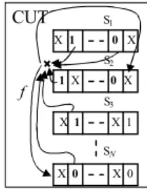
We propose the following test flow to realize the above ideas. Let S1, S2, …, SN be sub-scan chains. First, the test vector for S1 is shifted. After that, S2 becomes active to capture its test response. Then, we shift a new test vector into S2while shifting out the test response. We execute this test flow cyclically until there is no test vector to be applied.
Based on the test flow, we propose a CTS test scheme as shown in Fig. 1. In CTS, the flip-flops in the circuit under test (CUT) are grouped into N internal sub-scan chains, where the flip-flop groups can be determined arbitrarily. The additional hardware of this scheme is a test mode pin TC, an N-bits cyclic shift register (CSR), N AND gates, a NOT gate and an N-to-1 MUX.
During scan test (TC=1), only one sub-scan chain is active to shift in/out test vectors/responses or capture a test response at a time. The CSR controls the clocks of all sub- scan chains. At the beginning of test, we initialize the CSR so that only one bit is 1 and the other bits are 0’s. Through a NOT gate, Scan_En controls the clock of the CSR. For example, if the values in the CSR are 10…0, that is, C1=1, C2,…,CN=0. Only the clock of S1is not gated. The clocks of other sub-scan chains are disabled by their AND gates. We can shift in the test vector into S1while shifting out a test response captured in S1 via the MUX. After the vector in S1is shifted in, Scan_En is reset to 0. The CSR is cyclic right shifted one bit by the clock signal Scan_En. The values in CSR turns into 010…0, that is C1=0, C2=1,…,CN=0. At this time, S2captures a test response. After that, Scan_En is set to 1. The test vector of S2is shifted in while shifting out the captured test response. We repeat this test procedure until all the test vectors are applied.
Figure 1. Capture in turn scan test scheme.
The test pin overhead is only the test mode pin TC which holds 1 during scan test. In the proposed method, we make sub-chains active cyclically and regularly. Therefore, we do not need to control the active sub-chain from the outside and hence can reduce test data volume.
III.CAPTURE INTURNSCANTESTGENERATIONSCHEME
We then propose a test generation method for CTS. Firstly, a test vector for S1is generated. At this time, the values in S2,…,SNare X’s and only the test response at S2is observed. We apply fault simulation to remove the faults detected by this vector. Then, the test vector for S2and the X bits in S1 is generated. The scan cells which have specified values in S1 keep their values, the values in S3,…,SNare still X’s and the test response at S3is observed. We apply fault simulation to remove the faults detected by the vector. The test procedure continues until all the detectable faults of a CUT are detected.
The test generation method is more efficient to have short test application time than that in the previous scheme. Instead of restoring the test vectors, we apply a new test vector for a sub-scan chain. For example, as shown in Fig. 2, we assume that some care bits are needed in a test vector to detect a fault f. The bold values are only contributed to the detection of f. The errors of f can be propagated to S2and SN. After S2captures the test response, we do not need the care bits in the test vector of S2any more. A new test vector can detect more new faults using this proposed test generation scheme.
Figure 2. An example of test information for fault f.
In general, in full scan design with single scan chain, there is a capture cycle after shifting a whole test vector into all the scan cells. However, in this scheme, a capture cycle of a sub-scan chain is performed after shifting a test vector into one sub-scan chain. The chance to update the test vectors in the sub-scan chains is increased N-1 times. Since errors of the same fault may be propagated into two or more sub-scan chains by a test pattern, observation of one sub-
CLK Scan-in PIs
POs
Tester CUT S1
SN
Scan-out
MUX
Scan_En
TC CSR
CUT
f
S1
X 1 0 X
SN X 0 X 0
S2
1 X 0 X
S3 X 1 X 1
372
scan chain may detect more than 1/N faults detected by the test if all the sub-scan chains are observed, and N capture cycles may observe more faults than that of one test vector can detect in conventional scan chain design. Therefore, the proposed test generation method may achieve shorter test application time.
We call the shifted values into the activated sub-scan chain a test slice for a test vector. For example, Fig. 3(a) shows the test vectors of a CUT. The CUT has 8 scan cells, 4 sub-scan chains and 10 test vectors. The bold letters denote the active scan chain to capture its test response for that test vector. The test slice in the first vector is the left two bits “11”. The test slices of Fig. 3(a) are shown in Fig.3(b). The test slices according to its order can be lined into a test line. For instance, the test line is 11011000011101101010 in this example. The tester only needs to store the test line.
XX XX XX XX
11 XX XX XX 11
11 0 1 XX XX 01 11 0 1 1 0 XX 10 11 0 1 1 0 0 0 00 01 0 1 1 0 0 0 01 01 1 1 1 0 0 0 11 01 1 1 0 1 0 0 01 01 1 1 0 1 1 0 10 10 1 1 0 1 1 0 10 10 1 0 0 1 1 0 10 (a) test vectors. (b) test slices. Figure 3. An example of a test.
IV. EXPERIMENTALRESULTS
We have conducted experiments on the full scan version of ISCAS’89 benchmark circuits using TetraMAX (Synopsys) on Sun Fire X4100. In the experiments, the primary inputs (PIs) and primary inputs (POs) of a CUT are regarded as scan cells.
A.Results Using TetraMAX
Usually test generation time and test application time are trade-off factors. MT-Filling for don’t care values can reduce test power, while random filling is effective for test application time reduction. This experiment will also show the trade-offs.
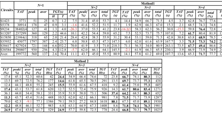
Table 1 describes the test application time and test power reductions for the test set using MT-filling. Since TetraMAX cannot realize MT-filling to the test vectors for PIs, we apply MT-filling after test generation. After that, we apply fault simulation to remove the test slices which cannot detect new faults. The first column gives the circuit’s names. The second big column gives the results for the full scan circuits with single scan chain. Its five sub-columns give the test application time (“TAT”), peak power (“peak”), average power (“aver”), and the test generation time (“TGT”) including fault simulation using HOPE (“H”) or using TetraMAX (“T”). Compared the last two sub-columns in the big column, we find that TetraMAX fails to have short test generation time. The last two big columns show the reduction of test application time (“TAT(%)”), peak power
“peak(%)”, average power “aver(%)”, total test power
“total(%)”), and its test generation time for N=2,3,4 respectively for our proposed scheme. In the test generation of the first big column (“Method 1”), only one vector is generated when performing ATPG. However, in the last big
column (“Method 2”), we generate the test cubes which can detect all the detectable faults. After applying fault simulation, we select the best one which can detect the most new faults from the top 400 test cubes if the number of test cubes is lager than 400 due to the memory limit.
From this table, we can see that Method 1 efficiently reduces test application time compared with that of conventional scan chain design. The percentages of test application time reduction are 11.1%, 14.1% and 13.6% in average when N=2,3,4. Method 2 is more efficient in test application time reduction than Method 1. The test application time can be reduced to 24.9%, 24.9% and 24.4% in average when N=2,3,4. The values in the left parenthesis of the column “TAT” or “TAT(%)” are the number of untestable collapsed faults. For s9234 when N=1, four collapsed faults are escaped to be detected. For the same circuit, when N=3 for Method 1 the number of untestable collapsed faults is 3. For s15850 when N=1, the number of escaped collapsed faults is 1. Therefore, compared with the same kind of test generation results, our methods can achieve higher fault coverage.
Though the results for single scan chain design use MT- filling technique which efficiently reduces test power especially average power, Method 1 and Method 2 can reduce peak and average power drastically. The reduction ratios are a little lower than 1-1/N for N=2, 3 and 4 in average. The total test power is reduce more than average power due to the test application time reduction.
The test generation time of Method 1 and Method 2 is long. These are the trade-offs between test generation time, test application time and test power. Notice that the test generation flows of them are complicated, and TetraMAX may fail to have short test generation time. In another words, it may achieve short test generation time to develop a test generation tool which adapts the proposed test generation scheme.
Table 2 shows the results of random filling compared to those of MT-filling for conventional scan chain design. The results show the trade-offs between test application time and test power. Compared to the random filling method with conventional scan chain design (Tables 1 and 2), we can find Method 2 is more efficient to reduce test application time. The test power also can be reduced more.
TABLE II THE RESULTS FOR CONVENTIONAL SCAN CHAIN DESIGN USING RANDOM FILLING.
Circuits TAT (%) peak (%) aver (%) total (%) TGT(s)
S1423 7.3 -9.8 -67.5 -55.3 0.03
S5378 7.4 25.8 -114.5 -98.6 0.12
S9234 3.9 -11.0 -172.3 -161.6 0.33
S13207 10.7 -20.6 -193.3 -162.0 0.43
S15850 27.1 -18.6 -3716 -243.9 0.47
S35932 -13.6 7.2 -126.2 -157.1 0.68
S38417 77.9 -27.2 -456.1 -22.9 1.15
S38584 13.7 -7.5 -219.9 -176.1 1.29
Aver. 16.8 -7.7 -215.2 -134.7 0.56
B. Comparison with Our Previous Method
As mentioned in Section 2, our previous method does not work well for test data volume or test application time reduction. For s9234, when N=4, the test data volume is
373
increased to 321.8% compared with the conventional scan chain design.
Table 3 shows the test application time and test data volume reduction of our proposed method compared with the conventional scan chain design using TetraMAX. Here, we only give the results of the circuits using in our previous method[10]. Since tester does not need store control signals to test the circuits, the test data volume reduction equals that of test application time. This table shows that the percentages of test application time and test data volume reductions are 15.7%, 17.5% and 15.8% in average for N=2,3,4 respectively. Our proposed approach can efficiently reduce test application time and test data volume.
TABLE III. TEST APPLICATION TIME REDUCTION IN THE PROPOSED METHOD. TAT/TDV reduction (%)
Circuits
N=2 N=3 N=4
s1423 17.4 24.4 23.8
S9234 12.4 15.5 9.2
S13207 17.4 12.7 14.3
Aver 15.7 17.5 15.8
V. CONCLUSIONS
This paper proposed a new scan test scheme CTS. CTS efficiently reduces test data volume, test application time and peak and average test power. Compared with our previous scheme, this scheme has low hardware and test pin overheads.
In the proposed test scheme, one scan chain is divided into N internal sub-scan chains. We found that, with N increases, the reduction of peak, average, total power dissipation increases. However, more sub-scan chains may cause more hardware overhead and high layout complexity.
We can explore the trade-offs between the mentioned factors when designing a circuit.
ACKNOWLEDGMENT
This paper was supported by the National Natural Science Foundation of China (NSFC) under grant No. 60673085, 60773207.
[1] H. Tang, S. M. Reddy and I. Pomeranz, “On reducing test data volume and test application time for multiple scan chain designs,” In Proc. IEEE International Test Conference, pp. 1079-1088, 2003. [2] L.-T. Wang, X. Wen, H. Furukawa, F.-S. Hsu, S.-H. Lin, S.-W. Tsai,
K. S. Abdel-Hafez and S. Wu, “VirtualScan: a new compressed scan technology for test cost reduction,” In Proc. IEEE International Test Conference, pp. 916-925, 2004.
[3] B. Arsian and A. Orailoglu, “CircularScan: a scan architecture for test cost reduction”, In Proc. IEEE Design, Automation and Test in Europe Conference, pp. 1290-1295, 2004.
[4] A. Chandra, R. Kapur, Y. Kanzawa, “Scalable adaptive scan (SAS),” In Proc. IEEE International Test Conference, paper 11.5.1, 2008. [5] P. Girard, “Survey of low-power testing of VLSI circuits,” IEEE
Design & Test of Computers, vol. 19, no. 3, pp82-92, 2002. [6] Y. Bonhomme, P. Girard, L. Guiller, C. Landrault and S.
Pravossoudovitch, “Efficient scan chain design for power minimization during scan testing under routing constraint,” In Proc. IEEE International Test Conference, pp. 488-493, 2003.
[7] K. M. Butler, J. Saxena, T. Fryars, G. Hetherington, A. Jain and J. Lewis, “Minimizing power consumption in scan testing: pattern generation and DFT techniques,” In Proc. IEEE International Test Conference, pp. 355-364, 2004.
[8] L.Whetsel, “Adapting scan architectures for low power operation,” In Proc. IEEE International Test Conference, pp. 863-872, 2000. [9] X. Liu and Q. Xu, “A generic framework for scan capture power
reduction in fixed-length symbol-based test compression environment,” In Proc. IEEE Design, Automation and Test in Europe Conference, paper 11.5.4, 2009.
[10] Z. You, T. Iwagaki, M. Inoue and H. Fujiwara, “A low power deterministic test using scan chain disable technique,” IEICE Transactions on Information and Systems, Vol. E89-D, No. 6, pp.1931-1939, 2006.
TABLE I. TEST APPLICATION TIME AND TEST POWER REDUCTION IN OUR PROPOSED TEST GENERATION SCHEME FORTETRAMAX. Method1
N=1 N=2 N=3 N=4
TGT(s) Circuits
TAT peak aver
H T
TAT (%)
peak(
%) aver
(%) total
(%) TGT
(s) TAT (%)
peak (%)
aver (%)
total (%)
TGT (s)
TAT (%)
peak (%)
aver (%) total(%)
TGT (s) S1423 3771 51 25 0.7 1.2 7.5 31.4 45.0 53.7 4.1 14.4 54.9 66.7 71.5 4.5 3.7 62.8 76.7 77.6 5.1 S5378 30914 178 47 0.9 3.1 -1.6 41.6 52.2 51.5 11.7 1.9 62.9 66.3 67.0 15.3 2.1 68.5 74.3 74.8 20.1 S9234 38402(4 127 41 1.3 4.0 -26.3 37.0 53.5 41.2 23.8-16.2(3 58.3 62.3 56.2 30.8 -15.3 59.8 76.4 72.8 45.9 S13207 237299 360 129 2.2 44.6 10.1 42.2 54.4 59.0 65.2 7.5 52.5 73.7 75.7 107.0 7.2 61.7 80.4 81.9 133.5 S15850 123984(1 318 65 2.0 21.4 28.4 42.8 38.5 55.9 31.2 30.4 53.1 59.0 71.5 42.8 30.8 63.8 68.9 78.5 49.3 S35932 45077 1797 387 2.4 23.7 6.8 50.8 43.5 47.3 147.3 6.0 62.0 61.6 63.9 167.7 3.3 71.5 73.3 74.2 227.5 S38417 827924 721 144 6.6 352.2 70.0 41.9 3.5 71.0 218.3 71.1 56.3 34.0 80.9 263.1 73.5 67.7 49.4 86.6 288.9 S38584 290807 930 256 4.3 112.8 -5.7 62.0 66.1 64.1 145.5 -2.1 61.9 66.3 65.5 230.1 3.9 66.9 73.9 74.9 243.6 Aver. 199772 560 137 2.6 70.4 11.1 43.7 45.0 55.5 80.9 14.1 57.8 61.2 69.0 107.7 13.6 65.3 71.7 77.7 126.7
Method 2
N=2 N=3 N=4
TAT (% )
peak(
%) aver (%)
total (% )
TGT H(s)
TAT (% )
peak (% )
aver (%)
total (%)
TGT H(s)
TAT (%)
peak (%)
aver (%)
total (%)
TGT H(s) 17.4 45.1 52.3 60.6 42 24.4 54.9 66.4 74.6 72 23.8 66.7 74.1 80.3 112 13.5 69.7 72.5 76.2 177 14.6 61.8 65.5 70.5 291 13.5 69.7 73.7 77.3 438 12.4 44.1 48.8 55.2 245 15.5 55.9 61.6 67.5 418 9.2 61.4 75.0 77.3 605 17.4 43.1 53.7 61.8 620 12.7 52.5 72.4 75.9 926 14.3 61.7 80.6 83.4 1271 36.1 44.0 34.4 58.1 331 35.9 51.9 58.0 73.1 506 37.4 64.2 68.5 80.3 652 11.3 43.7 45.4 51.6 448 10.5 62.0 62.1 66.1 981 7.8 71.5 71.7 73.9 1287 79.0 42.3 -9.1 77.1 1386 79.1 59.5 27.2 84.8 1618 80.1 67.3 45.0 89.1 1930 12.2 48.8 46.1 52.7 983 6.8 63.1 64.9 67.3 1408 8.6 71.8 74.1 76.3 1901 24.9 47.6 43.0 61.7 529 24.9 57.7 59.8 72.5 778 24.4 66.8 70.3 79.7 1025
374