Test Generation and Design-for-Testability Based on
Acyclic Structure with Hold Registers
Tomoo Inoue
†, Debesh Kumar Das
∗, Chiiho Sano
‡, Takahiro Mihara
⋆, and Hideo Fujiwara
‡†Faculty of Information Sciences ∗Computer Science and Engineering Department
Hiroshima City University Jadavpur University
Hiroshima 731-3194, Japan Calcutta- 700 032, India [email protected] [email protected]
‡Graduate School of Information Science ∗Mitsubishi Electronic Control Software Corporation Nara Institute of Science and Technology Kobe 652-0871, Japan
Nara 630-0101, Japan {chiho-s,fujiwara}@is.aist-nara.ac.jp
Abstract.
We present a method of test generation for acyclic se- quential circuits with hold registers. A complete (100% fault efficiency)test sequence for an acyclic sequential cir- cuit can be obtained by applying a combinational test gen- erator to all the maximal time-expansion models (TEMs) of the circuit. We propose a class of acyclic sequential circuits for which the number of maximal TEMs is one, i.e, the max- imumTEM exists. For a circuit in the class, test generation can be performed by using only the maximum TEM.
The proposed class of sequential circuits with the max- imum TEM properly includes several known classes of acyclic sequential circuits such as balanced structures and acyclic sequential circuits without hold registers for which test generation can be also performed by using a combina- tional test generator. Therefore, in general, the hardware overhead for partial scan based on the proposed structure is smaller than that based on balanced or acyclic sequential structure without hold registers.
Keywords. Acyclic sequential circuits, combinational test generation, hold registers, maximum time-expansion model, partial scan.
1 Introduction
Test generation for sequential circuits is generally considered to be a hard problem. For such sequential circuits, design for testa- bility (DFT)is an important approach to reducing the test gener- ation cost [1, 2]. On the other hand, for combinational circuits, efficient test generation algorithms were proposed, and hence we can obtain a complete (100% fault efficiency) test set even if the circuit size is large. Therefore, it is significant to apply DFT to a sequential circuit so that the resultant circuit can be test-generated using only a combinational test generator.
Full scan designreferring to chaining all of memory elements or flip-flops (FFs) into a shift register is such a traditional DFT technique. In the full scan design, the portion of the circuit exclud- ing the scan path, which is called the kernel, is a combinational
circuit, and consequently a combinational test generator can be used. However, the full scan design requires large overhead. Al- though partial scan design which makes a subset of FFs scannable can avoid such a penalty, the kernel circuit is still sequential one [3, 4], and hence it requires the use of sequential test generators in general.
In order to obtain complete test sequences for sequential cir- cuits efficiently with low hardware overhead, several classes of se- quential circuits for which test generation can be performed by us- ing only a combinational test generator were identified [5]–[11]. In [11], we presented a method of test generation for acyclic sequen- tial circuits using a time-expansion model (TEM). One can obtain a complete test set for a given acyclic sequential circuit by apply- ing combinational test generation to the TEM of the given circuit, provided that the combinational test generator can deal with multi- ple faults. Thus, for any sequential circuit, by selecting a sufficient set of scan FFs so that the resultant kernel is acyclic, a complete test sequencefor the sequential circuit can be generated by using a combinational test generator in spite of partial scan. In [11], how- ever, a hold register which is a collection of FFs with hold mode is regarded as a self-loop, and consequently it is always chosen as a scan register.
In this paper, we propose a new TEM (time-expansion model) for acyclic sequential circuits with hold registers. Even if an acyclic sequential circuit has hold registers, test generation for the circuit can be performed by applying combinational test genera- tion to the new TEM. Hence, hold registers are not necessarily chosen as scan registers, and consequently the hardware overhead is smaller compared with that of the partial scan design in which kernels have no hold register [11].
For an acyclic sequential circuit, a TEM is obtained from a se- quence of load/hold controls. Since there exist many sequences of load/hold controls, many TEMs are obtained from an acyclic sequential circuit. Hence, in order to obtain a complete test se- quence for an acyclic sequential circuit, we may have to perform test generation for all TEMs of the circuit. However, that may not be acceptable. Therefore, in order to reduce the number of TEMs required for the test generation, we introduce a cover rela- tionamong TEMs for an acyclic sequential circuit, and show that
IEEE 2000 Int. Workshop on RTL ATPG & DFT (WRTLT2000), pp. 1-10, Sept. 2000.
test generation for all maximal (on the relation) TEMs is necessary and sufficient to obtain a complete test sequence. Furthermore, we present a class of acyclic sequential circuits for which the num- ber of maximal TEMs is just one, i.e., the maximum TEM exists. For a circuit in the class, a test sequence for any testable fault can be generated by using only the maximum TEM of the circuit, and therefore a complete test sequence for the circuit can be obtained efficiently.
In the following discussion, all the proofs of propositions will be omitted due to limitations of space. The proofs can be displayed in the same way as [11].
2 Time-Expansion Model for Acyclic Se-
quential Circuits
In this section, we present a time-expansion model (TEM) for an acyclic sequential circuit, and show that test generation for an acyclic sequential circuit with hold registers can be performed by applying combinational test generation to its TEMs.
2.1 Circuit Model
In this paper, we consider synchronous sequential circuits. A sequential circuit consists of combinational logic blocks connected with each other directly or through registers. A register is a col- lection of D-type flip-flops (FFs) driven by the same clock signal. The clock signals of all registers are assumed to be directly con- trolled by primary inputs, and no clock signal feeds data input of either a combinational logic block or a register.
A combinational logic block (or logic block, for short) in a se- quential circuit is a region of connected combinational logic, ex- cluding registers. A logic block may include primary inputs and primary outputs.
Some registers may have a load enable control signals. A regis- ter with an explicit load enable control signal is called H-register. An H-register has two modes of operation: HOLD mode (in which it retains its value across consecutive clock cycles) and LOAD mode (in which it reads from the data input when a clock signal is applied). A register without a load enable control signal is called L-register, which always operates in the load mode during every clock cycle. The control signal for each H-register is assumed to be directly controlled by a primary input independent of that for the others.
An input-pattern for a sequential circuit consists of a data input- pattern and a control input-pattern, which are a collection of sig- nals applied to combinational logics and that of signals applied to H-registers, respectively.
Under this constraint, the topology of a sequential circuit can be modeled by a topology graph defined as follows.
Definition 1 (Topology graph): A topology graph is a directed graph G= (V, A, r), where a vertex v ∈ V denotes a logic block and an arc(u, v) ∈ A denotes a connection from u to v and each arc has a label r : A →Z+(non-negative integers) ∪{h}. When two logic blocks u, v are connected directly or through one or more L- registers, the label r(u, v) denotes the number of L-registers (i.e., r(u,v) ∈Z+). When two logic blocks u, v are connected through one H-register1, the label r(u, v) = h. ✷
1Even if there exist two H-registers or both of L and H-registers be- tween two logic blocks, the topology graph can also represent such se-
1 2
3 4
5 6
7
a b
c d
e
f g h
i j
x1 x2
z1 z2
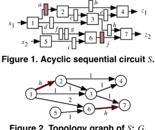
Figure 1. Acyclic sequential circuit S.
1 2
3 4
5 6
7 1 1 1 1
1 h h
2 1
Figure 2. Topology graph of S: G.
Example 1: Consider a sequential circuit S illustrated in Fig. 1. In this figure, 1, 2, . . . , 7 are logic blocks, b, c, . . . , i are L-registers, and a and j, which are highlighted, are H-registers. The topology graph G of this circuit S is shown in Fig. 2. ✷ 2.2 Time-Expansion Model (TEM)
A time-expansion model for an acyclic sequential circuit is de- fined based on the following time-expansion graph.
Definition 2 (Time-expansion graph (TEG)): Let S be an acyclic sequential circuit and let G= (V, A, r) be the topology graph of S. Let E = (VE,AE,t, l) be a directed graph, where VE is a set of vertices, AE is a set of arcs, t is a mapping from VE to a set of integers, and l is a mapping from VE to the set of vertices V in G. If graph E satisfies the following five conditions, graph E is said to be a time-expansion graph (TEG) of G.
C1(Logic preservation) The mapping l is a surjective, i.e.,
∀v ∈ V, ∃u ∈ VEs.t. v= l(u).
C2(Input preservation) Let u be a vertex in E. For any direct predecessor v(∈ pre(l(u))) of u in G, there exists a vertex u′in E such that l(u′) = v and u′∈ pre(u). Here, pre(v) denotes the set of direct predecessors of v.
C3(Time consistency) For any arc (u, v) (∈ AE), there exists an arc (l(u), l(v)) such that r(l(u),l(v)) = t(v) − t(u) or r(l(u),l(v)) = h.
C4(Time uniqueness) For any vertices u, v(∈ VE), if t(u) = t(v) and if l(u) = l(v), then the vertices u and v are identical, i.e., u= v.
C5(Hold consistency) For any pair of arcs (u1,v1), (u2,v2) (∈ AE) such that (l(u1),l(v1)) = (l(u2), l(v2)) and r(l(u1), l(v1)) = r(l(u2), l(v2)) = h, if t(u1) > t(u2), then t(u1) ≥ t(v2).
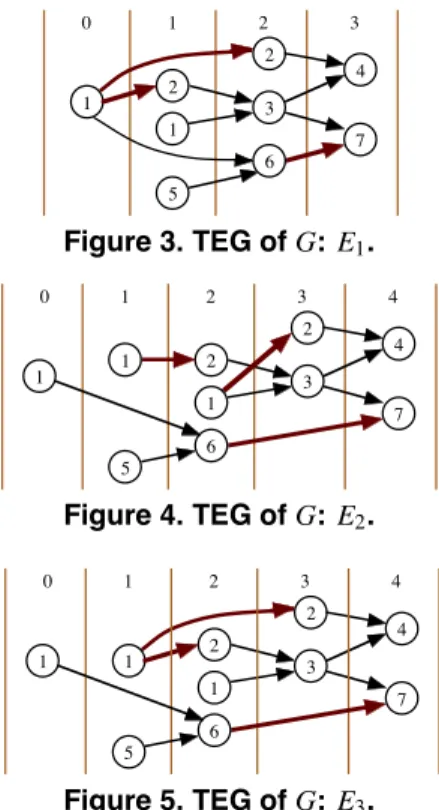
✷ This definition is written by adding the last condition C5 to that of the time-expansion graph for an acyclic sequential circuits without H-registers [11]. The condition C5 denotes that an H- register cannot read a new value while retaining a previous one. Example 2: Figs. 3, 4 and 5 show TEGs of topology graph G. In these figures, the number denoted in a vertex u is the label l(u), and the number located at the top of each column denotes the value of the labels t(u) of the vertices u in the column. ✷ quential circuits by supposing existence of a combinational logic block consisting only of lines or buffers between the two logic blocks.
1 2 3
4
5 6
7 1
1 2
2 3
0
Figure 3. TEG of G: E1.
2 3
4
5 6
7 1
1 2
2 3
0 4
1 1
Figure 4. TEG of G: E2.
1 2 3 2 4 1
5 6
7 1
1
2 3
0 4
Figure 5. TEG of G: E3.
As shown in the above example, there exist different TEGs for a topology graph according to control input sequences.
Definition 3 (Time-expansion model (TEM)): Let S be an acyclic sequential circuit, let G= (V, A, r) be the topology graph of S, and let E= (VE,AE,t, l) be a TEG of G. The combinational circuit CE(S) obtained by the following procedure is said to be the time-expansion model (TEM)of S based on E.
(1) For each vertex u ∈ VE, let logic block l(u) (∈ V ) be the logic block corresponding to u.
(2) For each arc(u, v) ∈ AE, connect the output of u to the in- put of v with a bus in the same way as(l(u),l(v)) (∈ A). Note that the connection corresponding to(u, v) has no reg- ister even if the connection corresponding to(l(u),l(v)) has a register (i.e., r(l(u), l(v)) ̸= 0).
(3) In each logic block, lines and logics that are reachable to neither other logic blocks nor primary outputs are removed.
✷ Example 3: Fig. 6 shows the TEM of sequential circuit S (Fig. 1) based on TEG E1(Fig. 3). In this figure, a highlighted part in a logic block represents a portion of the lines and gates removed by
Step (3) in Def. 3. ✷
2.3 Test Generation with TEM
Here we consider the relationship between input/output se- quences of an acyclic sequential circuit and input/output pat- terns of its TEM. Let S be an acyclic sequential circuit, and let G= (V, A, r) be the topology graph of S. Let E = (VE,AE,t, l) be a TEG of G, let CE(S) be the TEM of S based on E, and let tminbe the minimum of labels t in CE(S). An input pattern for CE(S) can be transformed into an input sequence for circuit S by the following procedure τS.
x10
x2
2 2 1
5 6
7 4 3 1
x11
z1 z2
Figure 6. TEM of S based on E1: CE1(S). Table 1. Input and output sequences for S ob- tained by transformation procedure τS.
Time 0 1 2 3
x1 I10 I11 X X
Data Input
x2 X I2 X X
Reg. a L H X X
Control Input
Reg. j X X L X
z1 X X X O1
Output
z2 X X X O2
Definition 4 (Transformation procedureτS):
(1) Control input sequence IH. Let IH(v′,v,t) denote an input value which is applied to an H-register(v′,v) (∈ A) at time t. For each arc(u′,u) ∈ AEsuch that r(l(u′), l(u)) = h, let
IH(l(u′),l(u),t − tmin)
=
! L(LOAD mode) (t = t(u′))
H(HOLD mode) (t(u′) + 1 ≤ t ≤ t(u) − 1) Let the values IH(v′,v,t) which are not defined by the above equation be X (don’t care).
(2) Data input sequence IS. For each logic block u ∈ VE in CE(S), let
IS(l(u),t(u) − tmin) = IC(u),
where IS(v,t) denotes an input-pattern applied to logic block vin S at time t, and IC(u) denotes an input-pattern applied to logic block u in CE(S).
✷ Note that in the above procedure, a control input sequence is obtained only from a TEG E independent of an input-pattern for TEM CE(S).
Lemma 1: Let ICbe an arbitrary input-pattern for TEM CE(S), and let IS and IH be a data input sequence and a control input sequence obtained by τS, respectively. The output pattern OC(u) obtained from a logic block u ∈ VEby applying input pattern ICto CE(S) is equal to the output pattern OS(l(u),t(u) − tmin) obtained from the corresponding logic block l(u) at time t(u) − tminby ap- plying data input sequence ISwith control input sequence IH. ✷
Example 4: Consider a TEM CE1(S) (Fig. 6) of a sequen- tial circuit S shown in Fig. 1. Suppose an input-pattern IC= (x10,x11,x2) = (I10,I11,I2) applied to CE1(S) and the correspond- ing output-pattern is OC= (z1,z2) = (O1,O2). According to the labels t in TEG E1(Fig. 3), the patterns ICand OCare transformed into the sequences shown in Table 1 by procedure τS. Here, X de-
notes a don’t-care value. ✷
Note that the length of the sequence obtained from a pat- tern for TEM CE(S) by procedure τS becomes maxu∈VE{t(u)} − minu∈VE{t(u)} + 1.
Let ISand IHbe a data input sequence and a control input se- quence for acyclic sequential circuit S such that the sequences de- termine the output pattern OS(v,t) of a logic block v (∈ V ) in S at time t, respectively. Here, a pattern that does not affect OS(v,t) in the input sequences ISand IH is considered as don’t-care. Input sequences ISand IH for S can be transformed into a TEG E and an input-pattern ICfor the TEM CE(S) by the following procedure τC.
Definition 5 (Transformation procedureτC):
(1) TEG E. Construct a TEG E= (VE,AE,t, l) in which there ex- ists a vertex u ∈ VEthat satisfies the following conditions. (1) l(u) = v ∧ t(u) = t, and
(2) For the control input value IH(v1,v2,t′) applied to an H- register(v1,v2) (r(v1,v2) = h) at time t′,
if IH(v1,v2,t′) = L, then there exists a vertex u1∈ Pre(u) such that l(u1) = v1∧ t(u1) = t′,
if IH(v1,v2,t′) = H, then there exists an arc (u1,u2) (∈ AE) such that u1,u2∈ Pre(u) ∧ t(u1) < t′∧ t(u2) > t′. Here, Pre(u) denotes the set of all predecessors of u.
(2) Input-pattern IC. For every input pattern IS(v′,t′) applied to each logic block v′ at time t′, if IS(v′,t′) affects output OS(v,t), then for the logic block u′that satisfies u′∈ l−1(v′) and t(u′) = t′, let IC(u′) = IS(v′,t′).
✷ Lemma 2: Let v (∈ V ) be an arbitrary logic block in acyclic sequential circuit S, and let IS and IH be a data input sequence and a control input sequence that are required to set the output of vto a pattern OS(v,t) at time t, respectively. Let E and ICbe a TEM and an input-pattern obtained from ISand IH by procedure τC, respectively. Let u(∈ VE) be the logic block that corresponds to v by the first step (1) in procedure τC. The output pattern OC(u) obtained from the logic block u by applying the input pattern ICto TEM CE(S) is equal to the output pattern OS(v,t). ✷
Note that as shown in the above procedure τC, a TEG (or TEM) is obtained from a control input sequence applied to H-registers in a sequential circuit, independent of data input sequences.
Next, let us consider the relationship between faults in an acyclic sequential circuit and those in its TEMs. Here we con- sider single stuck-at faults only in logic blocks as those in an orig- inal sequential circuit. The stuck-at faults on lines between logic blocks and in registers can be considered to be equivalent to those on input/output lines of logic blocks.
Definition 6 (Fault in TEM): Let S be an acyclic sequential circuit. Let G= (V, A, r) be the topology graph of S, let E = (VE,AE,t, l) be a TEG of G, and let CE(S) be the TEM of S based on E. Let F be the set of faults in S, and let FEbe the set of faults in CE(S). Suppose a fault f ∈ F in a logic block u in circuit S. Let fe∈ FEbe the fault corresponding to fault f . Fault feis a multiple fault that consists of all the faults existing on the same line in ev- ery logic block u ∈ l−1(v). That is, if the number of logic blocks usuch that l(u) = v is just one, then the fault feis a single fault,
otherwise, feis a multiple fault. ✷
From the above discussion, we have the following theorem.
x10 x2
2 2 1
5 6
7 4 1 3
x11
z1 1 x12 z2
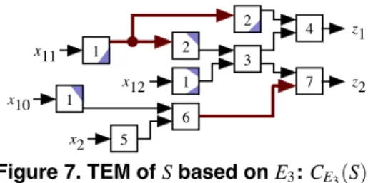
Figure 7. TEM of S based on E3: CE3(S). Theorem 1: Let S be an acyclic sequential circuit, and let F be the set of faults in S. Let G= (V, A, r) be the topology graph of S.
(1) A fault f ∈ F is testable (or irredundant) in S if and only if there exists a TEG E of G such that the fault fe(∈ FE) corresponding to f is testable in the TEM CE(S) based on E. (2) A test pattern for a fault fe(∈ FE) obtained using a TEM CE(S) can be transformed into a test sequence for the fault
f(∈ F) corresponding to fault fe.
✷ From this theorem, we can see that test generation for an acyclic sequential circuit can be performed by using several dif- ferent TEMs. Furthermore, since TEMs are fully combinational, a combinational test generator can be used for the test generation provided that the test generator can deal with multiple faults.
3 Cover Relation
From Theorem 1, we can have the following corollary. Corollary 1: Let S be an acyclic sequential circuit. Let F be a set of faults in S. A fault f ∈ F is untestable (or redundant) in S if and only if the fault corresponding to feis untestable in every TEM for
S. ✷
This corollary may imply that if a fault is untestable in an acyclic sequential circuit, in order to identify it, we must apply test generation to all the TEMs of the circuit, and identify the cor- responding fault as untestable in every TEMs. However, as men- tioned in the following discussion, all TEMs are not necessary for each identifying untestable fault.
Let us consider two TEMs CE1(S) (Fig. 6) and CE3(S) (Fig. 7) for sequential circuit S (Fig. 1). Suppose, in CE1(S), an output- pattern O2obtained from primary output z2by applying an input- pattern(Ia,Ib,Ic) to primary inputs (x10,x11,x2). This input/output relationship can be simulated by another TEM CE3(S) (Fig. 7) with four primary inputs x10, x11, x12and x2: by applying an input- pattern(Ia,Ia,Ib,Ic) to (x10,x11,x12,x2), the same output-pattern O2is obtained from z2in CE3(S). For such a relationship between two TEMs, we say CE3(S) covers CE1(S), and define it as follows. Definition 7 (Cover relation): Let S be an acyclic sequential circuit. Let G= (V, A, r) be the topology graph of S, and let E1= (V1,A1,t1,l1) and E2= (V2,A2,t2,l2) be arbitrary TEGs of G. TEG E1is said to cover TEG E2 if, for any vertex v2∈ V2, there exists a vertex v1∈ V1which satisfies the following two con- ditions, and it is denoted by E1- E2.
(1) l(v1) = l(v2), and
(2) for any pair of u1∈ Pre(v1) and u2∈ Pre(v2), if l1(u1) = l2(u2) and LE1(u1,v1) ∩ LE2(u2,v2) ̸= φ, then LE1(u1,v1) ⊆ LE2(u2,v2).
Here Pre(v) denotes the set of all predecessors of v and LE(u, v) denotes the set of paths(l(u), ..., l(v)) (in G) corresponding to paths(u, ..., v) whose tail and head are u and v in E, respectively.
✷ Example 5: Consider TEGs E1(Fig. 3) and E3(Fig. 5). Here, let abdenote a vertex v such that l(v) = a and t(v) = b. Sup- pose a pair of vertices 10and 73in TEG E1. There are two paths between 10 and 73: LE1(10,73) = {(1,2,3, 7), (1,6, 7)}. In the other TEG E3, vertex 74corresponds to vertex 73in E1uniquely, and there are two vertices u3 that satisfy lE3(u3) = lE1(10) and LE3(u3,74) ∩ LE1(10,73) ̸= φ: vertices 10and 11. LE3(10,74) = {1, 6,7} ⊆ LE1(10,73) and LE3(11,74) = {1,2, 3, 7} ⊆ LE1(10,73). By checking such a relationship as mentioned above, we can see that E3covers E1. Note that E1does not cover E3. ✷
When a TEG E1 covers a TEG E2, we denote that E1- E2. Further, it is also said that TEM CE1(S) covers TEM CE2(S)
(CE1(S) - CE2(S)).
Let IE2 be an input-pattern for TEM CE2(S) (covered by TEM CE1(S)) such that the pattern determines the output-pattern OE2(v2) of a logic block v2 (∈ V2). Based on Def. 7, input- pattern IE2can be transformed into an input-pattern IE1for TEM
CE1(S) (- CE2(S)) by the following procedure τR.
Definition 8 (Transformation procedure τR): Let v1 (∈ V1) be a logic block corresponding to v2 that satisfies the condi- tions in Def. 7. Let IE2(u2) denote an input-pattern applied to a logic block u2 (∈ Pre(v2) ∪ {v2}). For every logic block u1 (∈ Pre(v1) ∪ {v1}) corresponding to u2(l1(u1) = l2(u2) and LE1(u1,v1) ∩ LE2(u2,v2) ̸= φ), let IE1(u1) = IE2(u2). Note that the number of logic blocks u1corresponding to one logic block u2is
one or more. ✷
Lemma 3: Suppose two TEMs C1and C2of an acyclic sequential circuit such that C1- C2. Let v2be an arbitrary logic block in C2. Let I2be an input-pattern required to set the output of v2to a pattern O2. Let I1be an input-pattern obtained by procedure τR
from I2. The output-pattern O1obtained from v1corresponding to v2by applying the input-pattern I1to C1is equal to the output-
pattern O2. ✷
As mentioned above, if a TEM C1 covers another TEM C2, C1can ‘simulate’ C2.On the other hand, by definition Def. 6, for any fault in an acyclic sequential circuit, the corresponding fault is defined in either TEM of C1 and C2. Thus, we can form the following theorem.
Theorem 2: Let S be an acyclic sequential circuit. Let C1 and C2be TEMs of S. Let F1and F2be the set of faults in C1and C2, respectively (Def. 6). If TEM C1covers TEM C2, the following holds: If a fault f2(∈ F2) in C2is testable, fault f1(∈ F1) in C1
corresponding to f2is also testable. ✷
From the theorem, we can see that test generation for all the TEMs that are not covered by any other TEMs, i.e., maximal TEMs of an acyclic sequential circuit is necessary and sufficient to obtain a complete test sequence for all testable faults in the cir- cuit. For example, sequential circuit S has two maximal TEMs CE2(S) and CE3(S), i.e., any TEM is covered by either CE2(S) or CE3(S).
1 2
4
3
5 6
1 1
1 h 1
1
h 2
3
(a) Topology graph: Gm.
0 1 2 3 4 5 6 7
1 2
4
3
5 6
1 4
1
2 1 4
1
(b) Time-expansion model of Gm: Em. Figure 8. Example of max-testable circuit. Thus, we can reduce the number of TEMs for complete test generation of sequential circuits, even though the number of con- trol sequences for H-registers is unlimited.
4 Max-testable structure
In general, an acyclic sequential circuit has several maximal TEMs, e.g., the maximal TEMs of sequential circuit S (Fig. 1) are CE2(S) and CE3(S). However, if the number of maximal TEMs is just one for an acyclic sequential circuit i.e., the circuit has the maximumTEM, a complete test set for the circuit can be gen- erated only by performing combinational test generation for the maximum TEM. If a sequential circuit has the maximum TEM, the sequential circuit is called max-testable.
4.1 Path-Adjustable Structure
Consider sequential circuit S (Fig. 1), again. Recall that TEG E3(Fig.5) covers another TEG E1(Fig. 3). Focus on an arc(6, 7) which corresponds to an H-register j (called hold arc, for short) in S, we can consider that TEG E3is obtained from E1by adjusting the length of the arc(6, 7) (i.e., the difference of t(6) and t(7)) so that the tail 1 of a path(1,6, 7) is separated from that of another path(1, 2,3, 7) that has the same head 7. In this way, if a common tail of different paths that have the common head can be divided into distinct vertices as respective tails of the paths under Condi- tion C5 in Def. 2, another TEG covering the original TEG can be obtained.
Here, as a sufficient condition for the maximum TEM, we have the following lemma.
Lemma 4: Let G= (V, A, r) be the topology graph of an acyclic sequential circuit S. Let E= (VE,AE,t, l) be a TEG for G. A TEG is maximum if for any pair of vertices u, v ∈ VE, the following holds.
∀p, q ∈ PE(u,v)[HE(p) = HE(q)],
where PE(u, v) denotes the set of paths whose head and tail are uand v in E, respectively, and HE(p) denotes the set of hold arcs(u′,v′), such that the corresponding arc (l(u′),l(v′)) is an H- register (i.e.,(l(u′), l(v′)) = h) on path p. ✷
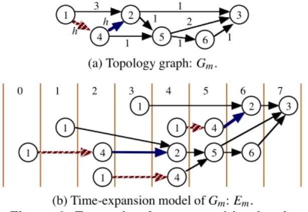
Example 6: Consider a TEG Emfor a topology graph Gm(Fig. 8). For any pair of paths p, q whose tail and head are severally the same in Em, the set HEm(p) of hold arcs is equal to that HEm(q).
Hence, TEG Em is the maximum, and consequently the circuit represented by topology graph Gmis max-testable. ✷
x1 1 z1 2
3
4
5 6
a b
c
d
e f
g i
h
Figure 9. Sequential circuit S2.
Although TEG Em shown in the above example is the max- imum, it seems to be hard to derive the maximum TEG for G because adjustability of each hold arc depends on resultant ad- justment of the other hold arc. From the practical point of view, an acyclic sequential circuit whose maximum TEG (TEM) can be derived easily is interesting and important. Here, recall that Con- dition C5 in Def. 2 is for more than one hold arc that corresponds to a certain H-register in an acyclic sequential circuit. Such arc duplication for an H-register is possible in a TEG when there exist more than one paths from the H-register to an primary output in the circuit. Hence, here we consider a sequential circuit whose maxi- mum TEG can be derived by adjusting each hold arc independent of the others as follows.
Definition 9 (Path-adjustable structure): Let S be an acyclic sequential circuit. Let G= (V, A, r) be the topology graph of S. Let P(u,v) denote a set of paths from u to v (u,v ∈ V ). If G satisfies the following condition, sequential circuit S is said to be path- adjustable.
(CPA) Let V′(⊆ V ) be a set of vertices which are reachable from some arc ah(∈ A) such that r(ah) = h (H-register). Let u, v be any pair of vertices in V′. For any pair of paths p, q ∈ P(u, v), (1) if H(p) = H(q), then d(p) = d(q), else
(2) if H(p) ̸= H(q), then
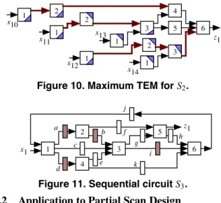
H(p) ∩ H(q) ̸= φ ⇒ H(p) ⊂ H(q) ∨ H(p) ⊃ H(q). Here d(p) denotes the sum of labels r(a) of arcs a (∈ A) such that r(a) ∈Z+(L-register) in a path p, and H(p) denotes the set of arcs a such that r(a) = h (H-register) in a path p. ✷ Example 7: Consider a sequential circuit S2 shown in Fig. 9. In this figure, a, b, d and i are H-registers, and the others are L- registers. For example, let us focus on an H-register a. There exist four paths to be considered for a: p1= (2, d,4, f , 6), p2= (2, b, 3,e, 4, f , 6), p3 = (2, b,3, g, 5, h, 6) and p4= (2, b, 3,i, 6). Then, H(p1) = {d}, H(p2) = {b},H(p3) = {b} and H(p4) = {b, i}. For p1and p2, H(p1) ∩ H(p2) = φ, this is in neither case. For p2 and p3, H(p2) = H(p3) = {b} and d(p2) = d(p3), i.e., case (1). For p2 and p4, H(p2) ⊂ H(p4), i.e., case (2). Sim- ilarly, all the other pairs of paths in this circuit S2 also satisfy Condition CPA, and hence S2 is path-adjustable. Note that a sequential circuit S (Fig. 1) is not path-adjustable. As a result, we can obtain the maximum TEM for S2 as shown in Fig. 10. The control input sequence obtained from the TEM (by procedure τS) is IH(a) = (L, L, L, H, X, X, X), IH(b) = (X, X,L, H, L, X, X), IH(d) = (X, L, H, H, H, X, X), IH(i) = (X, X, X, X, X, L, X). ✷
For a path-adjustable circuit, a TEG that satisfies the condition in Lemma 4. Therefore, we have the following theorem.
Theorem 3: A path-adjustable sequential circuit is max-testable.
✷
z1 x10
x11 x12
x13
x14
1 2
3 4
5 6
3 1 1 2 2
1 1
Figure 10. Maximum TEM for S2.
x1
z1 1
2
3 4
5 6
a b
c
d e
f g
i h j
k
Figure 11. Sequential circuit S3. 4.2 Application to Partial Scan Design
From Theorem 3, we can see that for any sequential circuit, by selecting a sufficient set of scan registers so that the resulting kernel is path-adjustable, a complete test sequence for the circuit can be obtained by using a combinational test generator for only the maximum TEM of the kernel (provided that the test generator can deal with multiple faults). On the other hand, from Def. 9, we have the following corollary.
Corollary 2: All the following sequential circuits are path- adjustable.
(1) balanced structures [5],
(2) internally-balanced structures [7], and
(3) acyclic sequential circuits without H-registers. ✷ Therefore, for a sequential circuit, the hardware overhead of the partial scan based on path-adjustable structure is smaller than that based on the structures mentioned in Corollary 2.
Example 8: Consider a sequential circuit S3 shown in Fig. 11. In this figure, a, b, d and i are H-registers, and the others are L-registers. In the partial scan design based on path-adjustable structure, the minimum number of scan registers is two, e.g., by scanning L-registers j and k, the resulting kernel becomes path- adjustable. Note that there is an alternative DFT solution: if one L-register j is scanned and another L-register k is replaced with an H-register, then the resultant circuit is also path-adjustable.
On the other hand, in the partial scan design based on balanced structure, the minimum number of scan registers is five, e.g., the set of registers to be scanned is{b,c,e, f , k}. When the kernel is made an acyclic structure without H-registers, the minimum num- ber of scan registers is also five, e.g.,{a, b, d,h, i}. ✷ Therefore, it is seen that we can obtain complete test sequences for sequential circuits with low hardware overhead based on max- testable structure.
5 Conclusions and Future Works
In this paper, we presented a method of test generation for acyclic sequential circuits with hold registers. A complete test set for an acyclic sequential circuit can be obtained by applying a com- binationaltest generator to all the maximal time-expansion models (TEMs)of the circuit. As a class of max-testable sequential cir-
cuits, referring to acyclic sequential circuits for which the number of maximal TEMs is one, i.e, the maximum TEM exists, we intro- duced path-adjustable structure. The class of path-adjustable se- quential circuits properly includes several known classes of acyclic sequential circuits such as balanced structures and acyclic sequen- tial circuits without hold registers for which test generation can be also performed by using a combinational test generator. There- fore, the hardware overhead for partial scan based on our path- adjustable structure is substantially smaller than that based on bal- anced or acyclic sequential structure without hold registers.
As future works, several issues are remaining.
• The condition in the definition of path-adjustable structure is a sufficient one for existence of the maximum TEM for acyclic sequential circuit. We believe that there exists a lager class of max-testable sequential circuits, and hence the hard- ware overhead of DFT for complete test sequences can be reduced further.
• We are now investigating an algorithm for finding an optimal partial scan / hold register insertion based on max-testable structure with minimum hardware overhead.
• The length of test sequences obtained from test generation using TEMs depends on the structure of the TEMs. Hence, it is also important to find optimal TEMs which minimize the length of resulting test sequences.
Acknowledgments
The authors would like to thank Drs. Toshimitsu Masuzawa Michiko Inoue and Satoshi Ohtake of Nara Institute of Science and Technology, Japan and Dr. Akio Tamura of Hiroshima City University, Japan for their fruitful comments and discussions.
References
[1] H. Fujiwara, Logic Testing and Design for Testability, The MIT Press, 1985.
[2] M. Abramovici, M.A. Breuer, and A.D. Friedman, Digital Systems Testing and Testable Design, Computer Science Press, 1990. [3] K.-T. Cheng and V.D. Agrawal, “A partial scan method for sequential
circuits with feedback,” IEEE Trans. Comput., Vol.39, No.4, pp.544– 548, Apr. 1990.
[4] D.H. Lee and S.M. Reddy, “On determining scan flip-flops in partial- scan design approach,” in Proc. Int. Conf. Computer-Aided Design, pp.322–325, Nov. 1990.
[5] R. Gupta, R. Gupta, and M.A. Breuer, “The BALLAST methodol- ogy for structured partial scan design,” IEEE Trans. Comput., Vol.39, No.4, pp.538–544, Apr. 1990.
[6] A. Balakrishnan and S.T. Chakradhar, “Sequential circuits with com- binational test generation complexity,” in Proc. Int. Conf. on VLSI Design, Jan. 1996, pp.111–117.
[7] T. Takasaki, T. Inoue, and H. Fujiwara, “Partial scan design methods based on internally balanced structure,” in Proc. Asia & South Pacific Design Automation Conf., 1998, pp.211–216.
[8] R. Gupta and M.A. Breuer, “Partial scan design of register-transfer level circuits,” Journal of Electronic Testing: Theory and Applica- tions, Vol.7, pp.25–46, 1995.
[9] A. Kunzmann and H.-J. Wunderlich, “An analytical approach to the partial scan problem,” Journal of Electronic Testing: Theory and Ap- plications, Vol.1, pp.163-174, 1990.
[10] R. Gupta and M.A. Breuer, “Testability properties of acyclic struc- tures and applications to partial scan design,” in Proc. IEEE VLSI Test Symp., 1992, pp.49–54.
[11] Tomoo Inoue, Toshinori Hosokawa, Takahiro Mihara, and Hideo Fu- jiwara, “An optimal time expansion model based on combinational
test generation for RT level circuits,” in Proc. IEEE Asian Test Symp., 1998, pp.190-197.