A Reconfigurable Wrapper Design for Multi-Clock Domain Cores
Takashi Yoshida, Tomokazu Yoneda, Hideo Fujiwara
Graduate School of Information Science,Nara Institute of Science and Technology
8916-5 Takayama, Ikoma, Nara 630-0192,Japan
{ takashi-y, yoneda, fujiwara }@is.naist.jp
Abstract
This paper presents a method for designing reconfig- urable wrappers for cores with multiple clock domains to reduce test time. In the proposed method, we divide test application into two steps considering the difference of test data volume in inter-domain tests and intra-domain tests of multi-clock domain cores. The test time can be reduced by designing an optimal wrapper for each step and switch- ing them during the test application. Experimental results show the effectiveness of the proposed method compared to the previous wrapper designs for multi-clock domain cores. keywords SoC test, wrapper design, multi-clock domain core
1 Introduction
System-on-Chips (SoCs) embed a lot of Intellectual Property (IP) cores such as processors and memories, and enable us to design complex systems in a short period. In the core-based SoC test environment, cores are tested in a modular fashion [1]. A modular test requires an IEEE 1500 wrapper [2] per core and Test Access Mechanism (TAM). The design of wrapper and TAM has a great influence on the SoC test time. Therefore, a lot of methods have been proposed for wrapper and TAM design and optimization [3, 4, 5, 6, 7, 8].
However, today’s complex IP cores operate at multi- ple clock frequencies internally. The wrapper designs for cores operating at single clock frequency cannot apply to the multi-clock domain cores because of the following rea- sons: (1) the clock skew problem during test should be considered, (2) all the inter-domain and intra-domain data transfers should be tested at-speed.
A few approaches have been proposed for the wrapper design of multi-clock domain cores [9, 10, 11, 12]. In [9, 10], the core was divided into its clock domains called virtual core and single frequency wrapper was designed for each virtual core to avoid the clock skew during shift op- eration. Moreover, by designing at-speed capture window proposed in [13], they achieved the at-speed test of all the inter-domain and intra-domain data transfers without clock skew during capture operation. In [11, 12], the authors uti-
lized gated-clocks to allow a more flexible and efficient test scheduling during shift operation under a power constraint. This paper presents a design and optimization method of wrappers for multi-clock domain cores to further reduce the test time. In multi-clock domain cores, we have to con- sider two kinds of tests: (1) intra-domain tests and (2) inter- domain tests, and the test data volume as well as the neces- sary FFs are different for each test. However, all the pre- vious works didn’t consider the difference and presented methods to minimize the scan shift time for one test pattern. On the other hand, we focus on the difference of the test data volume as well as the necessary FFs, and present a method to minimize the overall test time. The proposed method divides test application into two steps and designs an opti- mal wrapper for each step. The test time can be reduced by switching the wrapper configurations during the test appli- cation. Experimental results show the effectiveness of the proposed method compared to the previous wrapper designs for multi-clock domain cores.
The rest of this paper is organized as follows. The pre- vious work and motivation for this work are discussed in Section 2. Section 3 describes the proposed wrapper design method. Section 4 presents experimental results and com- parisons with previous work. Finally, Section 5 concludes this paper.
2 Previous Work and Motivation
The wrapper designs for multi-clock domain cores have been proposed in [9, 10, 11, 12]. An example of the wrapper design proposed in [10] is shown in Figure 1.
In all the previous approaches, the core was divided into its clock domains called virtual core (VC), and single fre- quency wrapper design was performed on each VC to as- sign a virtual core wrapper (VCW). By forming wrapper scan chains within the same clock domain, they eliminated the clock skew problem during shift. Each VCW is con- nected to the core interface through internal virtual test bus (VTB) lines. Clock signals (Gated clk) and scan enable sig- nals (Scan en) were provided by the Scan Control Block. Each VCW can operate at a distinct shift frequency and the number of internal VTB lines is not necessarily the same 9th IEEE Workshop on RTL and High Level Testing (WRTLT'08), pp. 13-18, Nov. 2008.
VC1
VC2 Scan Chain A2
Scan Chain B1 Scan Chain B2 Scan Chain B3 Scan Chain A1
TAM-In
VTB VTB
TAM-Out VCW1
VCW2
TCK(clk1) clk2
seld selm
VC3 Scan Chain C
VCW3
VTB-DIU VTB-MIU
clk3
Scan Control Block Gated_clk[1...3] Scan_en[1...3]
Figure 1. Multi clock domain core wrapper.
intra-domain test inter-domain test
Gated_clk[1] TCK
Gated_clk[2] Scan_en[1]
Scan_en[2]
Capture Window
Gated_clk[3] Scan_en[3]
intra-domain test inter-domain test intra-domain test inter-domain test
Gated_clk[1] TCK
Gated_clk[2] Scan_en[1]
Scan_en[2]
Capture Window
Gated_clk[3] Scan_en[3]
Figure 2. Timing diagram.
as the external TAM width provided to the core. By intro- ducing VTB de-multiplexing interface unit (VTB-DIU) and VTB multiplexing interface unit (VTB-MIU), each VCW i can have V T Bi internal VTB lines operating at shift fre- quency fithat satisfies Wext×ft≥!V T Bi×fi, where Wextis the external TAM width assigned to the core and ft
is the tester frequency.
Moreover, by designing the at-speed capture window proposed in [13], they achieved at-speed test of all the inter- domain and intra-domain data transfers without clock skew during capture operation. Figure 2 shows a timing diagram of the test application. In the capture window, at-speed clock and scan enable signal for each domain are provided by the scan control block. In Figure 2, three intra-domain tests and six inter-domain tests are performed in the capture window.
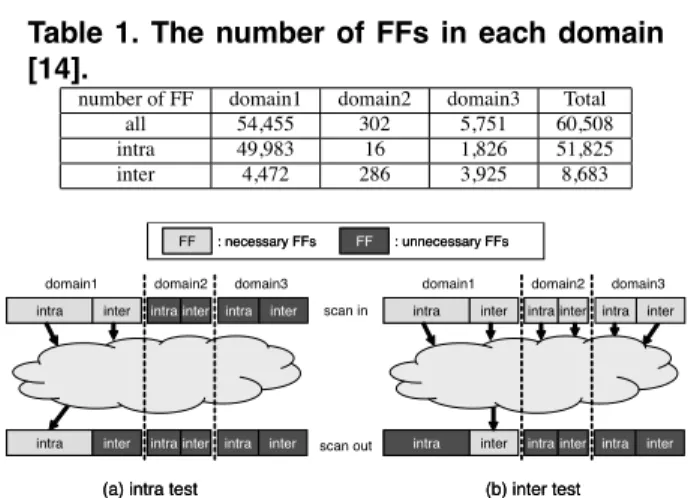
However, those tests target the different part of the cir- cuit, and they differ from each other in terms of test the data volume. Table 1 shows the number of FFs in the multi-clock domain circuit used in [14]. “all” denotes the number of FFs that belong to the clock domain. “inter” and “intra” de- note the number of FFs that receive data transfers from FFs in other domains and the number of FFs that receive data transfers only from FFs in the same domain, respectively.
For a intra-domain test (i.e., the test of intra-domain data transfers within a domain), all FFs in the domain are re- quired to scan in while only the intra-FFs in the domain are required to scan out (Figure 3(a)). On the other hand, for a
Table 1. The number of FFs in each domain [14].
number of FF domain1 domain2 domain3 Total
all 54,455 302 5,751 60,508
intra 49,983 16 1,826 51,825
inter 4,472 286 3,925 8,683
(a) intra test (b) inter test
(a) intra test (b) inter test
intra inter
intra inter intra interintra inter intra inter
intra inter
intra inter intra interintra inter intra inter
domain1 domain2 domain3
intra inter
intra inter intra interintra inter intra inter
intra inter
intra inter intra interintra inter intra inter
domain1 domain2 domain3
scan in
scan out
FF : necessary FFs FFFF : unnecessary FFs FF : necessary FFs : unnecessary FFs
Figure 3. Necessary FFs for inter/intra do- main tests of domain 1.
inter-domain test (i.e., the test of inter-domain data transfers from a domain to another domain), all FFs in all domains are required to scan in while only inter-FFs in the domain are required to scan out (Figure 3(b)). Assuming that test data volume for each test is proportional to the number of FFs related to the test, we can observe from Table 1 that the test data volume of intra-domain tests is larger than that of inter-domain tests. Moreover, intra-domain tests differ from each other in terms of the test data volume.
All the previous works for the multi-clock domain cores proposed methods to minimize the shift time for one test pattern assuming that all the FFs are always required to scan in and out. However, as shown in above, the intra-domain tests and inter-domain tests differ from each other in terms of the test data volume and necessary FFs. Consequently, at some point during the test application, the tests with small test data volume will be completed and some FFs might be- come unnecessary for the remaining tests. Especially, af- ter all the inter-domain tests are finished, all the inter-FFs are not required to scan out for the remaining intra-domain tests. Moreover, it is not necessary to synchronize with the capture window since each intra-domain test is independent from others. From the above observation, we conclude that the difference in the test data volume as well as necessary FFs should be considered for effective wrapper design for mutli-clock domain cores.
3 Proposed Wrapper Optimization
3.1 Overview
In this section, we present an efficient wrapper design method which considers the difference in the test data vol- ume as well as necessary FFs for each intra and inter test in multi-clock domain cores. The basic strategy of the proposed method is to utilize the reconfigurable wrapper proposed in [5]. Theoretically, the overall test time can
(a) Step 1 (b) Step 2
(a) Step 1 (b) Step 2
intra inter
intra inter intra interintra inter intra inter
domain1 domain2 domain3
intra inter
intra inter intra interintra inter intra inter
intra inter
intra inter intra interintra inter intra inter
domain1 domain2 domain3
scan in
scan out FF
FF : necessary FFs FF : unnecessary FFs FF : necessary FFs : unnecessary FFs
intra inter
intra inter intra interintra inter intra inter
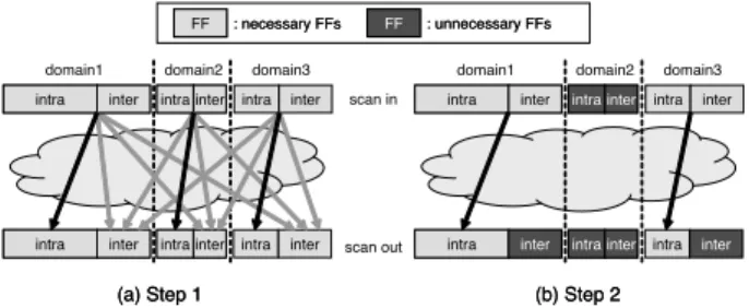
Figure 4. Proposed 2-step test application.
be minimized by designing a reconfigurable wrapper that can switch its configuration whenever the necessary FFs are changed during test application. However, there is a trade- off relation between the test time and the area overhead for wrapper reconfiguration. Therefore, in the proposed method, we divide the test application into two steps, and design a distinct optimal wrapper for each step to reduce the overall test time. For each step, the proposed method uses the same wrapper architecture proposed in [10] shown in Figure 1 as its basis.
In Step 1, we perform the intra-domain tests and inter- domain tests simultaneously as shown in Figure 4(a). For this step, we use the same wrapper design method as [10] where the objective is to minimize the shift time for one test pattern and all FFs in all domains are required to both scan in and out. In Step 1, we apply tests using this wrapper configuration repeatedly until all the inter-domain tests are finished.
In Step 2, we perform the remaining intra-domain tests as shown in Figure 4(b). As we explained in Section 2, each intra-domain test is independent from others and it is not necessary to synchronize with the capture window. Fur- thermore, all the inter-FFs are not required to scan out. In Section 3.2, we first present an effective single frequency virtual core wrapper design for each domain where some FFs are not required to scan out. Then, Section 3.3 presents an wrapper optimization method for Step 2.
3.2 Single-Frequency Virtual Core Wrapper
In this paper, we assume that each scan chain is formed by either inter-FFs only or intra-FFs only. We define the scan chain that consists of inter-FFs only as “inter-SC”. Similarly, we define the scan chain that consists of intra- FFs only as “intra-SC”. Figure 5(a) shows an example of virtual core with two inter-SCs and one intra-SC. In Step 2, we only perform the intra-domain tests. Therefore, for each intra-domain test, both intra-SCs and inter-SCs in the domain are required to scan in while only intra-SCs are re- quired to scan out. Note that we can consider the scan chain that consists of both intra-FFs and inter-FFs by regarding it as “intra-SC”.
For each intra-domain test in Step 2, the test data vol- ume for scan in is larger than that for scan out since there
(a) core with intra-SCs and inter-SCs. intra:100
inter :80 inter :60
(b) Conventional wrapper.
no output
intra:100 inter :80 inter :60
(c) Proposed wrapper. intra:100 inter :80 inter :60 (a) core with intra-SCs and inter-SCs.
intra:100 inter :80 inter :60
(b) Conventional wrapper.
no output
intra:100 inter :80 inter :60
(c) Proposed wrapper. intra:100 inter :80 inter :60
Figure 5. Comparison of wrapper configura- tions
exist inter-SCs. Therefore, in the proposed single frequency virtual core wrapper design, we use the different number of wrapper pins for scan in and out. In the conventional wrap- per designs proposed in [3, 6], each wrapper scan chain needs two wrapper pins. Figure 5(b) shows an example of the conventional wrapper design with two wrapper scan chains which is mapped to four wrapper pins. Let si(so) be the length of the longest wrapper scan-in (scan-out) chain. Then, in Figure 5(b), siand soare equal to 140 and 101, re- spectively. The test time (TAT) is 14101 cycles by Equation (1) when we assume the number of test pattern p is 100.
T AT = (max(si, so) + 1) × p + min(si, so) (1) On the other hand, the proposed method uses three wrap- per pins for scan in and one wrapper pin for scan out as shown in Figure 5(c). Consequently, the proposed wrapper consists of one wrapper scan chain which can be scanned in and out, and two wrapper scan chains which can be scanned in only. In this example, si, soand T AT are equal to 100, 101 and 10200, respectively, and we can reduce the test time by 27% compared to the conventional wrapper shown in Figure 5(b).
In the single frequency virtual core wrapper design for Step 2, the partitioning of wrapper pins for scan in and out as well as the assignment of scan chains to the wrapper pins greatly affect the test time. Then, we formally present the single frequency virtual core wrapper design problem Pvcw
as follows.
Definition 1 Pvcw: Given the number of wrapper pins Wvc
and the test parameters for a virtual core VC including
• Nin: number of primary inputs
• Nout: number of primary outputs
• Nbi: number of bidirectional I/Os
• Nsc: number of scan chains for each scan chain i(1 ≤ i ≤ Nsc)
Algorithm VirtualCoreWrapperDesign(Wvc, V C) 1: Wo=1, Tmin=∞
2: while Wo≤ Wvc2 do
3: Nio= Wo, Ni= Wvc−2Wo
4: Create Nioio-wrapper scan chains Rio,and Niin-wrapper scan chain Rin
5: // Part(i)
6: Sort intra-SC∈ V C in descending order of length 7: for each intra-SC i do
8: Find the longest wrapper scan chain rmaxin Rio
9: Find the shortest wrapper scan chain rminin Rio
10: Assign i to wrapper scan chain r
11: such that length(rmax)-(length(r)+li) is minimum 12: if there is no such wrapper scan chain r then 13: Assign i to rmin
14: end if
15: end for 16: // Part(ii)
17: Repeat steps 5 through 13 to add the inter-SC∈VC to Rio∪Rin
18: // Part(iii)
19: Repeat steps 5 through 13 to add the bidirectional I/Os∈VC to Rio
20: // Part(iv)
21: Repeat steps 5 through 13 to add the primary inputs∈VC to Rio∪Rin
22: // Part(v)
23: Repeat steps 5 through 13 to add the primary outputs∈VC to Rio
24: Calculate Tcurfor current virtual wrapper configuration by Equation (1) 25: if Tmin> Tcurthen
26: Record current virtual wrapper configuration to V CW 27: Tmin= Tcur
28: end if 29: end while 30: return V CW
Figure 6. Pseudocode for Virtual Core Wrap- per Design
– li: length
– typei: type (inter-SC or intra-SC)
• p: number of test patterns
determine the virtual core wrapper VCW for VC such that the TAT defined by Equation (1) is minimized.
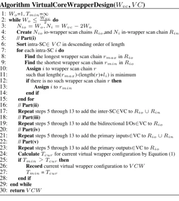
The proposed algorithm for Pvcw is shown in Figure 6. First, we initialize the number of wrapper output pins Wo=1 and the minimum test time Tmin=∞ (line 1). Then, the al- gorithm repeats the procedure from line 2 to 29 until Woex- ceeds W2vc. From line 3 to 4, we create Nio(= Wo) empty wrapper scan chains with wrapper pins for both scan in and out called io-wrapper scan chains, and Ni empty wrapper scan chains with wrapper pin for scan in only called in- wrapper scan chains. From line 6 to 15, we assign intra- SCs to the set of io-wrapper scan chains Rio. We adopt the same strategy as Design wrapper procedure proposed in [6] for the assignment. Similarly, inter-SCs, bidirectional wrapper cells, input wrapper cells and output wrapper cells are assigned to the set of wrapper scan chains (line 16-23). The main difference from Design wrapper is that intra-SCs, bidirectional wrapper cells, and output wrapper cells can be assigned only to Rio. This process is repeated for all the possible partitioning for wrapper pins, and find a solution with the shortest test time.
3.3 Multi-Frequency Wrapper Design
In this section, we present a multi-frequency wrapper design for Step 2 explained in Section 3.1. The problem
we examine in this section is to minimize the test time in Step 2 by determining the test start time, the shift frequency and the single frequency wrapper design for every domain under a power constraint. Before describing the proposed solution, we formally present the multi-frequency wrapper design problem Pwas follows.
Definition 2 Pw: For a core C, given
• ft: ATE shift frequency
• Wext: number of external test pins
• Pmax: maximum power consumption
• F = {F1, . . . , FM|Fk+1= F2k, k ∈1, . . . , M − 1} : set of allowed shift frequencies
• Nd: number of clock domains for each clock domain i (1 ≤ i ≤ Nd)
– V Ci: virtual core
– Pi: power consumption at frequency F1
determine the wrapper design for the core C including for each clock domain i
• Wi: number of wrapper pins
• ti: test start time
• fsi: shift frequency under the following constraints:
• the power consumption at any time cannot exceed the maximum power consumption Pmax,
• the internal bandwidth at any time cannot exceed the external bandwidth,
• the shift frequency fsishould belong to the set of al- lowed shift frequencies F ,
such that the test time is minimized.
In this paper, we adopt the same test scheduling strategy proposed in [9, 10] where the test start time of every clock domain is fixed to time 0 (i.e., ti=0). In the next section, we present an integer linear programming (ILP) model for Pw
to derive an optimal solution.
3.4 ILP Model for Multi-Frequency Wrap-
per Design Problem
The shift frequencies fsi of each domain must be- long to the set of allowed shift frequencies F = {F1, . . . , FM|Fk+1 = F2k, k ∈ 1, . . . , M − 1}. Let Wi be the number of wrapper pins assigned to domain i. Then, the maximum value of Wiis Wmax=Fft
M×Wext−2 × (Nd−
1). We can pre-calculate T (i, j, k) which is the test time when Wi= j and fsi= Fkby using the method proposed in Section 3.2.
Next, let us define two binary variables as follows.
• δij: δij= 1 only if Wi = j.
• θik: θik= 1 only if fsi= Fk.
Then, Pwcan be represented as the following ILP model. Objective:
Minimize maxi{
W"max
j=1
"M k=1
δij× θik×T(i, j, k)}, i.e., the
overall test time in Step 2 is minimized. Subject to:
1.
W"max
j=1
δij = 1, 1 ≤ i ≤ Nd,i.e., every virtual core is assigned to exactly one number of wrapper pins for its wrapper design.
2.
"M k=1
θik = 1, 1 ≤ i ≤ Nd,i.e., every virtual core is shifted in exactly one frequency.
3.
Nd
"
i=1
"M k=1
θik×Pi×Fk F1
≤Pmax,i.e., the power con- sumption does not exceed the constraint.
4.
Nd
"
i=1
Wi×fsi≤Wext×ft,i.e., the internal scan band- width does not exceed the external bandwidth.. Wi,fsiare expressed as follows:
Wi=
W"max
j=1
δij×j (2)
fsi=
"M k=1
δik×Fk (3)
Constraint 4 can be expressed using Equation (2) and (3) as follows.
Nd
"
i=1 W"max
j=1
"M k=1
δij× θik×Fk×j ≤ Wext× ft FM
The non-linear term δijθik can be easily linearized. However, due to the limited space, we decided to omit it.
4 Experimental Results
We made experiments on the benchmark multi-clock do- main core hCADT01 used in [10,12,13]. As the original hCADT01 does not include the number of test patterns for each test and the type of scan chain (i.e., inter-SC or intra- SC), we have added those information. The information we used in our experiments for hCADT01 is shown in Table 2.
“intra-SC” and “inter-SC” denote the length of each scan chain which is classified into intra-SC and inter-SC, respec- tively. “Nintra,i” denotes the number of test patterns for intra-domain test for each domain. Let N1 be the number of test patterns applied in Step 1 (i.e., the maximum value of the number of all the inter-domain tests), and let N2,ibe the number of remaining test patterns for intra-domain test of domain i in Step 2. We assume that N1 is equal to 200 and N2,iis equal to Nintra,i−d×N1(i.e., for each domain, d × N1intra-domain test patterns are applied in Step 1). We also assume that the number of allowed shift frequencies (M ) is 4 and F1=ft=100 MHz.
Table 3 compares the test time of hCADT01 when dif- ferent values for d and different power constraints Pmax
are considered. Columns “T[10]” and “Tnew” denote the test time by [10] and the proposed method, respectively.
“∆T ” is the relative difference between T[10] and Tnew. We used a public ILP solver lp solve [reference] and all the experimental results were obtained less than 1 minute on a PC with AMD Opteron256 3.0GHz and 16GB memory. The proposed method can obtain savings in test time up to 40.56% and 27.45% saving on average. This is because [10] uses one wrapper configuration through the test application while the proposed method can switch it to the optimal con- figuration for Step 2. In some cases for Pmax=1500 and 3000, the test time is increased by 0.09%. For those cases, [10] and the proposed method achieved the same test time for each step. However, the last scan out of Step 1 and the first scan in of Step 2 cannot be overlapped in the proposed method because of the wrapper reconfiguration, and it in- curred the 0.09% increase for those cases.
In [9, 10], the hardware overhead of the scan control block was stated to be less than 10% of the size of the ex- isting IEEE 1500 wrapper and scan logic. Additionally, the proposed method requires the hardware for the wrapper re- configuration. However, even in the worst case, a slight modification of the scan control block and only one mul- tiplexer per scan element (i.e., scan chain or wrapper cell) are required for the reconfiguration. This is insignificant for complex and large IP cores.
In this paper, we adopted the method proposed in [10] for Step 1 and compared the proposed method only with [10]. However, the proposed method can adopt any method such as [11] and [12] for Step 1. Therefore, by combining the proposed method with [11] or [12], we can achieve the similar reduction compared to them.
5 Conclusions
We have presented a novel method of designing a recon- figurable wrapper for multi-clock domain cores. The pro- posed method has divided test application into two steps considering the difference in the test data volume as well as necessary FFs for each intra/inter test, and designed an optimal wrapper for each step. Especially for Step 2 where each intra-domain test is independent and there exist scan- chains which are not required to scan out, we have presented an efficient single frequency wrapper design for each do- main and an ILP formulation for multi-frequency wrapper design for IP cores. The experimental results have shown that the proposed method can obtain savings in test time up to 40.56% and 27.45% saving on average.
Acknowledgments
The authors would like to thank Prof. Michiko Inoue, Dr. Satoshi Ohtake and the member of Computer Design and Test Laboratory of the Nara Institute of Science and
Table 2. hCADT01 Clock Domain Information.
domain(frequency) Nin Nout Nbi Pi Nsc inter-SC intra-SC Nintra,i
1 (200 MHz) 109 32 72 2572 16 168 168 166 166 163 163 163 163 162 162 162 162 151 151 151 151 990
2 (133 MHz) 144 67 72 450 3 150 150 150 170
3 (120 MHz) 89 8 72 930 10 93 93 93 93 93 93 93 93 93 93 360
4 (75 MHz) 111 31 72 1314 6 219 219 219 219 219 219 500
5 (50 MHz) 117 224 72 2605 5 521 521 521 521 521 1000
6 (33 MHz) 146 68 72 576 11 82 82 82 81 81 81 18 18 17 17 17 220
7 (25 MHz) 15 30 72 40 4 10 10 10 10 20
Table 3. Comparison of Test Application Time with Different Power Constraints [msec].
(a) d=0.5 (N1= 200, N2,i= Nintra,i−0.5 × N1)
Pmax=1500 Pmax=3000 Pmax=4500 Pmax=∞
Wext(# pins) T[10] Tnew ∆T (%) T[10] Tnew ∆T (%) T[10] Tnew ∆T (%) T[10] Tnew ∆T (%) 2 242.57 145.01 -40.22 242.57 145.01 -40.22 242.57 145.01 -40.22 242.57 145.01 -40.22
4 68.92 50.19 -27.18 66.01 47.00 -28.80 66.01 47.00 -28.80 66.01 47.00 -28.80
8 35.05 25.25 -27.98 33.05 23.93 -27.58 32.03 22.67 -29.23 32.03 22.67 -29.23
12 23.03 23.05 0.09 23.03 14.35 -37.70 21.18 14.01 -33.85 21.18 14.01 -33.85
16 23.03 23.05 0.09 16.47 12.47 -24.31 16.47 11.80 -28.37 16.47 11.80 -28.37
20 23.03 23.05 0.09 13.39 11.90 -11.08 12.88 8.37 -35.01 12.88 8.37 -35.01
24 23.03 23.05 0.09 11.56 11.57 0.09 11.56 7.74 -33.05 11.56 7.22 -37.56
28 23.03 23.05 0.09 11.56 11.57 0.09 9.86 6.91 -29.96 9.86 6.57 -33.43
32 23.03 23.05 0.09 11.56 11.57 0.09 8.28 6.28 -24.18 8.28 6.28 -24.18
(b) d=1.0 (N1= 200, N2,i= Nintra,i−1.0 × N1)
Pmax=1500 Pmax=3000 Pmax=4500 Pmax=∞
Wext(# pins) T[10] Tnew ∆T (%) T[10] Tnew ∆T (%) T[10] Tnew ∆T (%) T[10] Tnew ∆T (%) 2 220.53 131.09 -40.56 220.53 131.09 -40.56 220.53 131.09 -40.56 220.53 131.09 -40.56
4 62.66 42.42 -32.30 60.02 41.89 -30.20 60.02 41.89 -30.20 60.02 41.89 -30.20
8 31.87 23.15 -27.37 30.05 20.98 -30.16 29.12 20.80 -28.57 29.12 20.80 -28.57
12 20.94 14.86 -29.05 20.94 12.90 -38.38 19.26 12.57 -34.75 19.26 12.57 -34.75
16 20.94 14.86 -29.05 14.97 11.41 -23.79 14.97 10.40 -30.56 14.97 10.40 -30.56
20 20.94 14.86 -29.05 12.17 7.80 -35.90 11.71 7.52 -35.78 11.71 7.47 -36.20
24 20.94 14.86 -29.05 10.51 7.47 -28.94 10.51 6.93 -34.04 10.51 6.49 -38.23
28 20.94 14.86 -29.05 10.51 7.47 -28.94 8.97 6.18 -31.07 8.97 6.04 -32.68
32 20.94 14.86 -29.05 10.51 7.47 -28.94 7.53 5.75 -23.63 7.53 5.75 -23.63
technology for their valuable comments. This work was supported in part by Japan Society for the Promotion of Science (JSPS) under Grants-in-Aid for Scientific Research B(No.20300018), JSPS under Grants-in-Aid for Young Sci- entists(B) (No. 18700046) .
References
[1] Y. Zorian, E. J. Marinissen, and S. Dey, “Testing embedded-core based system chips,” in Proc. International Test Conference, pp. 130-143, Oct. 1998.
[2] “IEEE standard testability method for embedded core-based inte- grated circuits,” IEEE Std 1500-2005, 2005.
[3] E.J. Marinissen, S.K. Goel, and M. Lousberg, “Wrapper design for embedded core test,” in Proc. International Test Conference, pp. 911-920, Oct. 2000.
[4] Y. Huang, W. T. Cheng, C. C. Tsai, N. Mukherjee, O. Samman, Y. Zaidan, and S. M. Reddy, “Resource allocation and test scheduling for concurrent test of core-based SoC design,” in Proc. Asian Test Symposium, pp. 265-270, Nov. 2001.
[5] S. Koranne, “A novel reconfigurable wrapper for testing of embed- ded core-based SoCs and its associated scheduling algorithm,” Jour- nal of Electronic Testing: Theory and Applications, vol. 18, pp. 415-434, Aug. 2002.
[6] V. Iyengar, K. Chakrabarty, and E. J. Marinissen, “Test wrapper and test access mechanism co-optimization for system-on-chip,” Journal of Electronic Testing: Theory and Applications, vol. 18, pp. 213- 230, Apr. 2002.
[7] S. K. Goel and E. J. Marinissen, “Effective and efficient test archi- tecture design for SoC,” in Proc. International Test Conference, pp. 529-538, Oct. 2002.
[8] E. Larsson, K. Arvidsson, H. Fujiwara, and Z. Peng, “Efficient test solutions for core-based designs,” IEEE Trans. Computer-Aided Design, vol. 23, pp. 758-775, May 2004.
[9] Q. Xu and N. Nicolici, “Wrapper design for testing IP cores with multiple clock domains,” in Proc. Design Automation and Test in Europe, pp. 416-421, Feb. 2004.
[10] Q. Xu, N. Nicolici, and K. Chakrabarty, “Multi-frequency wrapper design and optimization for embedded cores under average power constraints,” in Proc. Design Automation Conference, pp. 123-128, Jun. 2005.
[11] D. Zhao, U. Chandran, and H. Fujiwara, “Shelf packing to the de- sign and optimization of a power-aware multi-frequency wrapper architecture for modular IP cores,” in Proc. Asia South Pacific De- sign Automation Conference, pp. 714-719, Jan. 2007.
[12] T. E. Yu, T. Yoneda, D. Zhao, and H. Fujiwara, “Using domain par- titioning in wrapper design for ip cores under power constraints,” in Proc. VLSI Test Symposium, pp. 369-374, May 2007.
[13] S. Bhawmik, “Method and apparatus for built-in self-test with mul- tiple clock circuits,” Lucent Technologies Inc, Oct. 1997. U.S. Patent 5680543.
[14] K. Hatayama, M. Nakao, and Y. Sato, “At-speed built-in test for logic circuits with multiple clocks,” in Proc. Asian Test Symposium, pp. 292-297, Nov. 2002.
[15] H. Schwab. Lp solve. In
http://elib.zib.de/pub/Packages/mathprog/linprog/lp-solve, 1997.

![Table 3. Comparison of Test Application Time with Different Power Constraints [msec]. (a) d=0.5 (N 1 = 200, N 2,i = N intra,i − 0.5 × N 1 )](https://thumb-ap.123doks.com/thumbv2/123deta/5752159.26978/6.892.110.784.287.612/table-comparison-test-application-different-power-constraints-intra.webp)
