A DFT Method for Core-Based Systems-on-a-Chip
based on Consecutive Testability
Tomokazu Yoneda and Hideo Fujiwara
Graduate School of Information Science, Nara Institute of Science and Technology 8916-5 Takayama, Ikoma, Nara, 630-0101, Japan
tomoka-y, fujiwara @is.aist-nara.ac.jp
Abstract
This paper introduces a new concept of testability of core-based systems-on-a-chip (SoCs) called consecu- tive testability and proposes a design-for-testability (DFT) method for making a given SoC consecutively testable based on integer programming problem. For a consecu- tively testable SoC, testing can be performed as follows. Test patterns of a core are propagated to the core inputs from the SoC inputs consecutively at speed of system clock. Similarly the test responses are propagated to the SoC out- puts from the core outputs consecutively at speed of system clock. The propagation of test patterns and responses is achieved by using the consecutive transparency properties of surrounding cores and interconnects between cores. All interconnects can be tested in a similar fashion. Therefore, the method can test not only logic faults such as stuck-at faults, but also timing faults such as delay faults that require consecutive application of test patterns at speed of system clock.
keywords: consecutive testability, consecutive trans- parency, test access mechanism, core-based systems-on-a- chip, design for testability
1 Introduction
A fundamental change has taken place in the way digital systems are designed. It has become possible to design an entire system, containing millions of transistors, on a single chip. In order to cope with the growing complexity of such modern systems, designers often use pre-designed, reusable megacells knows as cores. Core-based systems-on-a-chip (SoC) design strategies help companies significantly reduce the time-to-market and design cost for their new products.
However, SoCs are difficult to test after fabrication[1]. In order to make SoC testable, the following three condi- tions have to be satisfied. (1)There exist test pattern source (TPS) and test response sink (TRS) for each core. The TPS generates the test patterns for the embedded core, and the TRS compares the test responses to the expected re- sponses. (2)There exists test access mechanism for each core. The test access mechanism propagates test patterns and responses. It can be used for on-chip propagation of test patterns from a TPS to the core-under-test, and
for on-chip propagation of test responses from the core- under-test to a TRS. (3)Interconnects that exist between cores are testable. In this paper, we assume that TPS and TRS are implemented off-chip (i.e., embedded cores are tested by using external primary inputs (PIs) / primary outputs (POs)). Under this assumption, a major difficulty concerns accessibility of embedded cores. Several tech- niques of design for testability (DFT) have been proposed. There are three main approaches to achieve accessibility of embedded cores. The first approach is based on test bus architectures[2, 3]. The second approach is based on boundary scan architectures[4, 5]. The third approach uses transparency[6, 7] or bypass mode[8] for embedded cores to propagate test patterns and responses.
Under the design environment for SoCs, it is also impor- tant to test timing faults such as delay faults as well as logic faults such as stuck-at faults. For that reason, it is necessary to be able to apply test patterns consecutively by using nor- mal system clock and observe the responses consecutively by using normal system clock. We call such a test access consecutive test access. Although test bus approach is con- secutively test accessible, it is difficult to test interconnects. On the other hand, boundary scan, transparency, and bypass mode approaches are able to test interconnects, they are not consecutively test accessible.
In this paper, we propose new concepts,consecutive transparencyfor cores and consecutive testability for SoCs, as the properties that enable both above-mentioned consec- utive test access and test for interconnects. Then we present a DFT method to make a given SoC consecutively testable. Consecutive transparency of a core guarantees that any in- put sequence applied to an input port of the core can be propagated to some output ports of the core, and any out- put sequence that appears at an output port of the core can be propagated from some input ports of the core consecu- tivelyat speed of system clock. Consecutive testability of an SoC guarantees that, for each core (for each intercon- nect), by using consecutive transparencies of other cores, test patterns can be fed into the core (the interconnect, re- spectively) from PIs and the responses can be propagated to POs consecutively at speed of system clocks. Therefore, consecutive testability guarantees high quality of test since any test sequence for a core can be applied to the core from PIs and any response sequence can be observed at POs con- secutively at speed of system clock (at-speed test). IEEE the 10th Asian Test Symposium (ATS 2001), pp. 193-198, Nov. 2001.
core2
core3
core4
core7 core6
core8 core5 core1
core9 Primary Inputs
Primary Outputs
Figure 1. Core-Based Systems-on-a-Chip In this paper, we assume that TPS and TRS are imple- mented off-chip. However it is easy to extend the method so that TPS and TRS implemented on-chip by Built-In-Self- Test can be dealt with.
This paper is organized as follows. In section 2, we intro- duce an SoC model. In section 3, we introduce the consec- utive transparency, the consecutive testability, and present a new test methodology for testing SoCs. In section 4, we present a DFT method for consecutive testability. Section 5 concludes this paper.
2 SoC Modeling
An SoC consists of hardware elements and intercon- nects. A hardware element is a primary input (PI), a pri- mary output (PO), or a core. For the sake of uniformity, user-defined logic can be considered as another core. Each individual core is testable and a precomputed test set is available for each core which, if applied to the core, will result in a very high fault coverage. We introduce ports of each hardware element as interface points in a natural fash- ion: signals enter into a hardware element through its input ports, and exit through its output ports. For convenience, we regard a PI as an output port and a PO as an input port. An interconnect connects an output port with an input port. Any number of interconnects can connect to the same out- put port (i.e., fanout is allowed), but only one interconnect can connect to the same input port. It is not necessary that interconnects are of the same bit width.
3 A Test Methodology for SoCs Based on Consecutive Testability
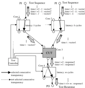
We present a new test methodology for SoCs based on consecutive testability. Figure 2 illustrates a consecutively testable SoC and the consecutive test access. A control sig- nal is provided for each core by a test controller (either off-chip or on-chip). Each control signal of a core deter- mines the current test mode of the core called a configu- ration. In Figure 2, a configuration of each core is deter- mined and consecutive transparencies of shaded ports are
CUT
Test Sequence
time t : vector1 time t : vector1’
Test Sequence
time t +2 : response2 time t +1 : response1
time t +1+ m : response1 PO
PI PI
Test Controller
selected consecutive transparency not selected consecutive transparency
latency: l cycles latency: k cycles
latency: m cycles time t +2 - k : vector3 time t +1 - k : vector2 time t - k : vector1 time t +2 - l : vector3’
time t +1 - l : vector2’ time t - l : vector1’
Test Response Core 1
Core 2
Core 3
Core 4
Figure 2. Consecutive Test Access realized. Consecutive transparency of an input port guaran- tees that any input sequence applied to the input port can propagate to some output ports consecutively at speed of system clock , and consecutive transparency of an output port guarantees that any output sequence that appears at the output port can propagate from some input ports consecu- tively at speed of system clock. Consecutive testability of an SoC guarantees that, for each core (interconnect) in the SoC, by selecting configurations of other cores, test patterns can be consecutively fed into the core (interconnect) from PIs and the responses can be consecutively propagated to POs through consecutive transparencies of other cores and interconnects. We define the consecutive transparency of a core and the consecutive testability of an SoC in the follow- ing subsections.
3.1 Consecutive Transparency
In this subsection, we define a new testability of a core called consecutive transparency as follows.
Definition 1: Let I i be the ith bit of an input port I, and O j be the jth bit of an output port O. Suppose that there exists a configuration of a core which can realize a path P between I i and O j . P is called a consecutively transparent pathif any input sequence applied to I i can be consecutively observed at O j after some latency, and then I i and O j are said to be consecutively transparent. Moreover, a core is called to be consecutively transparent if, for each port of the core, there exists a configuration that can make all bits of the port consecutively transparent.
Figure 3 illustrates various configurations of a consec- utively transparent core. A consecutively transparent core has generally several configurations, and each configuration can be identified by an ID number. By selecting a configu- ration of a core, consecutively transparent paths of an I/O
w1 w2 w3 w4 w5
w6 I1
w7 w8
(a) Configuration ID 1 (b) Configuration ID 2 (c) Configuration ID 3
(d) Configuration ID 4 (e) Configuration ID 5 PA
JA
PO PA
PA PO
JA JA
W(Ii) : bitwidth of an input port Ii W(Oi) : bitwidth of an output port Oi wi : bitwidth of consecutive transparent path
I2 I3
O1 O2
I1
I2 I3
O1 O2
I1
I2 I3
O1 O2
I1
I2 I3
O1 O2
I1
I2 I3
O1 O2
W(I1) = w1 W(I2) = w2 + w3 W(I3) = w4 = w5
W(O2) = w7 + w8 W(O1) = w6
Figure 3. Various Configurations of a Consec- utively Transparent Core
port are realized and the I/O port can be made consecutively transparent. For each configuration, all consecutively trans- parent paths between an input port and an output port are represented as one consecutively transparent path.
We classify consecutively transparent paths into three types, PA (Propagation AND), PO (Propagation OR), and JA(Justification AND). PA and PO are types of consecu- tively transparent paths for input ports to propagate test re- sponses. JA is a type of consecutively transparent paths for output ports to justify test sequences. Figure 3(a) illustrates type PA such that any input sequence applied to an input port I1propagates to only one output port O2. Figure 3(b) illustrates type PA such that any input sequence applied to an input port I2propagates to two output ports(O1and O2), where any input sequence of bit width W I2 is bit-sliced (W I2 w2 w3) and observed at two output ports (O1
and O2). Figure 3(c) illustrates type PO such that any in- put sequence applied to I3 propagates to two output ports (O1and O2), where any input sequence of bit width W I3
is fanouted (W I3 w4 w5) and observed at two output ports (O1and O2).
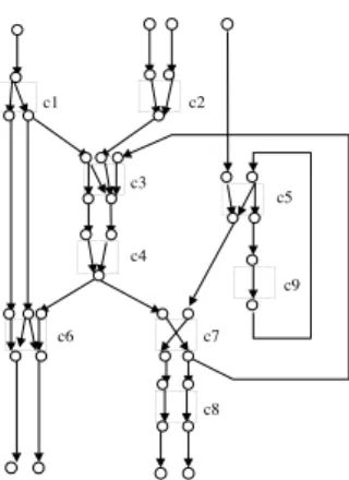
We define a core connectivity graph G V E λ to rep- resent an SoC composed of consecutively transparent cores:
V VPI VPO Vin Voutwhere VPIis the set of all PIs of the SoC, VPOis the set of all POs of the SoC,
Vinis the set of all input ports of cores in the SoC, and Voutis the set of all output ports of cores in the SoC. E Ecore Enet where
Ecore x y Vin Vout input port x is connected to output port y by a consecutively transparent path , and
Enet y x Vout Vin output port y is connected to input port x by an interconnect .
Labeling functionλ : E 2C I T Wwhere Cis the set of all cores in the SoC,
Iis the set of all ID numbers of configurations, T JA JO PA PO types of consecutively transpar- ent path (JO is for fanouted interconnects) , and Wis the set of all bit widths of e E.
Especially for e Enet,
λ e φ φ JO bit width of e φ φ PO bit width of e
c1 c2
c3
c4
c5
c6
c8 c7
c9
Figure 4. Core Connectivity Graph
e1 e2
e3
e4 e5
e1 : {{c, 2, PA, w2}, {c, 4, JA, w6}} e2 : {{c, 2, PA, w3}}
e3 : {{c, 1, PA, w1}, {c, 5, JA, w7}} e4 : {{c, 3, PO, w4}}
e5 : {{c, 3, PO, w5}, {c, 5, JA, w8}}
Figure 5. Label byλ
Figure 4 illustrates a core connectivity graph G which corresponds to the SoC of Figure 1 and Figure 5 illustrates edges labeled byλ which correspond to the core of Figure 3.
We refer to a vertex that has no input edge as a source, and a vertex that has no output edge as a sink. For a core connectivity graph G, selecting a configuration of a core is to leave edges which have labels of the configuration and to remove other edges from the core.
3.2 Consecutive Testability
In this subsection, we introduce a new testability of an SoC called consecutive testability. For SoCs, it is important to test timing faults such as delay faults as well as logic faults such as stuck-at faults. For that reason, it is necessary to be able to apply any test sequence from PIs to each core and observe any response sequence at POs consecutively at speed of system clock. Moreover, it is also important to test interconnects between cores thoroughly. We formalize consecutive testability of an SoC as a sufficient condition that satisfies above-mentioned conditions. We first define justification subgraph GJand propagation subgraph GP as follows.
Definition 2: Let G V E λ be a core connectivity graph of an SoC and GJ VJ EJ λ be an acyclic subgraph of G. For a core c C, GJis called a justification subgraph of c and c is said to be consecutively controllable if GJsatisfies all the following conditions.
1. All input ports of c are sinks in GJ and only PIs are sourcesin GJ.
2. For each edge u EJ, u has a label of either JO or JA.
3. Let G V E λ be a subgraph of G obtained by selecting a configuration for each core. For each edge u EJ,
(a) u contains all input edges of u in G , and (b) u contains only one output edge of u in G when
output edges have labels of JO in G .
Definition 3: Let G V E λ be a core connectivity graph of an SoC and GJ VJ EJ λ be an acyclic subgraph of G. For an interconnect e y x Enet, GJis called a justifi- cation subgraph of eand e is said to be consecutively con- trollableif GJsatisfies all the following conditions.
1. Only y is a sink in GJand only PIs are sources in GJ. 2. For each edge u EJ, u has a label of either JO or JA. 3. Let G V E λ be a subgraph of G obtained by selecting a configuration for each core. For each edge u EJ,
(a) u contains all input edges of u in G , and (b) u contains only one output edge of u in G when
output edges have labels of JO in G .
Definition 4: Let G V E λ be a core connectivity graph of an SoC and GP VP EP λ be an acyclic subgraph of G. For a vertex v V, GPis called propagation subgraph of vand v is said to be consecutively observable if GPsatisfies all the following conditions.
1. Only POs are sinks in GPand only v is a source in GP. 2. For each edge u EP, u has a label of either PO or PA. 3. Let G V E λ be a subgraph of G obtained by selecting a configuration for each core. For each edge u EP,
(a) u contains all output edges of u in G when the output edges have labels of PA, and
(b) u contains only one output edge of u in G when the output edges have labels of PO in G . Then, we define the consecutive testability of an SoC as follows.
Definition 5: Let G V E λ be a core connectivity graph of an SoC. An SoC is said to be consecutively testable if the SoC satisfies the following two conditions.
1. For each output port v Voutof each core c C, there exist one justification subgraph GJof c and one propa- gation subgraph GPof v where GJand GPare disjoint. 2. For each interconnect e y x Enet, there exist one justification subgraph GJ of y and one propagation subgraph GPof x where GJand GPare disjoint. 4 DFT for Consecutive Testability
This section presents a method for design-for-testability (DFT) that makes a given SoC consecutively testable. We assume that each individual core is testable and a precom- puted test set is available for each core which, if applied to the core, will result in a very high fault coverage, and the internal design of the cores cannot be modified by DFT due to IP (Intellectual Property) protection. Additionally, we as- sume that all cores are consecutively transparent and control signals for configurations can be controlled independently of normal operations. Even if a core is not consecutively transparent, we can make the core consecutively transpar- ent by adding bypass routes outside the core. In the rest of
this paper, we consider the DFT under such assumptions. 4.1 Problem Formulation
Each core (each interconnect) in a consecutively testable SoC is consecutively controllable and consecutively ob- servable. In other words, for each output port of each core (for each interconnect), a core connectivity graph G that represents a consecutively testable SoC has one justification subgraph GJ and one propagation subgraph GPwhere GJand GPare disjoint. When a given SoC does not have such disjoint subgraphs, paths from PIs and paths to POs are added using test MUXs (multiplexers) in the proposed DFT.
Definition 6: The DFT for the consecutive testability is for- malized as the following optimization problem.
Input: An SoC ( a core connectivity graph) Output: A consecutively testable SoC
Optimization: Minimizing hardware overhead (i.e., total bit width of added MUXs)
4.2 DFT algorithm
We propose a DFT algorithm for consecutive testability. The algorithm consists of the following four stages. Stage 1: Augment a given SoC so that all cores are consecutively controllable.
Stage 2: Augment a given SoC so that all cores are consecutively observable.
Stage 3: Augment a given SoC so that all interconnects are consecutively controllable.
Stage 4: Augment a given SoC so that all interconnects are consecutively observable.
Due to limitations of space, we only present a procedure of stage 1. However procedures for the other stages can be presented in a similar fashion.
4.2.1 DFT for Consecutive Controllability of Cores (Stage 1)
The objective of the first stage is to modify a given SoC with minimum hardware overhead so that all cores are consecutively controllable (i.e., all cores have justification subgraphs). The strategy of the algorithm is that, for each core, first it creates control initial graph, and second it creates control middle graph. Then it induces conditions such that each core has a justification subgraph (each core is consecutively controllable), and formalizes the DFT as integer programming problem. Justification subgraphs of all cores are determined with minimum hardware overhead by solving the integer programming problem.
Step 1: Creation of Control Initial Graph
The control initial graph GJcof a core c Cis created from a core connectivity graph G as follows.
1. Remove the edges which have labels of c and let the vertices which correspond to the input ports of c be sinks.
c1 c2
c3
c4
c5
c6
c8 c7
c9
1 1 1
1
1
1 1
2
2 2
AJc6 = {c1,c2,c3,c4,c7} BJc1 = {1} BJc2 = {1} BJc3 = {1,2} BJc4 = {1,2} BJc7 = {1}
KJc6 = {{1,1,1,1,1},{1,1,1,2,1} {1,1,2,1,1},{1,1,2,2,1}}
Figure 6. Control Initial Graph GJc6
2. Remove the edges which have labels of neither JA nor JO.
3. We define the control initial graph GJc as the set of vertices and edges reachable to sinks.
Figure 6 illustrates a control initial graph GJc6. Each edge in GJc6 has a label of either JO or JA and the num- ber beside e Ecorerepresents a label of configuration ID.
Let AJcbe the set of cores that exist in GJc. Here, a core c Cthat exists in GJc means that there exists more than one edge which has a label of c in GJc. For each a AJc, let BJa be the set of all configuration IDs of a. We define KJc
as the following equation.
KJc
∏
a AJc
BJa
BJa1 BJa2 BJa3
A control initial graph GJc contains several configurations for each core a AJc, and consecutive transparency of each core a AJcis not realized.
Step 2: Creation of Control Middle Graph
For each k KJc, the control middle graph GJc k is cre- ated from a control initial graph GJcas follows.
1. For each a AJc, select a configuration that corre- sponds to k.
2. We define the control middle graph GJc kas the set of vertices and edges reachable to sinks.
Figure 7 illustrates a control middle graph GJc6 k1. JO and JA beside e Erepresent types of consecutively trans- parent path e. A control middle graph GJc k contains only one configuration for each core a AJc, and consecutive transparency of each core a AJcis realized.
For GJc k, we define QJc k as the set that, for each q QJc k, q satisfies the following conditions.
1. q is a source and not an element of VPI.
2. q has more than two output edges which have labels of JO.
3. There exist cycles which contain q.
GJc k is not a justification subgraph GJbecause of vertices in QJc k. Thus, GJc kis a justification subgraph if the set QJc k
is empty, and we can make c consecutively controllable by
c1
c2
c3
c4
c6 c7
k1= {1,1,1,1,1} QJc6 = {v2} JA
JO JA
JA
JA JO JO
JO JO v2
Figure 7. Control Middle Graph GJc6 k1
c1
c3
c6 c4 v2 ei
c1
c3
c6 c4 v2 ei
Figure 8. Insertion of a MUX for Consecutive Controllability
selecting configurations of a AJcwhich correspond to k. Step 3: Integer Programming Formulation
Let Ycbe a variable that represents consecutive control- lability for c C, and let xei be a variable defined as fol- lows.
xei 1 if a test MUX is inserted to ei Enet
0 otherwise (1)
Figure 8 illustrates that a test MUX is inserted to ei. We can formalize the DFT for consecutive controllability of cores as the following integer programming problem: Minimize:
∑
ei Enet
xei bitwidth ei (2)
Subject to:
Yc 1 f or all c C (3)
xei 0 1 ei Enet (4)
Let Yc kbe a variable that represents consecutive control- lability for a control middle graph GJc k, and let Yc kq be a variable that represents consecutive controllability for a ver- tex q QJc k. Ycis defined as follows.
Yc
∑
k KJc
Yc k (5)
Yc k
∏
q QJc k
Yc kq (QJc k φ)
1 (QJc k φ)
(6)
Equation(5) means that core c is consecutively control- lable if c is consecutively controllable for more than one control initial graph GJc kby selecting configurations which correspond to k KJc. Equation(6) means that GJc kis a jus- tification subgraph if QJc k is empty or GJc k can be made consecutively controllable for all vertices in QJc k.
Yc kq is defined with xeias follows.
Case 1: q is a source of GJc kand not an element of VPI. Let S be the set of all simple paths from q to sinks in GJc k. In order to make GJc k consecutively controllable for q, it is sufficient that more than one MUX is inserted to each s Sand paths from PIs are added. Let Esbe the set of all edges which are elements of Enet in s. Insertion of more than one MUX to a simple path s means that msrepresented by the following equation is more than 1.
ms
∑
ei Es
xei (7)
With this ms, Yc kq is defined as follows. Yc kq
∏
s S
ms (8)
Case 2: q has more than two output edges which have labels of JO.
Let R be the set of all output edges of q in GJc k. For each r R, let Srbe the set of all simple paths that contain r from qto sinks. In order to make GJc kconsecutively controllable for q, it is sufficient that the following condition is satis- fied for more than one element r R. The condition is that ,for each r R r , more than one MUX is inserted to each s Sr and paths from PIs are added. Therefore, Yc kq is defined as follows with msrepresented by equation(7).
Yc kq
∑
r R r
∏
R r∏
s Sr
ms (9)
Case 3: There exist cycles which contain q.
Let S be the set of all cycles that contain q in GJc k. In order to make GJc k consecutively controllable for q, it is sufficient that more than one MUX is inserted to each s S and paths from PIs are added. Therefore, Yc kq is defined as follows with msrepresented by equation(7).
Yc kq
∏
s S
ms (10)
Test MUXs are inserted to the edges obtained by solving the integer programming problem with equations (2), (3), and (4). Thus, justification subgraphs of all cores can be determined with minimum hardware overhead.
5 Conclusions
In this paper, we introduced a new concepts of testability called consecutive transparency and consecutive testability. For a consecutively testable SoC, testing can be performed as follows. Test patterns of a core are propagated to the core inputs from the SoC inputs consecutively at speed of system clock. Similarly the test responses are propagated to the SoC outputs from the core outputs consecutively at speed of system clock. The propagation of test patterns
and responses is achieved by using the consecutive trans- parency properties of surrounding cores and interconnects between cores. All interconnects can be tested in a similar fashion. Therefore, the method can test not only logic faults such as stuck-at faults, but also timing faults such as delay faults that require consecutive application of test patterns at speed of system clock. We also proposed a design-for- testability (DFT) method for making a given SoC consecu- tively testable based on integer programming problem.
One of our future works is to propose a DFT method for making cores consecutively transparent. In this paper, we assumed that TPS and TRS are implemented off-chip, that is, external testing only. However, we also have to consider Built-In-Self-Testing (BIST). Hence, another future work is to extend the proposed SoC model to the SoC model with on-chip TPS and TRS and BISTed cores.
Acknowledgments
This work was sponsored in part by NEDO (New En- ergy and Industrial Technology Development Organization) through the contract with STARC (Semiconductor Technol- ogy Academic Research Center) and supported in part by Foundation of Nara Institute of Science and Technology under the Grant for Activity of Education and Research. Authors would like to thank Toshimitsu Masuzawa (Osaka University), Michiko Inoue and Satoshi Ohtake (Nara Insti- tute of Science and Technology) for their valuable discus- sion.
References
[1] Y.Zorian, E.J.Marinissen and S.Dey, ”Testing embedded-core based system chips,” Proc. Interna- tional Test Conference, pp.130-143, Oct. 1998. [2] S.Bhatia, T.Gheewala and P.Varma, ”A unifying
methodology for intellectual property and custom logic testing,” Proc. International Test Conference, pp.639-648, Oct. 1996.
[3] T.Ono, K.Wakui, H.Hikima, Y.Nakamura and M.Yoshida, ”Integrated and automated design-for- testability implementation for cell-based ICs,” Proc. Asian Test Symposium, pp.122-125, Nov. 1997. [4] N.A.Touba and B.Pouya, ”Testing embedded cores us-
ing partial isolation rings,” Proc. VLSI Test Sympo- sium, pp.10-16, May 1997.
[5] L.Whetsel, ”An IEEE 1149.1 based test access archi- tecture for ICs with embedded cores, ” Proc. Interna- tional Test Conference, pp.69-78, Nov. 1997. [6] I.Ghosh, N.K.Jha and S.Dey, ”A low overhead de-
sign for testability and test generation technique for core-based systems-on-a-chip,” IEEE Trans. on CAD, vol.18, no.11, pp.1661, Nov. 1999.
[7] I. Ghosh, S. Dey, and N.K. Jha, ” A fast and low cost testing technique for core-based system-on-chip,” Proc. 35th Design Automation Conference, pp.542- 547, June 1998.
[8] M.Nourani and C.A.Papachristou, ”Structural fault testing of embedded cores using pipelining,” Jour- nal of Electronic Testing:Theory and Applications 15, pp.129-144 1999.