An Efficient Scan Tree Design for Test Time Reduction
*Y. Bonhomme
1T. Yoneda
1H. Fujiwara
1P. Girard
21 Graduate School of Information Science, Nara Institute of Science and Technology Email: {bonhomme, yoneda, fujiwara}@is.naist.jp
2LIRMM, UMR 5506 Université Montpellier II/CNRS, France Email: [email protected]
Abstract: We propose a new scan tree architecture for test application time reduction. This technique is based on a dynamic reconfiguration mode allowing one to reduce the dependence between the test set and the final scan tree architecture. The proposed method includes two different configuration modes: the scan tree mode and the single scan mode. The proposed method does not require any additional input or output. Experimental results show up to 95% of test application time saving and test data volume reduction in comparison with a single scan chain architecture.
Keywords: DfT, Scan Testing, Scan Tree
1. Introduction
The controllability and the observability of complex designs are nowadays guaranteed by DfT techniques. The full scan design is the most popular DfT technique [1] and it is very largely used in integrated circuits (ICs) or in System on chip (SoC) cores. Unfortunately, scan based architectures are expensive in test power consumption [2] and in test application time.
The test application time depends on the scan chain length. Indeed, the number of clock cycles required to scan in/out the test data is equal to the product of the number of test patterns by the scan chain length. The test sequence cannot be reduced without degrading the test quality. Thus, one solution to save test application time is to lessen the scan chain length.
At present, multiple scan chain design is often used to reduce the scan test shift time. This technique consists of splitting the scan chain in small scan sub-chains activated at the same time. The size of the different scan segments can be fixed [3,4] or variable [5,6]. Multiple scan chain design is now a standard [1] often used in ICs and in SoC cores (using the IEEE P1500 standard). The main drawback of this technique is the increase of the number of scan inputs and outputs dedicated to the test. Different techniques allow one to reduce the
test application time with a low increase of the number of scan inputs and outputs [7-18].
Some solutions are based on test encoding [7- 13]. The use of these techniques requires extra DfT logic. The hardware overhead of the decompressor is directly linked to the compression ratio.
Other solutions propose to reduce the test time without encoding process [14,15] and with a single scan input to drive several scan chains. The main drawback is a reduction of the circuit controllability. A dynamic reconfiguration can be used to improve the circuit controllability [15], but an additional test control input is then required.
Scan tree design is often used to deal with different scan DfT technique problems like test power [19] or test time [17,18]. The idea of scan tree design is that one scan cell drives other scan cells. This technique is interesting for test time reduction and it is a serial/parallel scan design with a single scan input. The same test data must be stored in different scan cells. The circuit controllability is reduced and this method requires a full compatibility between the parallel scan cells. So the effectiveness of a scan tree architecture depends on the correlation between the test data of the different scan cells. The first technique [17] proposes to reduce this dependence by increasing the number of don’t care values of the test sequence. But the solution effectiveness still depends on the circuit structure. The second technique [18] adopts a folding mode allowing one to increase the parallelism of the scan tree architecture. However, test sequence updating during the manufacturing phase but also the circuit time life, is impossible with both techniques.
In this paper, we propose an optimal scan tree architecture for test shift time reduction. The idea is to use a dynamic reconfiguration during the test application to switch from a scan tree mode to a single scan mode. A part of the test sequence is applied in scan tree mode to save test application time and the other part is applied in single scan mode. This procedure allows one to reduce the dependence between the scan tree architecture and the test sequence. With the proposed technique, it is possible to update the test sequence. This procedure
* This work has been supported in part by 21st Century COE Program"Ubiquitous Networked Media Computing".
9th IEEE European Test Symposium (ETS'04) , pp. 174-179, May 2004.
does not require additional test control input. A MISR is used for the circuit response compaction.
This paper is organized as follows. In section 2, a preliminary about full compatible scan tree architecture is presented and the proposed technique is described. In section 3, the scan tree generation of the proposed method is explained. Section 4 shows some experimental results for benchmark circuits and section 5 concludes the paper.
2. Proposed scan tree architecture
2.1 Preliminary (full compatible scan
tree architecture)
Recently, two scan tree architectures [17,18] have been proposed to reduce the test application time. The basic principle of these techniques is described in figure 1. The idea is to store at the same time the similar test data in different scan cells. A computation of the test sequence is required to form groups of compatible scan cells that can receive the same test data.
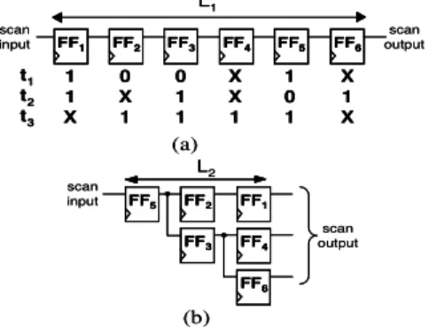
Figure 1. Example of scan tree architecture generation
Figure 1.a presents an example of a single scan chain composed of 6 scan cells (FF1 to FF6) and the associated test set. From this data, groups of compatible scan cells are created {FF1, FF4 and FF6}, {FF2 and FF3} and {FF5}. Scan cells of the same group must receive the same test data. FF2
and FF3 can be placed in the same group as far as they receive the same test data, respectively 0X1 and 011. FF5 is incompatible with all other scan cells. From these groups, scan tree architecture is generated and represented in figure 1.b. The test shift time saving corresponds to the ratio of the difference between L1 and L2 over L1, where L1
corresponds to the single scan chain length and L2
to the scan tree length. Moreover, a reduction of the test data volume is obtained. This reduction is equivalent to the test shift time saving.
To generate scan tree architectures, full compatibility between the FFs of the same group is required. This full compatibility creates a high dependence between the scan tree architecture and the test sequence. To reduce this dependence, we propose a new scan tree architecture.
2.2 Proposed architecture
In this part, we present the proposed scan tree method. This method generates an optimal scan tree design with a dynamic reconfiguration during test application. The dynamic reconfiguration consists in switching between two modes. The first mode is the scan tree mode (ST mode) and the second one is the single scan mode (SS mode). The idea is to apply a part of the test sequence in ST mode and the other part in SS mode. This technique allows one to reduce the dependence between the scan tree architecture and the test sequence and to improve the test shift time reduction.
Figure 2. Proposed scan tree architecture Figure 2 describes the proposed scan tree architecture. The switch functionality from ST mode to SS mode is carried out by a pattern recognition module, multiplexers and a flip-flop driven by the scan enable signal (in grey color in figure 2). The activation occurs when the last test pattern of the scan tree mode has been applied. This extra DfT logic has a low impact on the area overhead. A MISR is used for the response compression. Figure 3 presents the two configurations of the architecture: in 3.a the ST mode and in 3.b the SS mode. In both cases, there is only one scan input and one scan output and a single test control input.
Figure 3. Two modes: a/ scan tree mode b/ single scan mode
1 1 X
0 X 1
0 1 1
X X 1
1 0 1
X 1 X t1
t2 t3
FF6 FF5 FF4 FF3 FF2 FF1
FF1
FF4
FF6 FF2
FF3 FF5 scan
input
scan input
scan output
scan output
(a)
(b) L1
L2 1
1 X
0 X 1
0 1 1
X X 1
1 0 1
X 1 X t1
t2 t3
FF6 FF6 FF5 FF5 FF4 FF4 FF3 FF3 FF2 FF2 FF1 FF1
FF1 FF1
FF4 FF4
FF6 FF6 FF2 FF2
FF3 FF3 FF5 FF5 scan
input
scan input
scan output
scan output
(a)
(b) L1
L2
M I S R
Scan input
Scan output Pattern Recognition
Scan enable
M I S R
Scan input
Scan output Pattern Recognition
Scan enable
M I S R Scan
input
Scan output
M I S R Scan
input
Scan output (a)
(b) Pattern Recognition
Scan enable
Pattern Recognition
Scan enable
M I S R Scan
input
Scan output
M I S R Scan
input
Scan output (a)
(b) Pattern Recognition
Scan enable
Pattern Recognition
Scan enable
Concerning design constraints (fanout limitation for the scan cells and routing), we shall try to consider them in further work. Clustering process already proposed in [20] may be used. The configuration flexibility of the proposed scan tree architecture should allow one to obtain a good trade-off between test time reduction and design constraints.
To design the scan tree architecture, it is necessary to find the optimal balance between the part of the test sequence to apply in ST mode and the other part to apply in SS mode. The next section presents the adequate scan tree architecture generation procedure.
3. Scan tree architecture generation
Scan tree architecture generation consists in finding the good balance between the part of the test sequence to apply in ST mode and the other part to apply in SS mode. The complexity of scan tree architecture generation to find the optimal solution depends on the number of test patterns and scan cells. This problem is NP-complete. The following section describes different heuristics to reduce the problem complexity. Section 3.1 presents the adopted solution of scan tree generation and section 3.2 details the solution to determine the part of the test sequence to apply in ST mode.
3.1 Scan tree generation
Scan tree generation consists of finding groups of compatible scan cells from a test set. We construct the incompatibility graph from the test set and adopt a vertex coloring process for the graph to solve the problem of finding optimal groups of compatible scan cells. In an incompatibility graph for a test, a vertex corresponds to a scan cell, and edge between two vertices exists if two scan cells corresponding to the vertices are incompatible in the test set.
Figure 4. a/ scan tree generation from a test pattern and b/ scan tree generation from 2 test
patterns
Figure 4 presents two examples of scan tree generation. In both, the scan chain is composed of 6 scan cells. In figure 4.a, scan tree architecture is generated via a coloring graph from the test pattern t1. The FF1 is incompatible with the FF2, FF3 and FF6. These incompatibilities are reported by edges between (FF1, FF2), (FF1, FF3) and (FF1, FF6). The complexity of the coloring graph algorithm is O(n2), n corresponding to the number of scan cells. Figure 4.b corresponds to the addition of the test pattern t2
to the previous solution for t1. The addition of the pattern t2 increases the number of incompatibilities and coloring graph edges. In consequence, the length of the scan tree grows to 3 cells instead of 2. With this example, we show that the scan tree architecture has a high dependence with the test patterns. Test pattern selection must be achieved to determine the part of the test sequence to apply in ST mode.
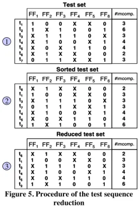
Figure 5. Procedure of the test sequence reduction
3.2 Test pattern selection
The test pattern selection problem is reduced to Traveling Salesperson Problem (TSP [21]). It is not possible to find an exhaustive solution to determine the part of the test sequence that should be applied in ST mode. The complexity of the problem resolution depends on the number of test patterns. To reduce the complexity, a test sequence reduction procedure is applied. This procedure is described in figure 5. The first step is to compute the number of incompatibilities for each test pattern. The number of incompatibilities corresponds to the number of edges in the coloring graph. The second step consists in sorting the test sequence according to the number of incompatibilities. The last step
FF1 FF2 FF3 FF4 FF5 FF6 1
1 X X X X 0
0 X 1 1 0 1 1
0 1 1 0 X X 1
X 0 1 0 1 X X
X 0 0 X 1 0 X
0 1 X 1 0 0 1 t1
t2 t3 t4 t5 t6 t7
3 6 3 4 4 2 3
#imcomp.
FF1 FF2 FF3 FF4 FF5 FF6 X
1 X 0 X X 1
1 0 1 1 1 0 X
X 0 1 1 0 X 1
X X 1 X 0 1 0
0 X 0 X X 1 0
0 0 X 1 1 0 1 t6
t1 t3 t7 t4 t5 t2
2 3 3 3 4 4 6
#imcomp.
FF1 FF2 FF3 FF4 FF5 FF6 X
1 X X X 1
1 0 1 1 0 X
X 0 1 0 X 1
X X 1 0 1 0
0 X 0 X 1 0
0 0 X 1 0 1 t6
t1 t3 t4 t5 t2
2 3 3 4 4 6
#imcomp.
Test set
Sorted test set
Reduced test set
1
2
3
t1: 100XX0 FF1 FF2
FF3 FF4
FF5
FF6 FF1
FF4
FF5 FF2
FF6 FF3
scan input
scan output M
I S R L1=2
(a)
Coloring graph Scan tree architecture
FF1
FF2
FF3 FF4
FF5
FF6 FF1 FF4
FF5 FF2
FF6 FF3
scan input
scan output M
I S R L1=3
Coloring graph (b) t1: 100XX0
t2: 1X1001
t1: 100XX0 FF1 FF2
FF3 FF4
FF5
FF6 FFFF11
FF4 FF4
FF5 FF5 FF2 FF2
FF6 FF6 FF3 FF3
scan input
scan output M
I S R L1=2
(a)
Coloring graph Scan tree architecture
FF1
FF2
FF3 FF4
FF5
FF6 FFFF11 FFFF44
FF5 FF5
FF2 FF2
FF6 FF6 FF3 FF3
scan input
scan output M
I S R L1=3
Coloring graph (b) t1: 100XX0
t2: 1X1001
Table 1. Experimental results on ISCAS`89 benchmark circuits
Table 2. Experimental results on ITC’99 benchmark circuits Benchmark
reference
# FFs
# test patterns
FC (%)
# clock cycles for
single scan
(1)
# clock cycles for scan tree (2)
# clock cycles for
the proposed method (3)
test time saving
(%) (1)(2)
test time saving
(%) (1)(3)
computation time (sec)
b09 28 51 99.72 1,428 1,071 848 25 40.62 0.01
b10 17 102 100 1,734 918 712 47.06 58.94 0.01
b11 31 111 97.11 3,441 1,887 633 45.16 81.6 1
b12 121 183 99.96 22,143 6,954 4,441 68.6 79.94 15
b13 53 52 96.43 2,756 1,508 876 45.28 68.21 1
b14 245 906 97.07 22,1970 110,532 22,450 50.2 89.89 869
reduces the test sequence by removing the equivalent test patterns defined as follows.
Definition: a test pattern is equivalent to another test pattern if they have the same incompatibility graph. In the example of figure 5, the two patterns t1 and t7 can be applied with the same scan tree design.
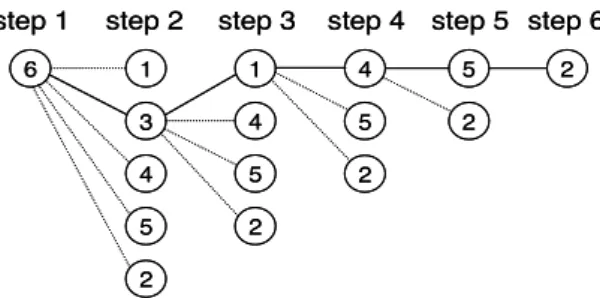
Figure 6. Test pattern selection procedure To determine the part of the test sequence to apply is ST mode, we use a greedy algorithm whose complexity is equal to O(m2) (m corresponding to the test sequence length). Figure 6 represents the test pattern selection procedure. The nodes represent test patterns. The first node is the pattern with the smallest number of incompatibilities. From this first test pattern, a scan tree architecture is obtained (step 1). We then try to include another test pattern (step 2). For all the possible nodes of the step 2 (node 1 to node 5) we build the corresponding scan tree architecture including the first node and the current node. We choose to include in the solution the test pattern that
implies the lowest increase of the scan tree length. This operation is repeated until all nodes are included (steps 3 to 6). The final step (step 6) corresponds to the full compatibility scan tree including all the test sequence. At each step, the number of clock cycles required to apply the test sequence is computed. The final solution is given by the step with the lowest number of clock cycles.
Finally, the complexity of the complete scan tree architecture generation is O(m2*n2). In further work, we will try to find a solution to reduce the complexity in order to save computation time.
4. Experimental results
We have implemented the proposed method in C language on a Pentium M 1.6 GHz with 512 MB and have applied it to ISCAS’89 and ITC’99 benchmark circuits. The test sets used are provided by Testgen tool [22] from Synopsys.
Table 1 and 2 give the results respectively for ISCAS’89 and ITC’99 benchmark circuits. The first four columns of the tables describe the circuits names, numbers of scan cells, lengths of test sequences (without any compaction) and corresponding fault coverages. The three following columns report the number of clock cycles (corresponding to the scan in/out operations only) for the single scan chain, the full compatible scan tree architecture and the proposed method respectively. The next two columns correspond to the test shift time savings (in percentage). The first one is the test shift time saving between the single scan chain and the full compatible scan tree Benchmark
reference
# FFs
# test patterns
FC (%)
# clock cycles for
single scan
(1)
# clock cycles for scan
tree (2)
# clock cycles for
the proposed method (3)
test time saving
(%) (1)(2)
test time saving
(%) (1)(3)
computation time (sec)
s1423 74 79 98.99 5,846 1,817 947 68.92 83.8 1
s5378 179 178 98.78 29,714 13,350 4,472 58.10 85.96 22
s9234 211 341 93.16 71,951 34,322 19,391 52.30 73.05 163
s13207 669 540 98.32 361,260 52,608 26,646 85.35 92.62 950
s15850 596 390 96.29 232,440 59,554 32,604 74.38 85.97 553
s38584 1426 1098 95.23 1,565,748 500,688 71,226 68.02 95.45 14,630
6
4 5 2 1
3 4
5 2
1 4
5 2
5 2
2 step 1 step 2 step 3 step 4 step 5 step 6
6
4 5 2 1
3 4
5 2
1 4
5 2
5 2
2 step 1 step 2 step 3 step 4 step 5 step 6
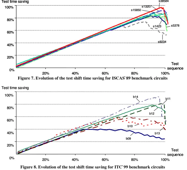
Figure 7. Evolution of the test shift time saving for ISCAS`89 benchmark circuits
Figure 8. Evolution of the test shift time saving for ITC`99 benchmark circuits architecture. The second one gives the test shift
time savings between the single scan chain and the proposed method. The last column reports the corresponding computation time in seconds.
The number of clock cycles is computed considering the following expression:
(
× 2)
+( ( )
× 1)
= #t L #t #t L cycles
_ clock
# st t st
where #tst is the number of test patterns applied in ST mode, L2 is the length of the scan tree architecture, #tt is the test sequence length and L1 is the number of scan cells. For single scan chain, #tst
is equal to 0. For full compatible scan tree, #tst is equivalent to #tt. For the proposed solution, #tst is included between 0 and #tt.
The test shift time saving using the full compatible scan tree is equal to 52.3% in average and to 78.9% at maximum in comparison with the single scan architecture. The proposed method improves significantly the test time reduction. Indeed, the average test shift time saving is equal to 78% and reaches 95.45% for s38584. The difference of time saving achievements clearly shows the effectiveness of the proposed solution. Moreover, an equivalent reduction of the test data volume is obtained. Concerning the computation
time, it remains reasonable even though the results have not been provided by a workstation.
Figures 7 and 8 represent the evolution of the test shift time saving along the amount in percentage of patterns in the test sequence applied in ST mode. A linear evolution of test shift time saving can be observed in the first part of the graphics. This linear evolution reveals that the test patterns progressively included in the solution have a low impact on the current scan tree architecture, implying a beneficial reduction of the test time. Full compatible scan tree architecture corresponds to the last point on the curve (100% of the test sequence is applied in scan tree mode)
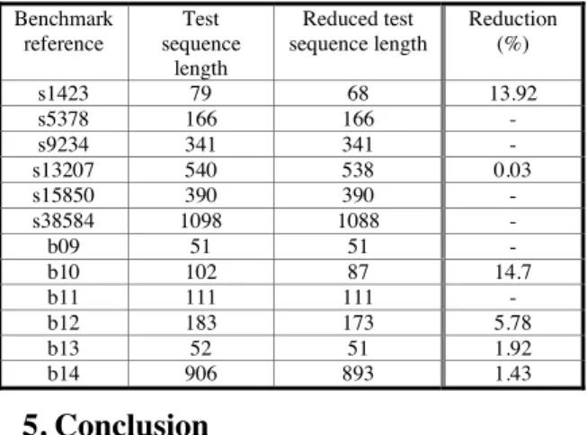
Concerning the effectiveness of the proposed test sequence reduction to lessen the scan tree architecture generation complexity, the table 3 summarizes the achieved results. The first column reports the names of the circuits. The second and third columns correspond respectively to the test sequence length and to the reduced test sequence length considered for the architecture generation algorithm. The last column reports the corresponding percentage of reduction. The results show the effectiveness of this solution for some 0%
20% 40% 60% 80% 100%
20% 40% 60% 80% 100%
b09 b10
b11
b12
b13 b14
Test time saving
Test sequence 0%
20% 40% 60% 80% 100%
20% 40% 60% 80% 100%
b09 b10
b11
b12
b13 b14
Test time saving
Test sequence
-
s5378
s9234 s15850
s13207
s38584
s1423
0% 20% 40% 60% 80% 100%
20% 40% 60% 80% 100%
Test time saving
Test sequence
s5378
s9234 s15850
s13207
s38584
s1423
0% 20% 40% 60% 80% 100%
20% 40% 60% 80% 100%
Test time saving
Test sequence 0%
20% 40% 60% 80% 100%
20% 40% 60% 80% 100%
Test time saving
Test sequence
circuits. In future work, we will try to improve the proposed solution to reduce thecomplexity of the scan tree architecture generation.
Table 3. Optimization of the test sequence for the scan tree architecture generation on ISCAS’89 and ITC99 benchmark circuits
5. Conclusion
In this paper, a new scan tree architecture is presented to reduce scan test shift time thanks to a dynamic reconfiguration during the test application. Experimental results for benchmark circuits show that our proposed method can reduce scan test shift time up to 95% of that for the single scan. In further work, we shall consider design constraints and reduce the scan tree generation complexity. Another perspective is to use several scan tree modes to improve the test time reduction.
Acknowledgments
We would like to thank Prof. Michiko Inoue, Prof. Satoshi Ohtake, and Dr. Mariane Comte of Nara Institute of Science and Technology for their valuable comments. This work was supported in part by 21st Century COE (Center of Excellence) Program "Ubiquitous Networked Media Computing" and in part by JSPS (Japan Society for the Promotion of Science) under Grants-in-Aid for Scientific Research B(2) (No. 15300018).
References
[1] M.L. Bushnell and V.D. Agrawal, “Essentials of Electronic Testing ”, Kluwer Academic Publishers, ISNB 0-7923-7991-8, 2000.
[2] P. Girard, “Survey of Low-Power Testing of VLSI Circuits”, IEEE Design & Test of Computers, Vol. 19, N° 3, pp. 82-92, May-June 2002.
[3] P.P. Fasang, J. P. Shen, M. A. Schuette and W. A. Gwaltney,
“Automated Design for Testability of Semicustom Integrated Circuits”, IEEE Int. Test conf. pp. 558-564, November 1985. [4] S. Kobayashi, M. Edahiro and M. Kubo, “Scan-Chain Optimization Algorithms for Multiple Scan-Paths”, IEEE Asia and South Pacific Design Automation Conf., pp. 301-306, February 1998.
[5] S. Narayanan, R. Gupta and M. A. Breuer, “Optimal Configuration of Multiple Scan Chains”, IEEE Trans. On Computers, Vol. 42, N° 9, pp. 1121-1131, September 1993.
[6] S. Bhawmik and P. Palchaudhuri, “DFT Expert: Designing testable VLSI Circuits”, IEEE Design Test, pp. 8-19, October 1989.
[7] J. Rajski, J. Tyszer, M. Kassab, N. Mukherjee, R. Thompsom, K. H. Tsai, A. Hertwig, N. Tamarapalli, G. Mrugalski, G. Eide and J. Qian, “Embedded Deterministic Test For Low Cost Manufacturing Test”, IEEE Int. Test Conf., pp. 301-310, October 2002.
[8] A. Chandra and K. Chakrabarty, “Frequency-Directed Run- Length (FDR) Codes with Application to System-on-a-chip Test Data Compression”, IEEE VLSI Test Symp., pp. 42-47, April 2001.
[9] A. Jas, J.G. Dastidar and N.A. Touba, “Scan Vector Compression /Decompression Using Statiscal Coding”, IEEE VLSI Test Symp., pp. 114-120, April 2000.
[10] A. Jas, B. Pouya and N.A. Touba, “Virtual Scan Chains’ A Means for Reducing Scan Length in Cores”, IEEE VLSI Test Symp., pp. 73-78, April 2000.
[11] S. Sybille, H.G. Liang and H.J. Wunderlich, “A mixed Mode BIST Scheme Based on Reseeding of Folding Counters”, IEEE Int. Test Conf., pp. 778-784, October 2000.
[12] W.B. Jone, J.C. Rau, S.C. Chang and Y.L. Wu, “A Tree- Structured LFSR Synthesis Scheme for Pseudo-Exhaustive Testing of VLSI Circuits”, IEEE Int. Test Conf., pp. 322-330, October 1998.
[13] I. Bayraktaroglu and A. Orailoglu, “Test Volume and Application Time Reduction through Scan Chain concealment”, Design Automation Conference, pp. 151-155, June 2001. [14] I. Hamzaoglu and J. H. Patel, “Reducing Test Application Time for Full Scan Embedded Cores”, Int. Symp. on Fault Tolerance Computing, pp. 260-267, July 1999.
[15] A.R. Pandey and J. H. Patel, “Reconfiguration Technique for Reducing Test Time and Test Data Volume in Illinois Scan Architecture Based Designs”, IEEE VLSI Test Symp., pp. 9-15, April 2002.
[16] K.L. Lee, J.J. Chen and C.H. Huang, “Using a Single Input to Support Multiple Scan Chains”, ICCAD, pp. 74-78, November 1998.
[17] k. Miyase and S. Kajihara, “Optimal Scan Tree Construction with Test Vector Modification for Test Compression”, IEEE Asian Test Symp., pp. 136-141, November 2003.
[18] H. Yotsuyanagi, T. Kuchii, S. Nishikawa, M. Hashizume and K. Kinoshita, “Reducing Scan Shifts using Folding Scan Trees”, IEEE Asian Test Symp., pp. 6-11, November 2003. [19] D. Xiang , S. Gu, J. G. Sun and Y. Wu, “A Cost-Effective Scan Architecture for Scan Testing with Non-Scan Test Power and Test Application Cost”, Design Automation Conf., pp. 744- 747, June 2003.
[20] Y. Bonhomme, P. Girard, L. Guiller, C. Landrault and S. Pravossoudovitch, “An Efficient Scan Chain Design for Power Minimization During Scan Testing Under Routing Constraint”, IEEE Int. Test Conf., pp. 488-493, October 2003.
[21] D.S. Johnson and L.A. McGeoch, “The Traveling Salesman Problem : A Case Study in Local Optimization”, in Local Search algorithms in Combinatorial Optimization, E.H.L. Aarts and J.K. Lenstra, eds. John Wiley and Sons, 1996.
[22] TestGen, Version 5.3, Synopsys Inc., 1999. Benchmark
reference
Test sequence
length
Reduced test sequence length
Reduction (%)
s1423 79 68 13.92
s5378 166 166 -
s9234 341 341 -
s13207 540 538 0.03
s15850 390 390 -
s38584 1098 1088 -
b09 51 51 -
b10 102 87 14.7
b11 111 111 -
b12 183 173 5.78
b13 52 51 1.92
b14 906 893 1.43