Defect Level vs. Yield and Fault Coverage in the
Presence of an Imperfect BIST
Yoshiyuki Nakamura*†, Jacob Savir‡ and Hideo Fujiwara*
*Nara Institute of Science and Technology (NAIST)
†NEC Electronics Corporation
‡New Jersey Institute of Technology (NJIT) Abstract Williams and Brown’s formula,
relating the product defect level as a function of the manufacturing yield and fault coverage, is re- examined in this paper. In particular, special attention is given to the influence of an imperfect built-in self-test (BIST) on this relationship. We show that when the BIST hardware is used to screen the functional product, an imperfect BIST circuitry tends to reduce the effective fault coverage and increase the corresponding product defect level.
1. Introduction
Williams and Brown [1] had shown the relationship between manufacturing yield and the fault coverage of the test process used to screen the product into either a good lot or a bad lot. This well-known relationship is derived assuming that the test equipment is perfect, i.e. fault-free.
Many chips today have BIST circuitry in them. These BIST circuits are used to test the chips and perform the screening described above. Since the BIST hardware is manufactured using the same technology and process as the functional circuits, it is unrealistic to assume that it is fault-free. It is, therfore, imperative to allow the BIST hardware be subjected (during the analysis) to the same defect level (impurity) as the functional circuits themselves. It is the subject of this paper to investigate the effect of an imperfect (i.e. possibly faulty) BIST environment on the William’s and Brown’s equation. In theory, the side effect of an imperfect BIST is to either cause a good product (i.e. no functional defects present) be declared faulty, resulting in a yield loss, or cause a bad product be passed
as good. In practice, however, the first side effect is the predominant one, while the second side effect has very low probability of actually occuring, and, therefore, can be ignored.
In [2,3] the effects of an imperfect tester on the resulting yield during a delay (AC) test is discussed. In [4,5] a more generalized fault probability model is introduced to enhance the defect vs. yield equation. In [6] an experiment using CrossCheck technology is conducted in order to evaluate the relationship between defect level and fault coverage.
This paper is organized as follows. Section 2 is a brief review of Williams and Brown’s formula. Section 3 derives the yield equation in BISTed products with imperfect BIST circuitry. We show that the Williams and Brown’s equation is a special case of our more generelized formula, i.e. our new formula reduces to Williams and Brown’s under perfect BIST circuitry. Section 4 discusses the properties of the newly derived formula by displaying the graphs of some typical case studies. Section 5 draws some conclusions from this analysis.
2. Recapitulation of Williams and
Brown’s Equation
Let the circuit under test (CUT) have n possible faults, each having the same probability of occurrence, p. The yield, Y, is the probability that the circuit is fault-free, i.e.
p n
Y =(1− ) (1) IEEE 5th Workshop on RTL and High Level Testing (WRTLT'04), pp. 79-84, Nov. 2004.
The raw defect level of the product coming out of the manufacturing line (without any test) is
p n
Y
D0 =1− =1−(1− ) (2) Assuming that the test process can detect m out of the n possible fault, the fault coverage is given by
n
F = m (3)
A circuit that passes the test is guaranteed to be free of any detectable fault (m in total), but can still possess an undetectable fault that escaped the test. Since there are n-m undetectable faults, the defect level after test is given by
m
p n
D=1−(1− ) − , (4) which can be further reduced to
n F m
n Y
p
D=1−[(1− ) ](1− ) =1− 1− (5) Thus, this equation assumes that the test process is fault-free, i.e. a circuit being declared by the test process to be faulty is truly faulty. This is the underlying assumption in the derivation of this formula.
3. Enhanced Equation in the
Presence of an Imperfect BIST
The product is assumed to have BIST circuitry besides its own functional circuits. The BIST hardware tests the functional circuits in order to determine whether they are faulty or fault- free. A product that fails the self-test is being discarded (or placed in the bad lot). A product may fail the test even when its functional piece is fault-free due to faulty BIST hardware. This is a clear case of a yield loss. In the sequel we will refer to the product functional circuits as the CUT. We use the following parameters in our analysis:
D – Product defect level after test under perfect BIST hardware
D’ - Product defect level after test under imperfect BIST hardware
F - Fault coverage of the CUT under perfect (fault-free) BIST hardware
F’ – Effective fault coverage of the CUT in the presence of an imperfect BIST
hardware Y - Product yield p - Fault probability
nc - Total number of possible faults in the CUT
nb - Total number of possible faults in the BIST hardware
m - Number of CUT faults covered by perfect (fault-free) BIST hardware
m’ - Expected number of CUT faults covered by an imperfect BIST hardware
k - Number of CUT faults covered by a faulty BIST hardware
mb - Number of BIST faults covered by the BIST hardware
α - Ratio between BIST area to the CUT area
ρ - Fault coverage reduction factor
µ - BIST circuitry fault coverage by its own test procedure
λ - Yield coefficient
The meaning of α , ρ, µ and λ will become evident from the following analysis.
Notice that we are allowing the test procedure conducted by the BIST hardware to cover k<m possible CUT faults when faulty. Also, the BIST hardware is assumed to cover mb< nb of its own faults.
We proceed to calculate m’, the expected number of CUT faults covered by BIST:
{
Good BIST}
k{
Bad BIST}
m
m'= ×Pr + ×Pr ] ) 1 ( 1 [ )
1
( p nb mb k p nb mb m − − + − − −
= (6)
The expected CUT fault coverage, as conducted by the BIST circuitry, is:
]} ) 1 ( 1 [
) 1 {( ]
) 1 ( 1 [
) 1 ' (
'
b b
b b b
b b b
m n
m n c
m n c
m n c
c
m p k
n p p m
n k
n p m n F m
−
−
−
−
−
− +
−
=
−
− +
−
=
=
Define:
m
= k
ρ (7)
to be the fault coverage reduction factor when the BIST circuitry is faulty. Then,
]} ) 1 ( 1 [
) 1 {( '
b b
b b
m n
m n
p p F F
−
−
−
−
+
−
=
ρ (8)
Eq. (8) can also be written as:
)] 1
( [
' c
b b c
b b
n m n n
m n
Y Y
F F
−
−
− +
= ρ (9)
The exponent in Eq. (9) can be written as
=
−
− = (1 )
b b c
b c
b b
n m n
n n
m n
λ µ
α(1− )= , (10)
where
c b
n
= n
α is roughly the ratio between the BIST circuitry area and the area of the CUT, and
b b
n
=m
µ is the BIST circuitry fault coverage as conducted by BIST itself. We call
) 1 ( µ α
λ= − the yield coefficient.
The effective fault coverage, F’, can now be written as
)] 1 ( [
' F Yλ ρ Yλ
F = + − (11)
The new formula relating the product defect level to the yield and the effective fault coverage becomes:
'
1 1
' Y F
D= − − (12)
Example 1: Consider a chip manufacturing line with 90% yield. The chips are screened using their BIST circuitry. The BIST circuitry constitutes 5% of the entire chip area. The BIST procedure has 95% coverage of the functional faults when assumed to be fault-free, and only 40% coverage when assumed faulty. The BIST procedure covers 30% of of its own faults. Compute the chip defect level after its BIST screening.
Solution: We have the following parameters:
19 1 955 =
α = , µ =0.3,
10 3
68 . 19 3
7 .
0 ≈ × −
λ= , 0.421
9540 ≈ ρ =
)] 9
. 0 1 ( 421 . 0 9
. 0 [ 95 . 0
'= 3.68×10⁻³ + × − 3.68×10⁻³
F
9498 .
≈0
3 0502
. 0 9498
. 0
1 1 0.9 5.275 10
9 . 0 1
'≈ − − ≈ − ≈ × −
D
ppm
≈5275
Notice that if we ignore the effects of the BIST, the defect level is:
3 05
. 0 95
. 0
1 1 0.9 5.254 10
9 . 0
1− − = − ≈ × −
= D
ppm
≈5254 ▄
It is interesting to take note of the following special cases:
(a) If there is no BIST circuitry (α =0), we have F'=F , and D'=D . This is the Williams and Brown’s case. Similarly, in the case where there is a BIST hardware with µ=1, the formulas also reduce to the Williams and Brown’s case.
(b) If the BIST procedure has zero coverage against functional faults while being itself faulty, then ρ=0 . The effective fault coverage then reduces to:
Yλ
F
F'= (13)
The impact of the BIST impurity on the product defect level can be best measured by the differential ∆D=D'−D. In most real–life cases F'≈F , λ ≈0 . By using calculus approximation techniques, and under the restrictions just described, ∆D can be approximated to be:
Y F
D≈ λ(1−ρ)ln2
∆ (14)
and the ratio D
∆D to be:
) 1 )( 1 (
ln ) 1
( 2
Y F
Y F
D D
−
−−
∆ ≈ λ ρ (15)
Example 2: Consider again the case described in Ex. 1. By using Eq. 14 we get:
9 . 0 ln ) 421 . 0 1 ( 10 68 . 3 95 .
0 × × 3× − × 2
=
∆D −
ppm
≈22
Compare this to the exact result of 21ppm
derived in Ex. 1. ▄
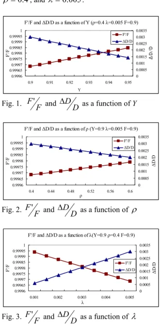
4. Some Typical Behavior
In order to see the trend of these newly derived formula, we plot
F'F and DD
∆ for
the parameter ranges 0.9≤ Y ≤0.95 , 99
. 0 9
.
0 ≤ F≤ , 0.4≤ρ ≤0.6 ,
3
3 5 10
10− ≤λ≤ × − . These are typical ranges for IC manufacturing.
In Fig. 1 we show the behavior of
F'F and DD
∆ as a function of Y, while keeping the other parameters fixed at F =0.9, ρ =0.4, and λ=0.005 . In Fig. 2 we show the behavior of
F'F and DD
∆ as a function of ρ, while keeping the other parameters fixed
at F =0.9, Y =0.9, and λ =0.005. In Fig. 3 we show the behavior of
F'F and DD
∆ as a function of λ , while keeping the other parameters fixed at F =0.9 , ρ =0.4 , and
9 .
=0
Y . In Fig. 4 we show the behavior of F'F and
DD
∆ as a function of F, while keeping the other parameters fixed at Y =0.9,
4 .
=0
ρ , and λ =0.005.
F'/F and ∆D/D as a function of Y (ρ=0.4 λ=0.005 F=0.9)
0.9996 0.99965 0.9997 0.99975 0.9998 0.99985 0.9999 0.99995 1
0.9 0.91 0.92 0.93 0.94 0.95
Y
F'/F
0 0.0005 0.001 0.0015 0.002 0.0025 0.003 0.0035
ΔD/D
F'/F
∆D/D
Fig. 1.
F'F and DD
∆ as a function of Y
F'/F and ∆D/D as a function of ρ (Y=0.9 λ=0.005 F=0.9)
0.9996 0.99965 0.9997 0.99975 0.9998 0.99985 0.9999 0.99995 1
0.4 0.44 0.48 0.52 0.56 0.6
ρ
F'/F
0 0.0005 0.001 0.0015 0.002 0.0025 0.003 0.0035
∆D/D
F'/F
∆D/D
Fig. 2. F'F and ∆DD as a function of ρ
F'/F and ∆D/D as a function of λ(Y=0.9 ρ=0.4 F=0.9)
0.9996 0.99965 0.9997 0.99975 0.9998 0.99985 0.9999 0.99995 1
0.001 0.002 0.003 0.004 0.005
λ
F'/F
0 0.0005 0.001 0.0015 0.002 0.0025 0.003 0.0035
∆D/D
F'/F
∆D/D
Fig. 3.
F'F and DD
∆ as a function of λ
F'/F, ∆D/D as a function of F (Y=0.9 ρ=0.4 λ=0.005)
0.9996 0.99965 0.9997 0.99975 0.9998 0.99985 0.9999 0.99995 1
0.90 0.91 0.92 0.93 0.94 0.95 0.96 0.97 0.98 0.99 F
F'/F
0 0.005 0.01 0.015 0.02 0.025 0.03 0.035
∆D/D
F'/F
∆D/D
Fig. 4.
F'F and DD
∆ as a function of F As seen in these figures, the impact of the BIST circuitry imperfection is minor. The drop in fault coverage, and the defect level increment, rising from the presence of an imperfect BIST circuitry, is quite small. In Fig. 4, when F is very close to 1 (say F=0.999), the ∆Ddifferential starts to grow substantially faster. The reason for this phenomenon is that in this case D is already very small, and the impact of the imperfect BIST makes D’ so much worse compared to D . Since ∆D=D'−D , this differential is noticeably larger than in cases where F is in the neighborhood of 0.99.
5. Conclusions
This paper extends Williams and Brown’s formula for products with BIST hardware, where the screening into pass/fail lots is done by the BIST hardware itself. The BIST hardware is assumed to suffer from the same defect density as the functional circuits themselves. The impact of this imperfect BIST is studied in detail. We have shown that the general form of Williams and Brown’s formula still holds in this case, provided the CUT’s fault coverage is replaced by the CUT’s effective fault coverage. The impact of this imperfect BIST is to increase the defect level of the products passing the BIST procedure. Formulas to assess this impact have been derived. We have shown that in the range of typical IC manufacturing behavior this impact is quite low.
References
[1] T. W. Williams and N. C. Brown,
“Defect Level as a Function of Fault Coverage,” IEEE Trans. on Computers, Vol. C-30, No. 12, pp.987-988, 1981. [2] J. Savir, “AC Product Defect Level and
Yield Loss,” IEEE Trans. on Semiconductor Manufacturing, vol. 3, No. 4, pp. 195-205, Nov. 1990.
[3] J. Savir, “AC Product Defect Level and Yield Loss,” Proc. 1990 International Test Conf., pp. 726-738, Sept. 1990. [4] F. Corsi, S. Martino and T. W. Williams,
“Defect Level as a Function of Fault Coverage and Yield,” Proc. European Test Conf., pp. 507-508, April 1993. [5] P. C. Maxwell, R. C. Aitken and L. M.
Huisman, “The Effect on Quality of Non-Uniform Fault Coverage and Fault Probability,” Proc. Int. Test Conf., pp. 739-746, 1994.
[6] P. Franco, W. D. Farwell, R. L. Stokes and E. J. McCluskey, “An Experimental Chip to Evaluate Test Techniques Chip and Experiment Design,” Proc. Int. Test Conf., pp. 653-662, 1995.
.