Shelf Packing to the Design and Optimization of A Power-Aware Multi-Frequency
Wrapper Architecture for Modular IP Cores
∗Dan Zhao and Unni Chandran Hideo Fujiwara
Center for Advanced Computer Studies Graduate School of Information Science University at Louisiana at Lafayette Nara Institute of Science and Technology
Lafayette, LA 70504-4330, USA Ikoma, Nara 630-0192, JAPAN
Tel: +1-337-4826875 Tel: +81-743-725220
Fax: +1-337-4825791 Fax: +81-743-725229
e-mail:{dzhao,uxc0983}@cacs.louisiana.edu e-mail: [email protected]
Abstract— This paper proposes a novel power-aware multi- frequency wrapper architecture design to achieve at-speed testa- bility. The trade-offs between power dissipation, scan time and bandwidth are well handled by gating off certain virtual cores at a time while parallelizing the remaining. A shelf packing based op- timization algorithm is proposed to design and optimize the wrap- per architecture while minimizing the test time under power and bandwidth constraints.
I. INTRODUCTION
Today’s System-on-Chips (SoCs) embed hundreds of mem- ories, different types of logic, and dozens of functional blocks obtained from various vendors, and moreover multiple clocks operating at multiple frequencies. This brings in its wake prob- lem of defining a proper test strategy and optimizing test cost. Modular testing approach becomes attractive where IP modules are tested as stand-alone units, because its ”divide-n-conquer” test development at core level helps reduce the test generation time and associated data volume [1]. It is even mandatory for non-logic and black-box third party cores [2].
Modular test of SoCs requires that the IP cores are sur- rounded by core test wrappers to facilitate core isolation and to ease test access. The wrappers support various configuration of wrapper cells, that allow core internal or external tests to be carried out via test access mechanisms (TAMs). Both the core test wrappers and TAMs form the on-chip test access infras- tructure. The design of wrappers and TAMs has a large impact on SoC test cost specially the test application time. A signifi- cant amount of research [3, 4, 5, 6, 7] has been conducted in the design and optimization of core test wrappers and/or TAMs. However, most of these approaches address single frequency modular SoC testing irrespective of the fact that modern SoCs are embedded with modular IP cores operated (internally) in multiple clock domains [8]. To improve test cost, using multi- ple frequencies is a benefit over single frequency testing due to the ability to offer comprehensive fault detection when testing SoCs with multiple clocks and multiple frequencies. Support for multi-frequency testing requires significant improvements to the existing approaches.
∗This research is supported in part by LA BORSF Research Competitive Subprogram, and Japan Society for Promotion of Science (JSPS) under grant S06089.
The move to nanoscale SoCs is expected to yield a higher percentage of speed-related defects, and scan-based (e.g., MUX-D) at-speed test or even beyond at-speed test [9] is de- sired as a cost-effective way to maintain test quality. Shift- ing the scan chains, however, may present the highest level of switching activities and hence the highest level of power con- sumption. A slow-shift and fast-functional operation [10] turns out to be the most practical method, where one can load/unload test data at a rate much slower than the launch and capture clock. In order to facilitate at-speed testability for modular SoC testing, DFT techniques are required to synchronize the external tester channels with the core’s internal scan chains in the shift mode, and provide at-speed test control in the capture mode. As at-speed scan testing is becoming an increasingly critical component of the test framework, we will focus on the design of a multi-frequency wrapper architecture for IP mod- ules to achieve at-speed testability.
The rest of the paper is organized as follows. The related work is discussed in Sec. II. We describe in Sec. III a novel power-aware multi-frequency wrapper architecture. In Sec. IV, we formulate the power-constrained multi-frequency wrapper design into a shelf packing problem and propose an efficient heuristic algorithm to optimize the wrapper scan architecture and minimize the test time of a core. The performance of the proposed algorithm is evaluated in Sec. VI with the experi- mental results and the comparison with the best existing ap- proaches. We finally conclude the paper in Sec. VII.
II. RELATEDWORK
There are several types of wrapper structures, such as Test- Shell [3] and TestCollar [11]. IEEE Std. 1500 provides a stan- dard but scalable and configurable wrapper [12] that is very similar to TestShell and TestCollar. The 1500 wrapper archi- tecture comprises Wrapper Instruction Register (WIR), Wrap- per Bypass Register (WBY) and Wrapper Boundary Register (WBR). It contains a mandatory single-bit wrapper serial port, and user-defined scalable multi-bit wrapper parallel port. Re- cently, a reconfigurable wrapper [4] and a hierarchical wrap- per [7] have been presented to address various SoC test envi- ronment. A large number of approaches have been proposed in the literature [13, 14, 5] to design and optimize a single fre- quency core wrapper architecture. The problem is mainly con-
cerned with the construction of wrapper scan chains (WSC) for minimal test time. The wrapper scan chains are composed from the input/output wrapper cells and core-internal scan chains. When using single frequency core wrappers, the test time is a function of the longest WSC and the single frequency. It has been shown in [14] that the wrapper design problem for hard cores is equivalent to the well-known N P -hard problems of Bin Design and Multi-Processor Scheduling and various heuristics such as BFD can be used to solve it.
Only limited work has been done in multi-clock domain test- ing. They are focused on either BIST architecture [15, 16] or SoC level TAM design [17, 18, 19, 20]. Recently, a few ini- tial attempts have been made to address the wrapper design for multi-clock domain SoC testing [21] that allow multiple clock domains to perform shift operation in parallel. However, high switching activity may result by shifting scan cells simultane- ously and accordingly high average power consumption. Al- though power dissipation can be reduced by shifting at a lower frequency, such a parallel architecture restricts the trade-off be- tween test power and scan time. As a result, it causes excessive increase in test time when the power constraints become tight, especially when the IP cores become more complex while the test pattern volumes grow even larger. In addition, no high- speed clock generation technique is proposed to achieve at- speed or beyond at-speed testability.
III. DESIGN OFA POWER-ORIENTEDSERIAL-PARALLEL
WRAPPERARCHITECTURE
In this section, we design a IEEE 1500-compliant multi- frequency wrapper architecture. For a given IP core, all scan chains should be ordered to minimize clock skew during shift- ing. All scan cells within the same clock domain are grouped into virtual cores. Each virtual core is assigned with a sin- gle frequency virtual wrapper, consisting of a set of wrapper scan chains configured into virtual TAMs. The virtual cores are connected via these virtual TAMs to the external TAM. The test data is transported from/to the external ATE along the SoC level TAMs with width of Wtamand at ATE frequency of ft. In order to bridge the frequency gap at wrapper interface ports, the bandwidth (defined as the shift frequency times the data transportation width) is matched by MUX-DeMUX inter- face which synchronizes the input data and transfers the test patterns into the corresponding virtual core. Such amount of bandwidth Wtam×ftis distributed to the virtual cores shifted at distinct frequencies. A scan control logic is required to con- figure a wrapper architecture under multiple frequencies and provide proper at-speed test controlling.
Gating off portions of scan chains during shift [22, 23] is a useful technique to power reduction. Special care should be taken to design power reduction circuitry at a minimal hard- ware overhead. Aiming at minimizing the test time of a IP module at power constraint, we propose the idea to gate off certain virtual cores, and allow serial shifting of the others. By serial shifting, we can save the scan time of a virtual core by increasing its shift rate to compensate for the test power con- sumption. With clock gating, the virtual cores are separated into several groups. Only one group will be activated in shift phase at a time while the virtual cores within the same group are shifted in parallel. Such a serial-parallel shifting scheme
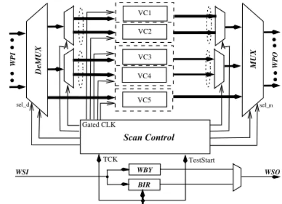
is realized by a two-level MUX-DeMUX pairs. The outer level SMUX-SDeMUXpair is for serial shifting among groups of vir- tual cores while the inner level PMUX-PDeMUX pair for paral- lel shifting within a particular group. Figure 1 illustrates such a power-aware multi-frequency serial-parallel wrapper archi- tecture (MFSP for short). The example IP core contains five virtual cores. They are organized into three groups, each con- sisting of one or several virtual cores. These three groups will enter shift mode in sequence.
VC5 VC4 VC3 VC2 VC1
TestStart TCK
MUXWPI DeMUX
sel_d
WPO
sel_m
Gated CLK
Scan Control
WBY BIR
WSI WSO
Fig. 1.Power-aware serial-parallel wrapper architecture.
Under MFSP architecture, the scan control block is designed that consists of a Capture Finite State Machine, the Clock Di- vision Logic, the on-chip PLL, and a decoder to serialize the shift operation as shown in Figure 2. With reasonable hardware overhead, we realize at-speed test controlling solely on-chip.
Clock Division Decoder Capture FSM
TestStart sel_m
(sel_d) Scan
Gated_clk5 Gated_clk1 Gated_clk2
G1 G2 G3 D1 D2 fc1
fs5 fs4 fs3 fs2 fs1
FM F2 F1 ft
fc5 fc4 fc3 fc2 _en1 _en2Scan
PLL
CPF CPF CPF
CPF CPF
_en5Scan
Fig. 2.Gated multi-frequency shifting.
The Capture FSM is used to generate scan en signals, and control shifting sequence by feeding proper inputs to the de- coder as well as the DeMUX-MUX interface selection signals. The Clock Division Logic is to generate a set of trial frequen- cies F = {F1, F2, ..., FM} which are provided for the virtual cores to be chosen as the shift frequency. In order to simplify the hardware implementation, the ratio of trial frequencies is set as two’s exponent, i.e., FFj
j+1 = 2. The decoder generates the gating signals that will gate off all other shift clocks ex- cept for those in the active group. We use a 2-of-3 decoder here as an example. By setting the combinations of the two in- puts (D2, D1), we may activate one group of virtual cores at a
TABLE I
TEST PARAMETERS FOR COREhCADT01
num ff unc(MHz) Nin Nout Nbi P ow Nsc Lscj
1 200 109 32 72 2572 16 {168 168 166 166 163 163 163 163 162 162 162 162 151 151 151 151}
2 133 144 67 72 450 3 {150 150 150}
3 120 89 8 72 930 10 {93 93 93 93 93 93 93 93 93 93}
4 75 111 31 72 1314 6 {219 219 219 219 219 219}
5 50 117 224 72 2605 5 {521 521 521 521 521}
6 33 146 68 72 576 11 {82 82 82 81 81 81 18 18 17 17 17}
7 25 15 30 72 40 4 {10 10 10 10}
time. For example, when setting (D2, D1)=(0,1), the decoder outputs (G3, G2, G1)=(0,0,1), and only Group − 1 activates and virtual cores V C1and V C2in Group −1 start shifting test data in/out of its wrapper scan chains pulsed at distinct Gated clk1 and Gated clk2 respectively. Similarly by setting (D2, D1)=(1,0) or (1,1), parallel scan-in and scan-out test data for the virtual cores in Group −2 and Group − 3 respectively. When (D2, D1) is set to (0,0), the at-speed clock pulses are applied and the responses are captured. The on-chip functional PLL is reused here to create independent high-speed clock sig- nals used during the capture phase. After serial shifting has fin- ished for the virtual cores, the scanen signals are switched off, and at-speed clock pulses fciare filtered out of gated fsius- ing the clock pulse filters (CPF). The CPF ([24] describes one possible design) replaces clock multiplexer and is controlled simply by the scan en signal.
IV. WRAPPERDESIGNPROBLEMFORMULATION
Without loss of generality, we assume that an embedded IP core C includes Ncvirtual cores V C = {V Ci|i = 1...Nc}, each corresponding to one clock domain. Each virtual core V Ciis given a set of test parameters, e.g., the number of input Nin, output Nout and bidirectional Nbi terminals, the power consumption P ow obtained at the maximum allowable fre- quency Fmax, the number of scan chains Nscand their lengths Lscj. For instance, we show in Table I a representative IP core hCADT01 [21], which is used as a running example through- out this paper. It contains seven virtual cores, divided in terms of different functional frequency. A virtual core V Ci can se- lect a wrapper design wi at certain shift frequency fsi, thus V Ciis expressed as a three-tuple V Ci= {BWi, pi, ti}. Here, BWi = wi×fsi is the bandwidth of V Ci. piis the power of V Ci dissipated at shift frequency fsi, which is computed by pi = P owFmaxi×fsi. ti is the minimum test time obtained at width of wiand shift frequency of fsi, which is calculated by ti= Limaxf (wi)
si ×P , P is the number of test patterns of core C. The power-constrained multi-frequency wrapper design problem (namely, PMWD) can be stated as follows. Given an IP core model C, core bandwidth limitation BWext, and maximum power allowance Pave, select a wrapper design for each virtual core V Ci and determine the corresponding shift frequency fsi such that we minimize the test time for core C while matching the core external bandwidth and satisfying the power constraint at any time.
We define a 3-D bin with the height of test time Tcfor core C, while its length and width are constrained by the external bandwidth BWextand the maximum average power allowance Pave of C respectively. We also define S= {S1, S2, ..., SN}
(N is the number of shelves) as a set of shelves that divide the 3-D bin into N sub-bins. The height of Sj, H(Sj), is defined as the maximum height (or time) among all cubes (or virtual cores) fitted into shelf Si, i.e., H(Sj) = max{ti}, V Ci∈Sj. The virtual cores allocated in the same shelf will perform shift operation simultaneously, i.e., the cubes can overlap in time di- mension. While the cubes within the same shelf cannot overlap to each other along the other two dimensions. It is because two virtual cores cannot share the bandwidth and power if they are tested in parallel. Thus, it is a restricted 3-D bin packing prob- lem. The power dissipation for Sj, given by P(Sj) = ΣMi=1pi,
(M is the number of V Ci∈Sj) should satisfy the power con- straints, i.e., P(Sj) ≤ Pave. The bandwidth for Sj, given by BW(Sj) = ΣMi=1BWi, should match the external bandwidth, i.e., BW(Sj) ≤ BWext. Since the virtual cores within dis- tinct shelves will perform shifting in sequential, the height of the bin, i.e., ΣNj=1H(Sj) is the test time for core C.
Thus, the PMWD problem is deduced into a shelf-packing based 3-D bin design problem where we will minimize the height of the bin bounded by the restricted width and length.
V. PROPOSEDSHELFPACKINGALGORITHM: MWDSP There are three major steps of the proposed MWDSP heuris- tic, namely cube ordering, shelf division and cube packing, and cube merging and shelf elimination. In this section, we give an intuitive description of the steps and illustrate the ap- proaches with the pseudo-code. We start with an initialization step to obtain all candidate rectangle set Ri(wi, Limax) for each virtual core V Ciby running single frequency wrapper config- uration (SFWC). The different combinations of virtual TAM width and maximum wrapper scan chain length, ppi[k]|k ∈ (1...num ppi) = {wi, Limax}, are obtained to provide the flex- ibility to make the trade-off between scan time and test power, thus results in the best selection possible in terms of the con- figuration of the three dimensions of a cube. An important ob- servation from the rectangle set is that doubling the width, the corresponding rectangle area (Ai = wi×Limax) increases or remains the same. This observation has been confirmed with all scan-testable cores in ITC SoC benchmarks [25]. This fur- ther leads to the fact that by halving the shift frequency, the shift time may increase or remain the same when matching the band- width. This feature will be employed to enhance the scheduling efficiency.
Initialization
i1: for each V Ci, i ∈(1...Nc) i2: run SFWC(V Ci);
i3: record ppi[k] := {wk, Lkmax};
Step 1: Cube Ordering
The first step is to provide an ordered cube list to initiate shelf division. We try to find the maximum possible shift frequency fsi for V Ci at which the shift operation is per- formed without exceeding power constraint of core C, i.e., pi(fsi) = fsiF×P owi
max ≤ Pave. Then we find the correspond- ing wrapper design which satisfies the external bandwidth limit while resulting in the minimum test time ti at the maximum possible fsi. Furthermore, with the idea that reducing the shift frequency further (fsi/=2) does not lead to an increase in test time, we take the wrapper design at a lower shift frequency that maintains the same shifting time. In this way, we can save the power consumption significantly by halving the shift fre- quency, and even save the consumed bandwidth BWi (or re- main the same). Thus, we can handle the restrict power con- straint more efficiently by distributing the freed-up power to other cubes so as to pack more cubes into the same shelf.
Cube Ordering 01: for i:=1 to Nc
02: fi nd maximum possible fsisuch that
fsi×P owi Fmax ≤ Pave;
03: wi:=Wtamf ×ft
si ;
04: fi nd closest Pareto point with ppi[j].w ≤ wi; 05: wi:= ppi[j].w;
06: ti:=ppi[j].Lf max
si ;
07: fi nd best wrapper design by fsi/=2 while tiremains the same; 08: sort V Ciin descending order of ti;
09: LV C= {V Ci|i ∈ 1...Nc};
For the given example, we build a list of virtual cores of core hCADT01 in the descending order of their ti min, i.e., Lvc = {V C5, V C1, V C4, V C3, V C2, V C6, V C7,}, un- der the constraints of Wext = 9 and Pave = 4500. We assume that ft=100MHz and a set of trial frequencies F = {100, 50, 25, 12.5} MHz.
Step 2: Shelf Division & Cube Packing
Based on the initial ordering of cubes, we will divide the 3-D bin into several shelves or sub-bins. In this step, we attempt to pack into each shelf as many cubes as possible while satisfying power and bandwidth constraints. The shift operation is per- formed in parallel for the virtual cores in the same shelf while shifting in sequence if allocated within different shelf.
Shelf Division & Cube Packing 11: U nsched:= {LV C}; 12: N :=0;
13: while(|U nsched| ̸= 0)
14: N ++;
15: SN:= {∅};
16: fi nd V Cmaxwith tV Cmax:= maxi∈U nsched{ti}; 17: SN:= SN!{V Cmax};
18: U nsched:= U nsched\{V Cmax}; 19: H(SN) := tV Cmax;
20: compute idle P ow & idle BW ; 21: V Cskip:= {∅};
22: while((|V Cskip| ̸= |U nsched|)
&&(idle BW ̸= 0)&&(idle Pave̸= 0))
23: fi nd V Ctempwith tV Ctemp:= maxi∈U nsched{ti}; 24: if (pV Ctemp> idle P ow)
25: V Cskip:= V Cskip!{V Ctemp};
26: else
27: fi nd maximum possible fsV Ctemp; 28: if (tV Ctemp> H(SN))
29: V Cskip:= V Cskip!{V Ctemp};
30: else
31: fi nd best freq. and wrapper design such that tV Ctempclosest to H(SN);
32: SN:= SN!{V Ctemp};
33: U nsched:= U nsched\{V Ctemp}; 34: update idle P ow & idle BW ;
We follow the order in LV C, and start scheduling from the highest cube (i.e., largest in ti), as their height will dominate the total height of the bin (or the test time for a core). We hope that the resources can be released earlier and more efficiently utilized by smaller virtual cores by scheduling the critical ones earlier. We then divide the bin into shelves by the largest cube in each shelf, i.e., H(Sj) = max{ti} (where V Ciis contained in Sj). After allocating the highest V Cmaxin an empty shelf SN (SN = SN!{V Cmax} and H(SN) = tV Cmax), we try to pack the next highest possible unscheduled cube V Ctempin the same shelf to use up the remaining bandwidth idle BW and power idle P ow. If no suitable cube can be fitted into the idle space or the idle bandwidth/power is used up, a new shelf will be created.
The fast process of checking if a cube can be contained in the shelf is developed by employing the idea that halving the shift frequency may result in an increase in shifting time. Thereby, for the given idleBW , we first check if an incom- ing cube V Ctempcan satisfy the power constraint at the mini- mum frequency (fsV Ctemp = Fmin), i.e., it cannot be allocated in the shelf if pV Ctemp(fsV Ctemp) > idle P ow. If it satisfies power limit, we further check if V Ctemp can meet the height allowance at the maximum frequency (fsV Ctemp = fsmax
V Ctemp),
i.e., it cannot be contained if tV Ctemp > H(SN), where tV Ctemp is the time for V Ctemp at fsmax
V Ctemp. If it satisfies, V Ctempwill be allocated. Since the cube meets the bandwidth and power constraints, we will pick the best frequency within the range (Fmin, fsmax
V Ctemp) such that its height is closest to H(SN) while tV Ctemp≤H(SN). The reason is simply to free up more bandwidth and power so as to contain more smaller virtual cores next.
After step 2, we obtain the initial schedule of the virtual cores of core hCADT01 as shown in Figure 3 and the total test time is TC=12.71.
900
600 300
S5 S4 S3
S2
S1
1.68 87.5
0.891.51.863.255.21 5
VC_7, p7=5
12.71
600
VC_5, p5=2605 VC_4, p4=657
VC_1, p1=2572 VC_3, p3=465 VC_2, p2=450
VC_6, p6=576 900
500
Fig. 3.The illustration of step 2 applied to hCADT01.
Step 3: Cube Merging & Shelf Elimination
We have divided the bin into N shelves and sorted their heights in descending order after step 2. Each shelf contains one or more cubes in decreasing order of height. We further reduce the height of the bin in step 3 by merging the cubes in shelf Sj into Si such that H(Si new) + H(Si new) <
H(Si) + H(Sj). If all cubes in Sj can be merged into Si, Sjis eliminated.
We use the following example to illustrate the basic idea. Assuming a merging candidate shelftwocontains two cubes, V Ctwoand V Ctempas shown in Figure 4(a). We try to merge the cubes into shelfoneto further reduce the hight of bin. We first check if the power constraint can be satisfied when adding V Ctwo into shelfone, i.e., pV Ctwo ≤ rem P ow. Again, the maximum possible frequency is obtained in order to achieve a minimum testing time under bandwidth constraint. If meeting the power constraint, we try to free up the width of V Cone
while keeping its height tV Cone < Hmerge. In this way, more bandwidth could be distributed to V Ctwowith its height tV Ctwo < Hmerge. In the meantime, the freed-up bandwidth and power could be efficiently utilized by V Ctempin shelftwo
to further reduce the height of shelftwo. V Ctwocan be merged into shelfone only if the sum of the height of the two new shelves reduces, i.e., Hnew(Shelfone) + Hnew(Shelftwo) < Hmergeas shown in Figure 4(b).
Cube Merging & Shelf Elimination 41: U nmerged:= {Si|i ∈ 2...N }; 42: Smark:= Smark!S1;
43: while(|Smark| ̸= |U nmerged| + 1)
44: fi nd Shelfonewith H(Shelfone) := maxi∈U nmerged{H(Si)}; 45: fi nd V Conewith tV Cone:= maxi∈Shelfone{ti};
46: Shelf skip:= Smark!{Shelfone}; 47: while(|Shelf skip| ̸= |U nmerged| + 1) 48: fi nd Shelftwowith
H(Shelftwo) := maxi∈U nmerged\Shelf skip{H(Si)}; 49: fi nd V Ctwowith tV Ctwo:= maxi∈Shelftwo{ti}; 50: Hmerge:= H(Shelfone) + H(Shelf two); 51: compute idle power rem P ow in Shelfone; 52: if (pV Ctwo> rem P ow)
53: Shelf skip:= Shelf skip!{Shelftwo};
54: else
55: V Conerelease rem BW such that tV Cone< Hmerge& V Ctwofi t into Shelfonewith tV Ctwo< Hmerge; 56: fi ndV Ctempwith tV Ctemp:= maxi∈Shelftwo\V Ctwo{ti}; 57: redistribute released try BW and try P ow to V Ctemp; 58: if (Hnew(Shelfone) + Hnew(Shelftwo) < Hmerge) 59: record V Cone, V Ctwo, and V Ctempwrapper design; 60: Shelfone:= Shelfone!{V Ctwo};
61: Shelftwo:= Shelftwo\{V Ctwo}; 62: if (Shelf two== ∅)
63: U nmerged:= U nmerged\{Shelftwo};
64: else
65: Shelf skip:= Shelf skip!{Shelftwo}; 66: if Shelfonecannot be merged with any shelf 67: Smark:= Smark!{Shelfone};
two Hmerge
VCtemp
VCone VC two
(b) VC is merged into Shelfonetwo
H(Shelf)
VCone
VCtwo VC temp
H(Shelf)oneH(Shelf)two Hmerge
(a) Before merging
H(Shelf)one
Fig. 4.An example on merging a cube into a shelf hCADT01.
The final packing of cubes is illustrated in Figure 5. As we can see, the total height of bin is reduced from 12.71 to 11.83 by applying step 3. With the schedule result, we obtain the minimum shifting time for core hCADT01 as well as the mul- tiple frequency assignment among the virtual cores. The cor- responding wrapper architecture design is thus determined in Figure 6.
4.79 3.72
VC_3, p3=930 300
1.67 400
VC_2, p2=450
1.62 500
VC_6, p6=576
0.16 VC_7, p7=40 900
S2 S3 S4
11.83
600
VC_5, p5=2605 VC_4, p4=657
600 300
S1 5.21 5
VC_1, p1=2572
Fig. 5.The illustration of step 3 applied to hCADT01.
sel_m sel_d
DeMUX
TCK
MUX
TestStart Scan Control
WPO
Gated CLK VC6
VC7 VC2 VC3 VC
VC5 VC4
1
WPI
Fig. 6.Multi-frequency wrapper architecture for core hCADT01.
VI. SIMULATIONSTUDY
We evaluate the proposed multi-frequency wrapper design with shelf packing algorithm MWDSP via simulation and com- pare the test time with the best published approach. Since none of the public domain SoC benchmarks provides multi- ple frequency information of the embedded cores, we will use the same hypothetical but nontrivial multi-frequency IP core, hCADT01 (given in Table I), for simulation and comparison. Assuming that the ATE will shift test data at ft = 100HM z which is synchronized to a division of the maximum functional frequency of core hCADT01. Given a set of trial frequencies F = {100, 50, 25, 12.5}M Hz (use the same set for fair com- parison to [21]).
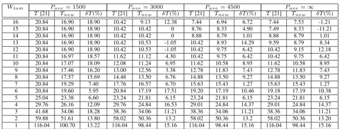
Table II shows the test application time of hCADT01, Tnew
(in µsec) using MWDSP algorithm with the consideration of a wide range of external width Wtamand various power con- straints Pave. The test time reported in [21] is also listed for comparison. The percentage improvement of Tnewover T [21] is calculated as δT = T[10]−TT[10]new. As observed from Table II, the MWDSP approach outperforms the existing best approach. The reduction in the overall shifting time can reach as high as 18.9%.
The advantage of our proposed multi-frequency serial- parallel shifting architecture (MFSP) is that we try to relax the power constraint by serializing shifting. If only some of the vir- tual cores will shift in parallel at a particular time slot, these vir- tual cores can shift at a higher frequency while satisfying power constraint. In the meantime, overall bandwidth could be dis- tributed only among these cubes to achieve a minimum shifting time. From the comparison to [21], we observe that when the power constraint is quite tight, our approach achieves more im- provement by serializing the shift operation. Even when there is no power constraint (i.e., pave = ∞), our approach can re- duce the shift time further by parallelizing the shifting. The shelf packing based optimization technique provides the flexi-
TABLE II
COMPARISON RESULTS FOR COREhCADT01
Wtam Pave= 1500 Pave= 3000 Pave= 4500 Pave= ∞
T [21] Tnew δT (%) T [21] Tnew δT (%) T [21] Tnew δT (%) T [21] Tnew δT (%)
16 20.84 16.90 18.90 10.42 9.13 12.38 7.44 6.94 6.72 7.44 7.53 -1.21
15 20.84 16.90 18.90 10.42 10.42 0 8.76 8.33 4.90 7.49 8.33 -11.21
14 20.84 16.90 18.90 10.42 10.42 0 8.88 8.79 1.01 8.88 8.79 1.01
13 20.84 16.90 18.90 10.42 10.53 -1.05 10.42 8.93 14.29 9.59 8.79 8.34
12 20.84 16.90 18.90 10.42 10.53 -1.05 10.42 9.75 6.42 10.42 9.15 12.18
11 20.84 16.97 18.57 11.62 11.12 4.30 10.42 9.75 6.42 10.42 9.75 6.42
10 20.84 17.07 18.09 12.08 11.24 6.95 11.62 10.58 8.95 11.62 10.58 8.95
9 20.84 17.46 16.20 13.00 12.56 3.38 12.78 11.83 7.43 12.78 11.83 7.43
8 20.84 17.57 15.69 14.48 13.50 6.76 14.88 13.50 9.27 14.88 13.50 9.27
7 20.84 19.29 7.40 17.76 16.57 6.70 15.63 15.43 1.27 15.63 15.43 1.27
6 20.84 19.60 5.95 20.84 17.19 17.51 19.20 17.19 10.46 19.18 17.19 10.38
5 25.04 23.38 6.60 23.24 21.81 6.15 23.24 21.81 6.15 23.24 21.81 6.15
4 29.76 26.16 12.09 29.76 24.84 16.53 29.01 24.84 14.37 29.01 24.84 14.37
3 41.68 34.06 18.28 38.36 34.06 11.21 38.36 34.06 11.21 38.36 34.06 11.21
2 59.88 51.61 13.80 58.02 50.36 13.2 58.02 50.36 13.2 58.02 50.36 13.20
1 116.04 100.70 13.22 116.04 98.44 15.16 116.04 98.44 15.16 116.04 98.44 15.16
bility to configure the wrapper into a serial architecture when the power and bandwidth constraints are tight, while transform to a parallel architecture when the constraints become loose. As the test time and test power of a scan-testable core are inter- dependent (e.g., the scan time is inversely proportional to the scan frequency, while the test power increases when increasing the scan frequency), we can achieve the best trade-off in a way that power-critical virtual cores will be serialized in shifting while others are accommodated in parallel with them to reduce the overall test time while meeting the bandwidth limit.
VII. CONCLUSION
We have presented in this paper a novel power-aware serial- parallel wrapper architecture for multi-frequency IP modules. The tight power budget is handled by gating off certain virtual cores at a time to gain the best trade-off between test power and scan time. We have formulated the power-constrained multi- frequency wrapper optimization problem into a 3-D Bin Pack- ing problem and proposed an efficient shelf-packing heuristic algorithm to optimize the wrapper scan architecture and mini- mize the test time of a core. Through performance evaluation, our approach outperforms those previously published. The im- provement can reach as high as 18.9%. The algorithm requires a negligible amount of computation time (6ms) and therefore is suitable for more complex cores. This is especially an im- provement over the CPU-intensive ILP-based method in [21].
REFERENCES
[1] T. Waayers, E. J. Marinissen, and M. Lousberg, “IEEE std 1500 com- pliant infrastructure for modular SOC testing,” in Proc. of ATS, p. 450, November 2005.
[2] Y. Zorian, E. J. Marinissen, and S. Dey, “Testing embedded-core-based system chips,” IEEE Computer, vol. 32, pp. 52–60, June 1999. [3] E. J. Marinissen, S. K. Goel, and M. Lousberg, “Wrapper design for em-
bedded core test,” in Proc. of ITC, pp. 911–920, october 2000. [4] S. Koranne, “A novel reconfi gurable wrapper for testing of embedded
core-based SoCs and its associated scheduling algorithm,” Journal of Electronic Testing: Theory and Applications, vol. 18, pp. 415–434, Au- gust 2002.
[5] V. Iyengar, K. Chakrabarty, and E. J. Marinissen, “Co-optimization of test wrapper and test access architecture for embedded cores,” Journal of Electronic Testing: Theory and Applications, vol. 18, pp. 213–230, April 2002.
[6] Y. Huang and et.al, “Optimal core wrapper width selection and SOC test scheduling based on 3-D bin packing algorithm,” in Proc. of ITC, pp. 74– 82, 2002.
[7] S. K. Goel, “An improved wrapper architecture for parallel testing of hierarchical cores,” in Proc. of ETS, pp. 147–152, May 2004.
[8] B. Vermeulen, S. Oostdijk, and F. Bouwman, “Test and debug strategy of the PNX8525 NexperiaTM digital video platform system chip,” in Proc. of ITC, pp. 121–130, October 2001.
[9] M. Amodeo and B. Cory, “Beyond at-speed,” in Test and Measurement World, pp. 43–48, November 2005.
[10] N. Tendolkar and et.al, “Scan-based at-speed testing for the fastest chips,” 2001. Mentor Graphics White Paper.
[11] P. Varma and S. Bhatia, “A structured test reuse methodology for core- based system chips,” in Proc. of ITC, pp. 294–302, October 1998. [12] A. Hales and E. Marinissen, “IEEE P1500 web site.”
http://grouper.ieee.org/groups/1500.
[13] J. Aerts and E. J. Marinissen, “Scan chain design for test time reduction in core-based ICs,” in Proc. of ITC, pp. 448–457, 1998.
[14] E. J. Marinissen, R. Arendsen, G. Bos, H. Dingemanse, M. Lousberg, and C. Wouters, “A structured and scalable mechanism for test access to embedded reusable cores,” in Proc. of ITC, pp. 284–293, 1998. [15] G. Hetherington and et.al, “Logic BIST for large industrial designs: Real
issues and case studies,” in Proc. of ITC, pp. 358–367, 1999.
[16] L.-T. Wang, X. Wen, P.-C. Hsu, S. Wu, and J. Guo, “At-speed logic bist architecture for multi-clock designs,” in Proc. of ICCD, pp. 475–478, 2005.
[17] A. Khoche, “Test resource partitioning for scan architecture using band- width matching,” in Digest of Int’l Workshop on Test Resource Partition- ing, pp. 1.4.1–1.4.8, 2001.
[18] A. Sehgal and et.al, “Test cost reduction for SoCs using virtual tams and lagrange multipliers,” in Proc. of DAC, pp. 738–743, June 2003. [19] Q. Xu and N. Nicolici, “Multi-frequency test access mechanism design
for modular SOC testing,” in Proc. of ATS, pp. 2–7, November 2004. [20] T. Yoneda, K. Masuda, and H. Fujiwara, “Power-constrained test
scheduling for multi-clock domain socs,” in proc. of DATE, 2005. [21] Q. Xu, N. Nicolici, and K. Chakrabarty, “Multi-frequency wrapper de-
sign and optimization for embedded cores under average power con- straints,” in proc. of DAC, June 2005.
[22] L. Whetsel, “Adapting scan architectures for low power operation,” in Proc. of ITC, pp. 863–872, October 2000.
[23] J. Sexena, K. Butler, and L. Whetsel, “An analysis of power reduction techniques in scan testing,” in Proc. of ITC, pp. 670–677, October 2001. [24] M. Beck, O. Barondeau, M. Kaibel, F. Poehl, X. Lin, and R. Press, “Logic
design for on-chip test clock generation - implementation details and im- pact on delay test quality,” in Proc. of DATE, pp. 56–61, 2005. [25] E. J. Marinissen, V. Iyengar, and K. Chakrabarty, “ITC’02 SOC test
benchmarks.” http://www.hitech-projects.com/itc02socbenchm/.