Paper 21.1 INTERNATIONAL TEST CONFERENCE 1
978-1-4244-7207-9/10/$26.00 © 2010 IEEE
Constrained ATPG for Functional RTL Circuits Using F-Scan
Marie Engelene J. Obien, Satoshi Ohtake and Hideo Fujiwara
Graduate School of Information Science, Nara Institute of Science and Technology
Kansai Science City 630-0192, Japan, {obien-j, ohtake, fujiwara}@is.naist.jp
Abstract
In this paper, we present an approach to constrained automatic test pattern generation (ATPG) for functional circuits at register-transfer level (RTL) with the help of a design-for-testability (DFT) technique called F-scan. The DFT method optimally utilizes existing functional elements and paths for test, thus it effectively reduces the hardware overhead due to test. This is done by arranging all registers in the circuit into F-scan-paths and augmenting necessary circuitry at RTL. After DFT, we create the constraint test generation model of the circuit based on the test environment obtained from the information of F-scan- paths. With this approach, only the applicable test vectors to the F-scan-paths can be generated and test application time is kept at the minimum. The comparison of F-scan with the performance of gate-level full scan design is shown through the experimental results.
1. Introduction
In order to increase the testability of a circuit, design for testability (DFT) is the most popular approach. Scan design is the mainstream technique used today because it effectively addresses the complexity of test pattern generation. The trade-offs of full scan, however, prove DFT to be very costly in terms of hardware overhead and test application time. Moreover, scan-based DFT methods may change the circuit states during test mode, which can possibly make them different from that in functional mode. This means that ATPG tools may generate scan patterns that are illegal during functional mode, hence result in over-testing.
We have proposed F-scan in [18, 19], which improves full scan design in terms of area overhead and scan time. F- scan organizes every register in the circuit in an F-scan- path by maximizing the use of available functional logic and paths to be used for F-scan, hence keeping hardware overhead due to test at the minimum. Moreover, single F- scan-paths automatically allow parallel and simultaneous scan (dependent on the bit width), thus minimizing test application time as well. For further reduction, we also prioritize the use of multiple F-scan-paths, whenever readily available (dependent on the available primary inputs and outputs). In this paper, we complete the method by proposing a constrained ATPG method that ensures
high fault coverage. We describe the methodology of our constrained ATPG approach in this paper.
An inherent feature of the constrained ATPG we propose here is the ability to generate test patterns that are functionally reachable states as much as possible. In this case, there is a possibility to prevent over-testing. This idea can be related to pseudo-functional scan testing, which has been proposed [20-26] to address the problems of scan tests. In this technique, any test pattern that is scanned-in conforms “closely” to a functionally-reachable state. The idea is that if the scanned state is functionally reachable, then that part of the circuit during test operates almost similarly with its normal mode. This way, over- testing and yield loss problems can be reduced [20]. Pseudo-functional scan test depends on the ability to identify reachable or unreachable states before ATPG. Our approach, however, is a constraint-based ATPG technique that tries to generate legal test patterns as much as possible. If this method is applied on the circuit with complete justification and propagation environment during test without any changes on the functional elements and paths, we can assure that all test patterns are legal. Our algorithm for F-scan proposed in [18, 19] aims for high fault coverage with the least area overhead possible. This is done by utilizing the available functional elements and paths for testing as much as possible, thus the circuit generally works close to normal mode during testing. Thus, as high fault coverage is achieved with F-scan, there can also be a possibility of reducing over-testing. For this study, we focus on ATPG for stuck-at-fault model, but, path-delay faults and transition faults may also be tested using our approach.
The rest of the paper is organized as follows. Section 2 summarizes our F-scan design method. In section 3, we explain the test environment generation. We provide the methodology for constrained ATPG in section 4. Experimental results are given in section 5. We briefly discuss the feasibility of using F-scan to practical designs. Finally, this paper is concluded in section 7.
2. F-Scan
In this section, we first provide the works related to F-scan design. Then, we give a brief introduction about assignment decision diagrams and the nine symbol algebra
Paper 21.1 INTERNATIONAL TEST CONFERENCE 2
used for test environment generation. Finally, we briefly describe F-scan concepts such as essential value justification, essential error propagation, F-path, F-scan- path, F-scannable circuit, and the DFT selection method.
2.1 Related Works
Several DFT techniques at RTL have been proposed, most are scan-based. Gupta et al. [3] introduced a structured partial scan design that converts only the selected flip-flops into scan flip-flops. H-Scan [4],[6] uses paths between registers, but only through multiplexers. Orthogonal scan [5] uses data path flow as scan path. Huang et al. [7] provided an effective approach for RTL scan by arranging registers in scan chains through cost rules, which ensure the lowest possible area overhead for the circuit. D-scan [8] uses thru functions (logic that allow values to pass through hardware modules) with predetermined control signals for scan paths in the circuit. These techniques are scan-based methods that try to utilize available circuitry for test. However, further reduction to area overhead can still be achieved, as proven by our proposed method in [18, 19]. Aside from reduced area overhead, test application is also kept at the minimum by F-scan because of limited use of hold functions. Using hold functions does not only increase the number of primary inputs augmented, but also results in multiple test configuration.
Non-scan DFT methods at RTL were also proposed [10],[12-15]. These approaches, however, require a test controller to be added to the circuit. Moreover, the said methods are applicable to structural description of circuits, while our method can handle functional RTL. F-scan deals with the circuit in assignment decision diagrams (ADD), which represent both the controller and data path parts uniformly. Thus, the application of both the DFT method and test is consistent for the entire circuit. The use of ADD also allows for easier manipulation of the circuit for DFT.
2.2 Unified Circuit Representation and the Nine Symbol Algebra
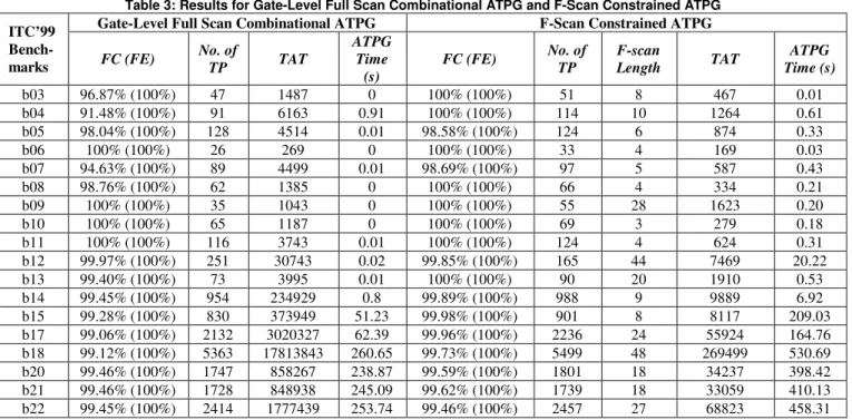
There have already been works on test generation using Assignment Decision Diagram (ADD) shown in Fig. 1 [17, 27]. ADD is a representation developed for high-level synthesis that is complete, efficient, and partially unique. It can be used to describe structural or functional RTL
circuits in which the controller part and the data path part are consistently represented.
ADD is an acyclic graph presented in [16], which consists of four parts: 1) the assignment value; 2) the assignment condition; 3) the assignment decision; and 4) the assignment target. There are four types of nodes used to implement it: a) read nodes and b) write nodes, c) operation nodes, and d) assignment decision nodes or ADN. The read nodes represent the current contents of the input ports, registers, and constants. The write nodes contain the values assumed by the read nodes in the next clock cycle. They also represent primary outputs. The operation nodes represent arithmetic and logic operations and the ADNs select from a set of values that are provided to them, similar to multiplexers.
In [17], an RTL-ATPG algorithm is proposed using ADD as its data structure and a nine-valued algebra for justification and propagation. [27], on the other hand, presented a SAT-based methodology for test generation. Their algorithm exploits the implication-based ADD representation to provide a unified framework for the testability analysis of RTL circuits. Our approach, however, uses ADD represented RTL circuits for DFT and test generation. Using ADD, it is easier to analyze and manipulate the circuit for F-scan.
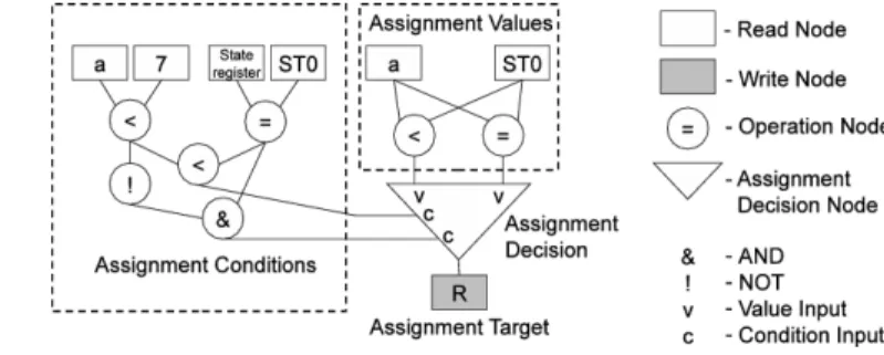
The concept of functional scan uses the following nine symbol algebra used by Ghosh [17] for automatic test pattern generation (ATPG) of ADD circuits.
1. Cg (general controllability) of a register means it can be controlled to any arbitrary value.
2. Cq (controllability to a constant) of a register means it is controllable to any fixed constant value. This subsumes C0 (controllability to zero), C1 (controllability to one), and Ca1 (controllability to all one).
3. O (observability) of an RTL variable is the ability to observe fault at a variable.
4. Cs (controllability to a state) is similar to Cq but is applied to state registers to control to a particular state.
5. Other symbols are Cz (controllability to the Z value) and O’ (complement observability), but these are not used for our study.
RTL Code:
xe_01 := a < 7;
xe_02 := (State_register = ST0);
if (xe_01 < xe_02) then R = a < ST0;
else if ((not xe_01) and xe_02) then R = (a = ST0);
Figure 1. The assignment decision diagram.
Paper 21.1 INTERNATIONAL TEST CONFERENCE 3
In Figure 2, F-scan is illustrated with the use of these symbols.
2.3 F-Scan Definitions
We introduced the concepts of functional scan in [18, 19]. In Figure 2, we see that any arbitrary value can be controlled and observed through operation nodes and ADN. By controlling the other inputs (side inputs) of an operation node or ADNs to Cq, Cg and O can be achieved for that node.
Figure 2. a) General controllability and b) observability of operation nodes and ADNs.
Figure 3. a) Essential value justification and b) Essential error propagation.
Figure 3 illustrates essential value justification and essential error propagation. Let us assume a path p(X, Y) from a read node to a write node such that the side inputs of operational nodes and control inputs of ADNs can be controlled to fixed constants. We have an essential value set of Y such that it is a set of values that can be assigned to Y according to the functional description of p. Then, essential value justification for p(X,Y) means that any value in the essential value set of Y can be justified at Y by p(X,Y) provided that any value in the essential value set of X is justified at X. Similarly, we have an essential error set of X such that it is a set of errors that can be detectable from X. Then, essential error propagation for p(X,Y) means that any error in the essential error set of X can be propagated to Y by p(X,Y).
Functional scan or F-scan, therefore, is satisfied when both essential value justification and essential error propagation can be done for all registers in the circuit. This is done by including all registers in F-scan-paths. To discuss F-scan-paths, we defined F-paths in [19], which represents the topology of a path in an ADD circuit from a read node to a write node. We have three cases for p(X,Y) to be considered an essential F-path.
1. X and Y are both registers: p(X,Y) satisfies both essential value justification and essential error propagation.
2. X is a PI: p(X,Y) satisfies essential value justification. 3. Y is a PO: p(X,Y) satisfies essential error propaga-
tion.
From the definition of F-path, F-scan-path is then the concatenation of F-paths wherein the head is a PI and the tail is a PO.
Aside from essential value justification and essential error propagation, complete value justification and complete error propagation are also considered. That is, any value or error can be justified or propagated along the path. Thus, an F-scan-path can be a concatenation of a) essential, b) complete, or c) essential and complete F-paths.
In order to make an ADD circuit F-scannable, every register should be included in an F-scan-path, wherein it appears just once.
Figure 4. Essential F-path: a) X and Y are registers, b) X is PI, and c) Y is PO.
2.4 F-Scan DFT Method
The DFT algorithm consists of the following general stages. Stage 1. Determine all possible F-paths exhaustively
based on the ADD circuit.
Stage 2. Construct the F-scan-paths to make the circuit F-scannable.
We have described in [19] the method to ensure the least area overhead possible in constructing F-scan-paths. We have also provided a local optimum heuristic approach to simplify the algorithm of identifying F-paths and disjoint F-scan-paths. We used hold function exclusively to handle state registers that cannot be included in any F-scan-path. We also proposed new ADD elements for masking in order to control the operation nodes with side inputs that are not readily constants. The resulting area overhead of F-scan is compared with gate-level full scan in our experimental results.
Another point of discussion with F-scan is its possible effect on logic synthesis. F-scan may introduce some extra data flow at the ADD level and some operations may be involved in the additional data flow. Consequently, this may prevent sharing of one operational module (at structural RTL) with other several operations (at functional RTL). If so, the gate-level circuit after synthesis may be very large. However, our experimental results show that this does not occur.
Paper 21.1 INTERNATIONAL TEST CONFERENCE 4
Figure 5. An illustration of test environment generation by example.
3. Test Environment Generation
Test environment is generated for each of the F-scan-paths in the circuit in order to do testing. Each F-scan-path has a schedule of scan-in and –out for every register included in the path depending on the order of these registers along the F-scan-path. The F-scan-paths are also activated using control signals (scan and hold, if necessary). Thus, the test environment for the entire circuit-under-test (CUT) consists of the scheduled signal assignment values and output response involved to complete an F-scan cycle. This is illustrated in Figure 5.
The test environment involves three phases: a) F-scan-in, b) test, and c) F-scan-out. After the first F-scan-in, both F- scan-in and F-scan-out are overlapped.
1. F-scan-in phase. In this phase, all read nodes used to transfer values must contain the corresponding test pattern obtained during ATPG. The read nodes that activate the F- scan-path should be activated with the necessary values, e.g. 1 or 0 for scan/hold pin and initialize pin. Since the test patterns are yet to be embedded, the F-scan-in environment includes the schedule of signal assignments that completes the F-scan-in phase. Once ATPG is done, the inputs to the PIs involved during test are obtained by generating the test sequence. The input test vectors included in the test sequence consists of the test patterns embedded to the F-scan-in test environment and the signals that activate F-scan. F-scan-in phase completes one cycle when all registers are scanned-in with test vectors. Since the method of generating the patterns uses constrained
*C0 is a new ADD element that describes a C0 mask function. When the test pin is set to 0, the output of this element is equal to In1. If the test pin is set to 1, the output of this element is equal to 0. The new mask elements are proposed in [19], which are saved in the library.
This is the complete cycle of F-scan on Circuit E. At t0, the value of In1 goes to X. At t1, the value of X goes to Y while a new value goes to X from In1. At this point, all registers have been scanned-in. At t2, the circuit goes to normal mode. From t3 to t4, the X and Y are scanned-out.
Paper 21.1 INTERNATIONAL TEST CONFERENCE 5
ATPG, only valid patterns are embedded into the test sequence, thus all patterns are guaranteed to be scanned-in through F-scan-paths.
2. Test phase. This phase happens by deactivating the scan mode and switching the circuit to normal mode. In this phase, all registers are used as input-registers (read nodes) and the same registers (write nodes) are used as output-registers for testing the circuit. The test-mode environment includes the PI values (if necessary), the output response, and the scan/hold/initialization pin assignment that will turn the circuit to normal mode, i.e. zero value.
3. F-scan-out phase. As stated previously, both the F- scan-in phase and F-scan-out-phase are overlapped after the first scan-in. Hence, the signals that activate F-scan-in also enable F-scan-out at the same time, which is illustrated in Figure 5(d).
In F-scan-out phase, the values in all registers are scanned- out. In order to check all the register values obtained after test phase for faults, the test response of this phase is compared with the generated expected response (constrained ATPG). Since the method of generating the expected test responses uses constrained ATPG, only valid output values are embedded into the test response sequence. Moreover, since the constraint is based on the test environment of the F-scan-path, even if the F-paths are not I-paths (or complete F-paths), the test response during this phase does not need to be adjusted before comparing it with the expected response. I-paths or identity-paths are paths that are enabled by switching some pins such that data can be transmitted through them unchanged. The concept of I-paths has been defined in [30]. The adjustment is inherent to the constrained ATPG. The F- scan-out environment therefore is the same with the F- scan-in environment, only it includes the activation of paths to POs as well. One cycle of F-scan-out phase is completed when all values in the registers are scanned-out to the POs.
Sample Case. An example is given in Figure 5, which illustrates the generation of the test environment and the test sequence. The original circuit, E (without augmentation), is shown in Figure 5(a). The state register and the control values to the ADNs are not shown, and so these are not included in the example’s test environment. Figure 5(b) shows the F-scannable circuit E. The F-paths are indicated as bold lines and the mask is presented as a C0 element. The test environment is given by Figure 5(c), wherein it shows that a complete scan cycle is equal to five clock cycles, t0 to t4. Figure 5(d) gives the test environment and the resulting test sequence given the test patterns TP1 and TP2 and test responses TR1 and TR2. Shown in the test sequence, the first F-scan-in occupies t0 and t1. Test phase happens in t2. From t3 to t4, F-scan-in and F-scan-out are overlapped. The same goes on until all
the members of the set of test patterns generated by ATPG are embedded with the test environment into the test sequence.
For our method, the test patterns are generated using a combinational ATPG engine on the synthesized F- scannable circuit with constraints. The method of embedding constraints during ATPG is described in the next section. Subsequently, the test sequence is derived by embedding the test patterns to the test environment. The test sequence includes both input test vectors and test response generated using the constrained ATPG.
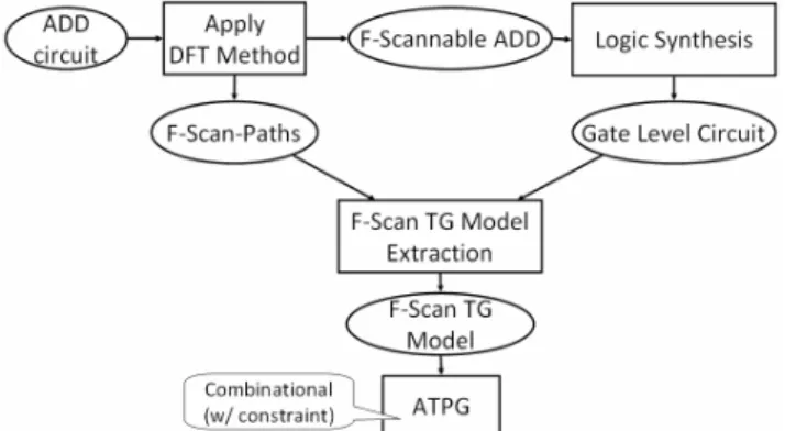
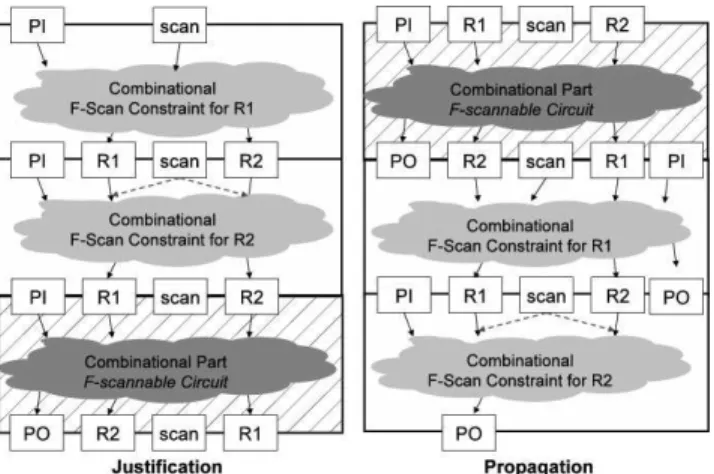
4. Constrained ATPG
Most of the works on constrained ATPG first determine legal or illegal states and then, feed these constraints to the ATPG tool. Our approach, however, embeds the constraints on the combinational gate-level circuit by creating the F-scan test generation model before ATPG.
Figure 6. Flow of F-scan methodology until ATPG.
The F-scan test generation model (FTGM) is based on the test environment generated for the F-scannable ADD circuit. The extraction of FTGM is summarized as follows:
1. Create combinational F-scan constraint module for each flip-flop in the ADD circuit that will allow both F-scan-in and F-scan-out.
2. Connect the combinational F-scan constraint modules to the synthesized F-scannable ADD circuit according to the schedule in the test environment.
The creation of F-scan constraint module and its connection with the synthesized F-scannable ADD circuit are further discussed in the next subsections. Figure 7 illustrates FTGM in a similar manner we discussed the test environment in Figure 5(c). Using FTGM during combinational ATPG, we control the signals that activate the F-scan-paths by adding PI constraints (1 for scan and 0 for reset). This way, the ATPG engine generate test patterns considering the F-scan-paths activated, thus, all test patterns and responses generated are guaranteed to be justifiable and propagable through F-scan-paths. Since the F-scan-paths utilize available functional elements and paths
Paper 21.1 INTERNATIONAL TEST CONFERENCE 6
in the circuit, the set of test patterns generated is within the functionally-reachable space of the circuit. In effect, occurrence of redundant faults is reduced and fault coverage is increased. Moreover, despite the high fault coverage expected with this method, over-testing is also dealt with because the constrained ATPG generates legal test patterns.
Figure 7. F-scan Test Generation Model illustrated.
4.1 F-scan Constraint Module
After logic synthesis, we extract the combinational part of the gate-level circuit by converting all flip-flops into pseudo-primary inputs (PPIs) and pseudo-primary outputs (PPOs). This way, combinational ATPG may be applied, of which the testability is that of full scan design. Our approach, however, connects these PPIs and PPOs with the F-scan constraint modules before applying combinational ATPG.
The F-scan constraint module for each flip-flop is obtained from the combinational F-scannable circuit using the following steps:
1. Determine which F-scan-path the flip-flop belongs to. The F-scan constraint module will depend on the test environment of the F-scan-path that includes the flip- flop.
2. Each F-scan constraint submodule includes the F-path from a PI or register to a PO or another register. Thus, the first F-scan constraint submodule contains the combinational part that includes the path which connects the PI of the F-scan-path to the next register (according to the order of registers in the F-scan-path). Subsequently, the last F-scan constraint submodule includes the path which connects the last register in the F-scan-path to the PO. Thus, the number of F- scan constraint submodules for a flip-flop corresponds to the F-scan-path length. The creation of an F-scan constraint submodule is done by using the same combinational gate-level circuit, but activating only the F-scan-path that includes the flip- flop (adding PI constraints to control inputs scan and
reset). This way, only the combinational part of the involved F-path is extracted.
3. When all of the F-scan constraint submodules are created, they are connected together according to the test environment. With the connection of the submodules, we have the F-scan constraint module for justification and propagation for a flip-flop. As an example, for the F-scannable Circuit E in Figure 5, we have the following order of registers and PI/PO in the F-scan-path: In 1 X Y Out. So, if all of the PI/PO and registers are 1-bit and we are to create the F-scan constraint module for X, the first F-scan constraint submodule includes the path In 1 X. Then, since this submodule already ends in X, it is already considered as the F-scan constraint module for justification of X. This constraint module is then connected to the PPI of the combinational circuit corresponding to X. Similarly, the propagation F- scan constraint module has the following submodules: X Y and Y out. The PPO of the combinational circuit corresponding to X is connected to the submodule X Y. This submodule is then connected to the PPO of the submodule Y out corresponding to Y.
The creation of the F-scan constraint modules allows combinational ATPG to be used to generate test patterns for all kinds of fault models. For this study, we provide results for stuck-at-fault model. During experiment, since the combinational ATPG is done on the circuit with F-scan constraints, the fault coverage achieved by the ATPG tool is already the real fault coverage of the test pattern for the circuit. This means that the test pattern generated at gate- level automatically achieves the same coverage as when it is applied on ADD level, due to the constraint modules. Thus, there is no need for fault simulation.
4.2 Detection of Redundant Faults
For full scan, ATPG can identify all combinational redundancies, which are not tested. However, all sequential redundant faults in the original circuit become testable after full scan design. Thus, the ATPG have to generate test patterns for those testable faults that were redundant before DFT. That is, over testing. On the other hand, some combinational redundancies may be included in the test domain of constrained ATPG for F-scan. This is because F-scan may have added logic that will allow these redundant faults to be testable, since the DFT aims for high fault coverage. However, some sequential redundancies may be identified to be redundant for F-scan constrained ATPG and escaped for testing. This means that, the more that the circuit mainly uses functional elements and paths during test, the more redundancies can be identified by the constrained ATPG. This, in return, produces lower fault coverage.
Paper 21.1 INTERNATIONAL TEST CONFERENCE 7
4.3 Testing F-scan-paths
It is necessary to test the F-scan-paths to ensure that the scan-in data can be justified to all registers correctly and the errors can propagate along these paths without masking. From the heuristic algorithm used to create F-scan-paths in [19], all possible errors can be propagated along F-scan- paths. Hence, testing F-scan-paths can be done by scanning-in and –out test patterns without switching to normal mode, which can be done at operational speed. By doing so, the errors can be checked if there is any value in the scanned-out data that is not expected. If there are no errors in this test, error masking will never happen and the F-scanned-in values are always correct.
5. Experimental Results
For our experiments, we have applied F-scan to 20 ITC’99 Benchmark Circuits. The original functions of the circuits are given in Table 1. This information show the variety of circuits involved in the experiments in terms of function. This proves that F-scan is applicable to any circuit that can be described at functional RTL (ADD) and any functional path between registers can be used given that it satisfies essential value justification and essential error propagation.
Table 1: Original Functions of the Circuits [28] Circuit Original Function
b01 Finite state machine (FSM) comparing serial flows b02 FSM with binary coded decimal number recognition b03 Resource arbiter
b04 Compute minimum and maximum b05 Elaborate contents of a memory b06 Interrupt handler
b07 Count points on a straight line
b08 Find inclusions in sequences of numbers b09 Serial-to-serial converter
b10 Voting system
b11 Scramble string with variable cipher b12 1-player game (guess a sequence) b13 Interface to meteo sensors b14 Viper processor (subset) b15 80386 processor (subset) b17 Three copies of b15
b18 Two copies of b14 and two of b17
b20 A copy of b14 and a modified version of b14 b21 Two copies of b14
b22 A copy of b14 and two modified versions of b14
In [18], we have compared F-scan with orthogonal scan and full-scan and have shown superiority among these scan-based techniques in terms of area overhead and test application time. Thus, we only show in Table 2 the comparison of F-scan with gate-level full scan for the 20 ITC’99 benchmarks. We compare with full-scan design because this method can be applied to the circuit uniformly, similar with F-scan.
For our experiments, we converted each of the benchmark circuits to its ADD equivalent using the Exploration Tool
of Y Explorations, Inc. Afterwards, we used our heuristic algorithm to apply F-scan. The synthesis is done using DesignCompiler of Synopsys. In Table 2, Column 1 corresponds to the circuit names. Columns 2, 3, and 4 contain the original characteristics of the circuits. Columns 2 and 3 show the number of flip-flops and the number of PIs and POs for each benchmark, respectively. Column 4 shows the original area of the ADD circuit. Results for gate-level full scan are provided in Columns 5 and 6, which present the number of augmented pins and the area overhead, respectively. Same results for F-scan are given in Columns 7 and 8. The number of augmented pins for F-scan for some circuits is denoted as n+m, where n represents the number of control pins added (2 means both test and hold pins are augmented) and m is the number of added PI/PO pins for data.
From Table 2, we can observe that the area overhead of F- scan for most of the circuits is significantly lower compared with gate-level full scan. It is notable that as the circuit becomes larger, the advantage of minimizing hardware overhead due to test is increased. For circuits having more storage elements, such as flip-flops, F-scan is more effective. This is proven by the results for circuits b17 and b18. The result for b12 is surprising, wherein after augmentation, the area of the circuit became smaller compared to the original synthesized area. This can be attributed to the area optimization effort of DesignCompiler, which has a greater effect on the F- scannable circuit due to the augmented circuitry.
Table 2: Overhead Results for Full Scan and F-Scan [18, 19] Original Full Scan F-Scan Ckt
FFs PI/ PO
Area (Units) +P
OH (%) +P
OH (%)
b01 5 2/2 86 1 23.26 1 23.26
b02 4 1/1 69 1 23.19 1 23.19
b03 30 4/4 360 1 33.33 1 7.22
b04 66 11/8 1014 1 26.04 1 2.66
b05 34 1/36 933 1 14.58 2+9 11.68
b06 9 2/6 135 1 26.67 1 21.48
b07 49 1/8 687 1 28.53 2+8 9.32
b08 21 9/4 299 1 28.09 1 16.06
b09 28 1/1 337 1 33.23 2 9.50
b10 17 11/6 291 1 23.37 1 18.90
b11 31 7/6 697 1 17.79 1+1 9.04
b12 121 5/6 2005 1 24.24 2+5 -52.27
b13 53 10/10 680 1 31.18 2 12.35
b14 245 32/54 11150 1 8.79 2+1 5.76 b15 449 36/70 8493 1 21.15 2+5 9.15 b17 1415 37/97 26336 1 21.49 2+5 3.69 b18 3320 36/23 87508 1 15.16 2+6 2.69 b20 490 32/22 23459 1 8.36 2+1 4.70 b21 490 32/22 23065 1 8.50 2+1 5.86 b22 735 32/22 34856 1 8.43 2+1 0.99
Next, we present the results of constrained ATPG compared with combinational ATPG for gate-level full scan. For all benchmark circuits, we generated the test
Paper 21.1 INTERNATIONAL TEST CONFERENCE 8
patterns using TetraMax of Synopsys using combinational ATPG on the synthesized circuit (for gate-level full scan) and on the F-scan test generation model circuit (for F-scan). As discussed earlier, the fault coverage obtained for F-scan this way is already the real fault coverage of the test patterns as it is applied at the ADD level.
In Table 3, the benchmark circuit names are given in Column 1. Gate-level full scan results are shown in Columns 2, 3, 4, and 5 for fault coverage (fault efficiency), number of test patterns, test application time, and ATPG CPU time in seconds, respectively. The same results for F- scan are presented in Columns 6, 7, 9, and 10, respectively. Column 8 contains the F-scan length, which is used to compute the test application time for F-scan.
All of the results present equal or higher fault coverage for F-scan under constrained ATPG compared with full scan due to some structure changes in the circuit after F-scan augmentation. There is an increase in the number of faults in the F-scannable circuits due to the augmented circuitry, all of which are made detectable in F-scan, thus increasing the fault coverage of F-scan for most cases. Moreover, the additional circuitry may improve accessibility of most parts of the F-scannable circuit, thus some faults that are not detectable by full scan may be made detectable by F- scan.
The fault efficiency is also complete for all benchmarks for both gate-level full scan and F-scan. The complete fault efficiency means that every fault is identified to be either redundant or testable. This is also true for gate-level full scan.
Moreover, the test application time is greatly reduced for F-scan compared to that of full scan, especially for high- volume circuits. Although the test generation time for F- scan is higher for all benchmarks, this is only a one-time cost and when compared with the advantages of a much shorter test application time that is a recurrent cost, the ATPG time’s cost can be compromised. The main reason as to why test generation time is longer for F-scan is because the current ATPG tools that we used have no information about our F-scan-paths, unlike for full scan, of which today’s ATPG tools can handle easily and fast. If the ATPG tool used has the F-scan-path information and is able to utilize it efficiently, then the test generation time can be faster.
6. Application to Industrial Designs
We now sketch briefly the possibility of using F-scan for industrial circuits.
Most large integrated circuits use full scan as fundamental DFT method. However, one constraint is its operating frequency, which is usually slower than operational speed. Moreover, it becomes more difficult to test multi-clock circuits. By using F-scan, the circuit is to be augmented
for testing purposes before logic synthesis. Thus, area, power, and timing optimization are done on the circuit that includes the F-scan-paths. Since the F-scan-paths used for scan are functional elements and paths that are already in the circuit, testing can be done at-speed, which means at system clock. This makes it possible to test efficiently not just for stuck-at faults but also for delay faults. For simplicity, the registers and memory elements in the large circuits can be grouped according to clock speed. F-scan- paths can then be created while considering this grouping. Furthermore, F-scan’s fault coverage is comparable to full scan, thus, it is also applicable to large practical circuits. The main difference is that, designing for F-scan has to be decided before synthesis. Thus, the designer can consider at an early stage as to which augmentation can allow the circuit to be F-scannable. Since the designer has the information about the essential range of the values that can be stored in each register in the circuit, it is possible to create F-scan-paths considering the essential values and errors. This way, even during scan, only the applicable values can be scanned-in during test. If conflicts arise such that it is not possible to simply augment to allow scanning of essential values to a register, general controllability may be applied such that any value can be scanned, similar to full scan.
7. Conclusions and Future Work
We have presented an approach to constrained ATPG applicable to F-scannable circuits. Our previously proposed F-scan has been proven effective to minimize hardware overhead due to test and test application time. In this work, we showed the method for test generation for F- scannable circuit that guarantees generation of legal test patterns to the F-scan-paths. Since the F-scan-paths are derived from available functional elements and paths in the functional RTL circuit, the test patterns generated for F- scan testing are within the functional-reachable state of the circuit. Our results show high fault coverage for test patterns produced by our constrained ATPG.
This constrained ATPG technique can also solve the timing problems of doing delay tests for circuits with scan design. Since F-scan uses the available circuit paths, the timing requirement for scan is similar to the timing of the circuit under normal mode. This means that there is no need to meet a strict timing required for scan enable signal for skewed-load technique for scan-based delay testing. This can be proven by further experimental results in the near future. Furthermore, since full scan is effective for debug and F-scan has the same testability as full scan, the use of F-scan for debug can also be explored.
Another interesting area is the improvement of the heuristic algorithm for F-scan that balances between fault coverage and the reduction of over-testing. This means that if the method does not aim for very high fault
Paper 21.1 INTERNATIONAL TEST CONFERENCE 9
coverage, while utilizing purely all the available paths and elements for test, over-testing can be assured to be prevented. This can also be shown by experimental results and a comparison of this approach with this study can show how much fault coverage needs to be compromised to prevent over-testing. Also, this can provide an alternative method for F-scan DFT and test, of which the designer can choose from depending on the requirement of the circuit.
7. Acknowledgements
This work was supported in part by Japan Society for Promotion of Science (JSPS) under Grants-in-Aid for Scientific Research (B) (No. 20300018) and for Young Scientists (B) (No. 22700054). The authors thank Prof. Michiko Inoue, Prof. Tomokazu Yoneda, and the members of the Computer Design and Test Laboratory in Nara Institute of Science and Technology for their valuable comments and suggestions during discussions regarding our work.
8. References
[1] H. Fujiwara, Logic Testing and Design for Testability, Cambridge, MA: MIT Press, 1985.
[2] C-C. Lin, M. M. Sadowska, M. T-C. Lee, K-C. Chen, “Cost- free scan: a low-overhead scan path design,” IEEE Trans. on Computer-Aided Design of Integrated Circuits and Systems, Vol. 17, No. 9, pp. 852-861, 1998.
[3] R. Gupta and M. A. Breuer, “Partial scan design of register transfer level circuits,”JETTA, Vol. 7, pp. 25-46, 1995. [4] S. Bhattacharya and S. Dey, “H-Scan: A high level alternative
to full-scan testing with reduced area and test application Overheads,” Proc. VLSI Test Symposium, pp. 74-80, 1996. [5] R. B. Norwood and E. J. McCluskey, “Orthogonal scan: Low
overhead scan for data paths,” Proc. Int. Test Conf., pp. 659– 668, 1996.
[6] T. Asaka, S. Bhattacharya, S. Dey and M. Yoshida, “H- Scan+: A practical low-overhead RTL design-for-testability technique for industrial designs,” Proc. International Test Conference, pp. 265-274, 1997.
[7] Y. Huang, C. C.Tsai, N. Mukhejee, O. Samman, D. Devries, W. T. Cheng, and S. M. Reddy, “Synthesis of scan chains for netlist descriptions at RT-level,” JETTA, Vol. 18, pp. 189- 201, 2002.
[8] C. Y. Ooi and H. Fujiwara, “A new scan design technique based on pre-synthesis thru functions,” Proc. 15th IEEE Asian Test Symposium, pp. 163-168, 2006.
[9] I. Ghosh, A. Raghunathan, N. K. Jha, “Design for hierarchical testability of RTL circuits obtained by behavioral synthesis,” IEEE Trans. on Computer-Aided Design of Integrated Circuits and Systems, Vol. 16, No. 9, pp. 1001-1014, 1997.
[10] K. Takabatake, M. Inoue, T. Masuzawa, and H. Fujiwara, “Non-scan design for testable data paths using thru operation,” Proc. Asia and South Pacific Design Automation Conf. 1997, pp. 313–318 (1997).
[11] I. Ghosh, A. Raghunathan, N. K. Jha, “A design-for- testability technique for register-transfer level circuits using control/data flow extraction,” IEEE Trans. on Computer-
Aided Design of Integrated Circuits and Systems, Vol. 17, No. 8, pp. 706-723, 1998.
[12] H.Wada, T. Masuzawa, K. K. Saluja, and H. Fujiwara,
“Design for strong testability of RTL data paths to provide complete fault efficiency,” Proc. 13th Int. Conf. VLSI Des., pp. 300–305, 2000.
[13] S. Ohtake, H. Wada, T. Masuzawa, and H. Fujiwara, “A non-scan DFT method at register-transfer level to achieve complete fault efficiency,” Proc. Asia South Pacific Des. Autom. Conf., pp. 599–604, 2000.
[14] S. Ohtake, S. Nagai, H. Wada and H. Fujiwara, “A DFT method for RTL circuits to achieve complete fault efficiency based on fixed-control testability,” Asia and South Pacific Design Automation Conference 2001, pp. 331-334, Feb. 2001.
[15] H. Fujiwara, H. Iwata, T. Yoneda, and C. Y. Ooi, “A non- scan design-for-testability for register-transfer level circuits to guarantee linear-depth time expansion models,” IEEE Trans. on Computer-Aided Des. of Integrated Circuits and Systems, Vol. 27, No. 9, pp. 1535-1544, 2008.
[16] V. Chaiyakul, D. D. Gajski, and L. Ramachandran, “High- level transformations for minimizing syntatic variances,” Proc. Design Automation Conf., pp. 413-418, 1993. [17] I. Ghosh and M. Fujita, “Automatic test pattern generation
for functional register-transfer level circuits using assignment decision diagrams,” IEEE Trans. Computer-Aided Design on Integrated Circuits and Systems, Vol. 20, No. 3, pp. 402-415, 2001.
[18] M. E. J. Obien and H. Fujiwara, “F-Scan: an approach to functional RTL scan for assignment decision diagrams,” IEEE 8th International Conference on ASIC (ASICON2009), 2009.
[19] M. E. J. Obien and H. Fujiwara, “A DFT method for functional scan at RTL,”10th IEEE Workshop on RTL and High Level Testing (WRTLT’09), 2009.
[20] M. Syal, K. Chandrasekar, V. Vimjam, M. S. Hsiao, Y.-S. Chang, and S. Chakravarty, “A study of implication based pseudo functional testing,” Proceedings IEEE International Test Conference (ITC), paper 24.3, 2006.
[21] Y-C. Lin, F. Lu, K. Yang, K-T. Cheng, “Constraint extraction for pseudo-functional scan-based delay testing,” IEEE ASP-DAC, pp. 166-171, 2005.
[22] Y-C. Lin, F. Lu, K. Yang, K-T. Cheng, “Pseudo-functional testing,” IEEE Trans. On Computer-Aided Design of Integrated Circuits and Systems, 2005.
[23] Z. Zhang, S. M. Reddy, I. Pomeranz, “On generating pseudo-functional delay fault tests for scan designs,” IEEE International Symposium Defect and Fault Tolerance in VLSI Systems, pp. 398-405, 2005.
[24] F. Yuan and Q. Xu, “On systematic illegal state identification for pseudo-functional testing,” Proceedings of the 46th Annual Design Automation Conference (DAC’09), pp. 702-707, 2009.
[25] I. Pomeranz, “On the generation of scan-based test sets with reachable states for testing under functional operations conditions,” ACM/IEEE Design Automation Conference, pp. 928-933, 2004.
[26] W. Wu and M. S. Hsiao, “Mining sequential constraints for pseudo-functional testing,” Proceedings IEEE Asian Test Symposium (ATS), pp. 19-24, 2007.
[27] L. Linggapan, S. Ravi, and N. K. Jha, “Satisfiability-based test generation for nonseparable RTL controller-datapath circuits,” IEEE Trans. On Computer-Aided Design of
Paper 21.1 INTERNATIONAL TEST CONFERENCE 10
Integrated Circuits and Systems, Vol. 25, No. 3, pp. 544-557, March 2006.
[28] F. Corno, M. S. Reorda, and G. Squillero, “RT-level ITC’99 benchmarks and first ATPG results,” IEEE Design and Test, Vol. 17, Issue 3, pp. 44-53, 2000.
[29] J. Savir and S. Patil, “Scan-based transition test,” IEEE Trans. On Computer-Aided Design of Integrated Circuit and System, Vol. 13(8), August 1994.
[30] M.S. Abadir and M.A. Breuer, “A knowledge-based system for designing testable VLSI chips,” IEEE Design and Test of Computers, Vol. 2, No. 4, pp. 56-68, August 1985.
Table 3: Results for Gate-Level Full Scan Combinational ATPG and F-Scan Constrained ATPG Gate-Level Full Scan Combinational ATPG F-Scan Constrained ATPG ITC’99
Bench-
marks FC (FE)
No. of
TP TAT
ATPG Time
(s)
FC (FE) No. of TP
F-scan
Length TAT
ATPG Time (s)
b03 96.87% (100%) 47 1487 0 100% (100%) 51 8 467 0.01
b04 91.48% (100%) 91 6163 0.91 100% (100%) 114 10 1264 0.61
b05 98.04% (100%) 128 4514 0.01 98.58% (100%) 124 6 874 0.33
b06 100% (100%) 26 269 0 100% (100%) 33 4 169 0.03
b07 94.63% (100%) 89 4499 0.01 98.69% (100%) 97 5 587 0.43
b08 98.76% (100%) 62 1385 0 100% (100%) 66 4 334 0.21
b09 100% (100%) 35 1043 0 100% (100%) 55 28 1623 0.20
b10 100% (100%) 65 1187 0 100% (100%) 69 3 279 0.18
b11 100% (100%) 116 3743 0.01 100% (100%) 124 4 624 0.31
b12 99.97% (100%) 251 30743 0.02 99.85% (100%) 165 44 7469 20.22
b13 99.40% (100%) 73 3995 0.01 100% (100%) 90 20 1910 0.53
b14 99.45% (100%) 954 234929 0.8 99.89% (100%) 988 9 9889 6.92
b15 99.28% (100%) 830 373949 51.23 99.98% (100%) 901 8 8117 209.03
b17 99.06% (100%) 2132 3020327 62.39 99.96% (100%) 2236 24 55924 164.76
b18 99.12% (100%) 5363 17813843 260.65 99.73% (100%) 5499 48 269499 530.69
b20 99.46% (100%) 1747 858267 238.87 99.59% (100%) 1801 18 34237 398.42
b21 99.46% (100%) 1728 848938 245.09 99.62% (100%) 1739 18 33059 410.13
b22 99.45% (100%) 2414 1777439 253.74 99.46% (100%) 2457 27 68823 458.31
![Table 2: Overhead Results for Full Scan and F-Scan [18, 19]](https://thumb-ap.123doks.com/thumbv2/123deta/5753685.27182/7.918.460.849.604.1002/table-overhead-results-scan-f-scan.webp)