A Memory Grouping Method for reducing Memory BIST Logic of
System-on-Chips
Masahide Miyazaki, Tomokazu Yoneda, and Hideo Fujiwara
Graduate School of Information Science, Nara Institute of Science and Technology
(NAIST),
8916-5 Takayama, Ikoma, Nara 630-0101, Japan
Email:{masah-mi, Yoneda, fujiwara}@is.naist.jp
Abstract
With the increasing demand of rich functionality to be included in an SoC, the SoCs are designed with hundreds of small size memories of different sizes and frequencies. If the memory BIST logic is individually added to a lot of small memory, the area overhead would be very large. To reduce the area overhead of memory BIST, memory BIST logic sharing is very important. This paper proposes a memory grouping method for memory BIST logic sharing. The memory grouping problem is formulated and the algorithm to solve the problem is proposed. The experimental results show that the proposed method reduces up to 40.55% area of memory BIST wrapper. It is shown that selection from two types of connection methods is able to reduce more areas than using single connection method.
keywords
memory BIST, wrapper, sharing, test scheduling, design for test
1. Introduction
With the increasing functions to be included in an SoC, a lot of memories with different sizes and frequencies are being used. Recently; SoCs contains hundreds of memories. In such SoCs, if all memories are tested sequentially, total test application time will be very large. Therefore, some memory BIST design that can test two or more memories simultaneously is indispensable. However, due to power consumption constraints all the memories can’t be activated at the same time. To achieve a good solution, the scheduling technique for minimizing the test application time under power consumption constraint is needed. Moreover, if the circuit of memory BIST is
individually added to a lot of small memories, the area overhead would be very large. To reduce the area overhead of memory BIST, memory BIST logic sharing is very important.
A BIST architecture, based on a single micro-programmable BIST Processor and a set of memory wrappers is proposed to simplify the test of a system containing many distributed SRAMs of different sizes [1]. To reduce the BIST area overhead, they proposed to share a single wrapper for a cluster of SRAMs (same type, width, and addressing space). However, there are the cases that the memories, which has different width or different addressing space, can connect and sharing BIST logic. Moreover, there can be two or more connection methods. To achieve a good solution, memory connection type should be considered with memory group decision.
In this paper, we propose two types of memory connection methods for BIST wrapper sharing, and the memory-grouping problem for the test circuit minimization under power consumption constraint and the test application time constraint is formulated. Moreover, the algorithm that solves this problem is proposed. In addition, the effectiveness of this technique is shown by using experimental results. This paper is organized as follows. In section 2, memory BIST logic sharing method is described. In section 3, the memory-grouping problem formulation and the algorithm to solve the problem are described. The experimental results is shown in section 4. Finally, section 5 concludes this paper.are proposed. It is followed by experimental results in section 5. Finally, section 6 concludes this paper.
IEEE 6th Workshop on RTL and High Level Testing, pp. 31-37, July 2005.
2. Memory BIST Logic sharing
In this section, we describes the BIST logic sharing method for single port and word access memory. Fig.1 shows an example of memory BIST wrapper. The data generator generates input test sequences. The address generator generates read and write addresses. The response analyzer captures the test output responses, and detects faults. The by-pass FFs are not used to test memory, but are used to care the memory interface signal at scan test. Area of address generator, data generator and response analyzer are almost proportional to address bit width, input data bit width, and output data bit width, respectively. However, some of these logics can be shared by the memories wherever the number of words or the data bit width are the same; hence, the test circuit could be reduced. In this paper, we treat following two types of memory
, ,
, ,
Fig.1 Memory BIST Wrapper
[ ] [ ]
[ ]
[ ] [ ]
[ ]
Fig.2 Parallel connection of memories
connection method for memory BIST logic sharing that we call parallel connection and serial connection, respectively. Parallel connection can connect the memories that has the same number of words. Fig.2 shows the example of parallel connection.
In this example, three data and address generators are reduced to one by distributing the same test data and the same address signal from a couple of data and address generator to (1) - (4), and it could test four memories simultaneously.
Serial connection can connect the memories that have the same bit width. Fig.3 shows the example of serial-connected four of 8x32 word memories. In this example, four memories are tested as an 8x128words memory. The address generator generates additional 2bit, and the signal is used to select memory from (1) - (4), so that the four memories are tested serially. If all memories have individual BIST logic, the data generator and the response analyzers are needed to be of 32bits, but in this example, all the memories can be tested using shared 8bits generator and 8bits response analyzer.
Serial connection can reduce the area more than the parallel connection with power consumption smaller than the parallel connection. But the test application time of serial connection is longer than that of the parallel connection. To achieve minimum area and reasonable test application time under power consumption constraints, memory connection type should be considered during memory group decision. Moreover, a constraint of the distances that can be connected is needed to avoid the difficulty of the layout design.
[ ] [ ]
[ ] [ ]
[ ]
[ ]
Fig.3 Serial connection of memories
3. Memory Grouping Problem
Formulations and Algorithm
3.1 Memory Grouping Problem Formulations In this subsection, we formulate memory grouping problem. In this paper, we assume that the following information of each memory mi are given.
- bi: data bit width of mi
-wi: the word depth of mi
- pi: maximum power consumption of testing mi
- fi: operating frequency of mi
-xi: X coordinate of mi, yi: Y coordinate of mi
we define two types of compatibility namely p-compatibility and s-compatibility as follows. Given a set of memories V={m1, m2, …mn}, a pair of memories mi, mj
∈
V is p-compatible if they satisfy the following conditions.wi =wj (1)
fi =fj (2)
2
2
( )
)
( x
i− x
j+ y
i− y
j <D (3) D is a constraint value that designer decides according to the design condition.The p-compatibility is represented by a graph Gp
= (V, Ep), where V is a set of memory, and an edge between a pair of vertices (mi, mj)
∈
Ep exists iff miand mj are p-compatible. If a set of memories can be connected parallely, the induced graph on Gp by the memories has to be a clique.
In the same way, a pair of memories mi, mj
∈
V is s-compatible if they satisfy the following conditions.bi =bj (4)
fi =fj (5)
2
2
( )
)
( x
i− x
j+ y
i− y
j <D (6) The s-compatibility is represented by a graph Gs= (V, Es), where V is a set of memories, an edge between a pair of vertices (mi, mj)
∈
Es exists iff miand mj are s-compatible. If a set of memories can be connected serially, the induced graph on Gs by the memories has to be a clique.
In order to design the memory BIST wrappers using memory BIST logic sharing technique, we have to find a partition of V that the memories that share the wrapper are included in the same block.
Moreover, the partition
π
={ B
1, B
2,... B
k}
has to satisfy the following conditions.Gip is the induced graph on Gp by the block Bi. Gis is the induced graph on Gs by the block Bi. Gip or Gis is a clique.
When only the graph Gip (Gis) is a clique, the memories included in Bi are connected parallely (serially). If Gip and Gis are both clique, we have to select the type of connection.
For a partition
π
that the connection types of each block are determined, we can calculate the area of BIST wrapper, test application time, power consumption of each block. The area and test application time depend on test pattern algorithm. In this research work, these are calculated according to a published design [4] which using 8N algorithm, as follows.If the connection type of the block Bi={m1, m2,
…mk} is parallel connection, Area SBi =
( )
3max( )
66log
25 2 + +
+ i
Bi l b
w (7)
Power consumption PBi= (8)
Test application time TBi= (9) (fBi=f1=f2=...=fk )
If the connection type of the block Bj={m1, m2,
…mk} is serial connection, Area SBj =
(10)
(bBi=b1=b2=...=bk)
Power consumption PBj= (11)
Test application time TBj= Bj
k
l
l
f
w /
8
1
× ∑
=
×
(number of background patterns) (12) The expression of area calculation (7) and (10)∑
l=k1 plBi
Bi
f
w /
8 ×
+
∑
∑
l=k1wl 2 k 2 l=k1wi2 2 log
log 75 . 0
(
log)
9 14 8 61log
25 2
1
2 + + + + +
+
∑
=
k b k b k k
w Bi Bi
k
l i
( )
ll p
max
( )
( ) ( ) ∑
+ =
+ k
l l Bi
Bi k w b
w
1 2
2
2 2 log 18
log 75 . 0
do not consider the influence of timing condition, but it would be able to get feedback from the earlier design.
Parallel-connected memories are tested concurrently, and the power consumption is the sum of each memory’s power consumption. On the other hand, serial-connected memories are activated one by one. Therefore, the power consumption is the maximum power consumption of the connected memories.
When a partition
π
that described in 3.1 is found, the area, the power consumption and the test application time of each block are calculated using above expression.Total area of memory BIST wrappers Stotal is calculated as the sum of SBi.
∑
==
ki Bi
total
S
S
1
(13)
In order to control each memory BIST wrapper, at least one BIST controller must be used. In this research work, the number of memory BIST wrapper is reduced by using proposed connection, without increasing the number of controllers. Moreover, our target design has a lot of memories so that the area of memory BIST wrapper is predominant. Therefore the area of BIST controller can be disregarded.
In order to calculate the total test application time of memory BIST under power consumption constraint, we use an rectangle packing algorithm used in [5]. The algorithm optimize the test schedule of each core so that the total test application time of an SoC is minimized under maximum power constraints. The inputs of the scheduling algorithm are, the maximum allowed power consumption, the test application time and the power consumption of each core. In this research work, we consider a block to be a core. Therefore we input {PBj} {TBj} as the information of each core. In addition, we assume the bit width of inter connect between each wrapper and control logic is not changed. So, we disregard the maximum TAM width.
In order to reduce the total area of memory BIST wrappers by memory BIST logic sharing, we formulate the memory-grouping problem as follows.
Inputs:
a) A set of memories S and Information of each memory :
M=Mi (bi, wi, pi, fi, xi yi)
where, bi, wi, pi, fi, xi and yi are as follows: bi: data bit width of mi
wi: word depth of mi
pi: maximum power consumption of testing mi
fi: frequency of mi
xi: X coordinate of mi
yi: Y coordinate of mi
Outputs:
a) A partition
π
of a given set of memories S that all the blocks satisfy the following conditions.Gip is the induced graph on Gp by the block Bi. Gis is the induced graph on Gs by the block Bi. Gip or Gis is a clique.
b) Type of connection of each block c) Test schedule of each memory Constraints:
a) Maximum distance of memory connection: D b) Maximum available peak power of the SoC: P c) Maximum test application time of memory: T Objective:
total
S
is minimized.To solve this problem, an algorithm is proposed in the next paragraph.
3.2 Memory Grouping Algorithm
Fig.4 shows the pseudo code of the Memory Grouping Algorithm. Our proposed algorithm repeats division from 0-partition that only one block includes all memory to obtaining a target partition. As the algorithm divides the block, Stotal
increases. The min-cut method [2][3] is used to leave the possibility of the area reduction as much as possible. Moreover, it uses the following strategies to decide the compatibility of each block of the partition. Serial connection can reduce the area than parallel connection, and the power consumption is smaller than that of parallel connection. Therefore, it is possible that giving priority to serial connection reduces Stotal. Based on this prospect, proposed algorithm searches for the partition that minimizes Stotal only using s-compatibility in the first search.
First, the algorithm initializes variables. The minimum value of Stotal is stored into Smin, and, in the first step, Smin is set to the total area of memory BIST wrapper without sharing. The partition of a set of memory S is stored into π , and the initial partition is set to 0-partition of S. (line 1-2).
Next, the algorithm creates two compatibility graphs (line 3), and select s-compatibility graph as the graph G that is used to find partition (line 4).
In order to check the compatibility of each block, the algorithm construct a set of graph Call (line 6). Each graph Gi that is the member of Call is induced on G by block Bi that is the member of π .
Procedure Memory_Grouping (M, P, T, D){ 1 Smin= the total area of memory BIST wrapper without sharing; maxedgenum=0; edgenum=0; 2 π ={B}, B={m1, m2, …mn};πtmp=φ; πnext =φ; πbest=φ;πs−compatible =φ;
3 Gs = s-compatibility_graph of B; Gp = p-compatibility_graph of B; 4 G = Gs;
5 loop:
6 Construct a set of graph Call={ Gi| Gi is induced graph on G by Bi∈π } 7 for( {Bi∈(π−πs−compatible)|which includes two or more memories}){ 8 delete min-cut edge from Gi, make a set of graph Cmin={Gi1,Gi2 }; 9 Call= (Call- Gi)UCmin;
10 Set edgenum=
∑
j
(the number of edges of Gj
∈
Call); 11 Set a partitionπ ={Btmp j| vertex set of Gj
∈
Call };if all Gj are clique,calculate Stotal of π tmp12 if((
all
j C
G ∈
∀ , Gj is clique )∧ (Smin>Stotal of
π )){ tmp
13 calculate Ttotal=Schedule(P, {PBj}, {TBj}); 14 if((Schedule succeeded)∧ (Ttotal
≤
T)){ 15 Smin = Stotal; π =bestπ ; tmp
16 } 17 }
18 if(edgenum > maxedgenum ∧ ((Schedule failed, or Ttotal
≤
T)∨ (∃Gj∈Call, Gj is not a clique))){19 π =next
π ; maxedgenum=edgenum; tmp
20 } 21 } 22 if(
πnext≠φ){
23 π =π ;next πnext =φ; go to loop; 24 }
25 else if(G=Gs){ 26 G = Gp; 27
compatible
πs− ={Bj∈πbest| which includes two or more memories }; 28 Bs=
k
U Bk (Bk∈(πbest−πs−compatible));
29 π ={Bs}U
compatible
πs− ; go to loop;
30 }else{end;} Fig.4 Memory Grouping Algorithm
Then, for all Bi that include two or more memories, execute the following operations (line 7-21).
The minimum cut edge is calculated and delete them from Gi. By this operation, the vertex set Bi is divided into two blocks, leaving much possibility of the area reduction. If all the graph of new graph set Call are clique, calculate Stotal and test schedule of
the new partition π . If Stmp min>Stotal and the test scheduling succeeded, π is stored intotmp π as best
the best partition, and Stotal is stored into Smin (line 8-17). If there is a graph Gi that is not a clique, or the test scheduling failed, π is stored into tmp π (line 18-20). next
If there is no partition that should be tried, the first search is end (line22-24). Then the algorithm stores p-compatibility graph into G, and collects the blocks that have only one memory into one block (line25-29). Then, the algorithm searches for the partition that Stotal is minimized using p-compatibility (line5-24). In the second search, it doesn’t touch the blocks in which two or more memories are included after first search. Their connection type is fixed to serial connection. The connection type of the rest is determined to be parallel connection.
This algorithm performs n(n-1) times division and scheduling in the worst case. The complexity of the scheduling algorithm and min-cut algorithm are O(VlogV) and O(V2logV), respectively. Therefore the complexity of this algorithm is O(V3logV).
4. Experimental Results
We have carried out experiments to evaluate the proposed method. The proposed algorithm was implemented in C and the experiments were conducted on a 600MHz windows PC.
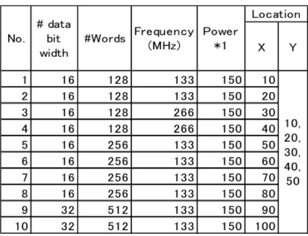
Table 1 shows the information of each memory used in the experiment. The 2-4th columns denote the data bit width, the word depth, the operating frequencies, respectively. The 5th column shows the power consumption. In this experiment, the power consumption of each memory is a relative value in which memory No.1 is assumed to be 100 under the following assumption.
a) The area is proportional to (number of words
×
number of bits).b) The power consumption is proportional to the area.
c) The power consumption is proportional to the frequency.
The 6th and 7th column shows location. In this experiment, the number of memories were changed between 3 and 50, and the program was executed respectively. In case, the number of memories N<11, we use No.1 to N, and for the rest, we extend the same set of No.1-10, with the Y coordinate changing 20 to 50.
In actual test, several background patterns (e.g. marching, checker, checker-bar) are used. But in this experiment, the test application time is calculated by assuming the number of background patterns=1. In addition, the following constraint values were used.
Maximum distance of memory connection: D=40 Maximum available peak power of the SoC:
P=5000
Maximum test application time of memory: T=300µs
Table1. Information On memories
, , , ,
#
#
Experiments are carried out for the following five cases: (1) Not shared (All the memories have individual BIST wrapper.), (2) Parallel connection (Memory BIST logic is shared by using only the parallel connection as described in the proposed technique.), (3) Serial connection (Memory BIST logic is shared by using only the serial connection as described in the proposed technique.), (4) Parallel and Serial connection (Memory BIST logic is shared by using the parallel connection and serial connection as described in the proposed technique.), (5) Exhaustive search (Memory BIST logic is shared by using only the parallel connection by exhaustive search.). Table 2 shows the experimental results. The 1st column shows the number of memories. The 2nd column shows the total area of memory BIST wrapper without sharing. The 3-5th column shows the total area of memory BIST wrapper using proposed techniques. The 3rd column shows the results that used only parallel connection. The 4th column shows the results that used only serial connection. The 5th column shows the results that used parallel connection and serial connection. The 6th column shows the minimum solution that is obtained by exhaustive search.
We could complete exhaustive search only when the number of memories are smaller than 7. In these cases, the results of exhaustive search show that memory BIST logic sharing technique can reduce the area of BIST wrapper between 21.59 and 47.83% as the minimum solutions. The proposed technique has the case achieved only of 64.45% of the minimum solution, and has room for improving the quality of the solution. The average reduction ratio of Parallel connection, Serial connection, Parallel and serial connection are 21.08%, 37.25%, 40.55%, respectively.
In all cases, Parallel and serial connection achieved best solution. From this result, it is shown that selection from two types of connection
methods is able to reduce more areas than using single connection method.
Finally, Fig.5 shows the execution time of the implemented memory grouping program. All the cases can execute with in 10 seconds using proposed algorithm. The proposed technique can obtain the result in a very small CPU time so that it is practical.
5. Conclusions
The memory grouping problem was formulated and the algorithm to solves the problem is proposed. The experimental results show that the proposed method reduced up to 40.55% area of memory BIST wrapper.
It is shown that selection from two types of connection methods is able to reduce more areas than using single connection method.
Our future work includes the following issues. (1) Improvement of quality of solution
(2) Minimization of test application time
Acknowledgements
Authors would like to thank Prof. Michiko Inoue and Prof. Satoshi Ohtake and members of Computer Design and Test Lab. (Nara Institute of Science and Technology) for their valuable discussions.
References
[1] A.Benso, S.Di Carlo, G. Di Natale and P. Prinetto, “A Programmable BIST Architecture for Clusters of Multiple-Port SRAMs,” in Proc. International Test Conf., pp557-566, October 2000.
[2] H. Nagamochi and T. Ibaraki, “A linear-time algorithm for finding a sparse k-connected spanning subgraph of a k-connected graph,” Algorithmica, vol. 7, 1992, pp. 583--596. [3] H. Nagamochi and T. Ibaraki, “Computing the
edge-connectivity of multigraphs and capacitated graphs, “ SIAM J. Discrete Mathematics, vol. 5, 1992, pp. 54--66.
[4]Charles E. Stroud, A Designer’s Guide to Built-In Self-Test, Kluwer Academic Publishers, The Netherlands, 2002.
[5]V. Iyengar, K. Chakrabarty and E. J. Marinissen,
“On using rectangle packaging for SOC wrapper/TAM co-optimization,” in Proc. VLSI Test Symposium, pp. 253-258, May 2002.
[6]Y. Huang, N. Mukherjee, S. Reddy, C. Tsai, W. Cheng, O. Samman, P. Reuter, and Y. Zaidan,
“Optimal Core Wrapper Width Selection and SOC Test Scheduling Based On 3-Dimensional Bin Packing Algorithm,” in Proc. International Test Conf., pp. 74-82, October 2002.
Table2. Area of Memory-BIST Logic
&
#
&
&
Fig.5 CPU Time of Memory Grouping program