A DFT Method for RTL Data Paths Based on Partially Strong Testability
to Guarantee Complete Fault Efficiency
Hiroyuki Iwata , Tomokazu Yoneda , Satoshi Ohtake , Hideo Fujiwara
Graduate School of Information Science Nara Institute of Science and Technology
Kansai Science City 630-0192, Japan
Email:{hiroyu-i,yoneda,ohtake,fujiwara}@is.naist.jp
Abstract
This paper presents a non-scan design-for-testability (DFT) method that guarantees complete fault efficiency (FE) for register transfer level (RTL) data paths. We first define the partially strong testability as a characteristic of data paths. Then we propose a DFT method to make a data path partially strongly testable and a test generation method for partially strong testable data paths based on the time expansion model (TEM). The proposed DFT method can reduce hardware overhead drastically compared with the previous method based on strong testability. Moreover, the proposed DFT method can generate test patterns with complete FE in practical time and allow at-speed test. key words: design-for-testability, data paths, strong testa- bility, partially strong testability, complete fault efficiency
1. Introduction
With the progress of semiconductor technology, testing of VLSI becomes more difficult and the cost is increasing. Therefore, it is important to achieve high FE with low cost. For combinational circuits, test patterns with 100% FE can be obtained by an automatic test pattern generator (ATPG) [1]. For sequential circuits, the test generation can be modeled by an iterative combinational arrays [1] so that a combinational test generation method can be used. How- ever, test generation for sequential circuits is more complex than that for combinational circuits because of the num- ber of time frames needed for the justification and the error propagation. In the worst case, the number of time frames is the exponential function of the number of FFs. To ease the complexity of the test generation, DFT techniques have been proposed.
The most widely used DFT techniques for sequential circuits is the full scan approach [1, 2]. In the full scan approach, test generation algorithm for combinational cir- cuits can be applied. Therefore, this approach can achieve 100% FE. However, it requires large hardware overhead and can not allow at-speed test.
To avoid these disadvantages, non-scan DFT methods have been proposed [3, 4, 5]. A DFT method for RTL data paths based on strong testability [4] can achieve 100% FE and allows at-speed test. Moreover, compared with the full scan design, it achieves shorter test application time and lower hardware overhead. This method is based on hier- archical test generation [6] that consists of the following two steps. First, test patterns for each hardware element are generated. Then, a test plan (control vector sequences) for each hardware element is generated so that any test pat- tern can be propagated from primary inputs to its inputs and test responses can be propagated from its outputs to a pri- mary output. Strong testability can be satisfied by adding thru function to all operational modules and hold function to some registers. Thru function propagates the value of the input of the hardware element to the output of the hardware element without changing the value. Hold function holds the value of the register. However, we can propagate any test pattern to each hardware element even if thru function is not added to all operational modules. Moreover, it is not necessary to propagate any test pattern to each hardware el- ement. We can test each hardware element by applying all the values that appear in normal operation to the inputs of the hardware element.
In this paper, we introduce partially strong testability of a data path and a DFT method for making a data path par- tially strongly testable. Partially strong testability guaran- tees that for every signal line l, any value that appears at l in normal operation can be set to l while strong testa- bility guarantees that every value whether it appears in normal operation or not can be set to l. In the proposed DFT method, only part of the hardware elements are aug- mented with DFT elements in order to make a data path partially strongly testable. Therefore, the hardware over- head is drastically lower than that required strong testabil- ity. Moreover, we propose a test generation method for par- tially strongly testable data paths. In the proposed method, a time expansion model (TEM) [7] is extended for partially strongly testable data paths. The number of time frames
IEEE the 14th Asian Test Symposium (ATS'05), pp. 306-311, Dec. 2005.
needed for justification and error propagation is the sum of a sequential depth from a primary input to a primary out- put along a simple path and a sequential depth of a loop. Therefore, the method can achieve 100% FE in practical test generation time by using a combinational ATPG. Fur- thermore, the proposed method can achieve shorter test ap- plication time than the method based on strong testability and allow at-speed test.
2. Preliminary
2.1. Data PathsIn RTL description, a VLSI circuit generally consists of a controller and a data path. In this paper, a data path and a controller are separated and only a data path is the object of testing. A data path consists of hardware elements and signal lines. Hardware elements are primary input (PI), pri- mary output (PO), hold register (HR), load register (LR), multiplexer (MUX), operational module (CM) and obser- vational module (OM). Inputs of a hardware element are classified into data inputs and control inputs. Similarly, outputs of a hardware element are classified into data out- puts and status outputs. A data input is connected with a data output of the other hardware element by a signal line. A control input is fed the signal from a controller. A status outputs feed the signal to a controller. We assume that con- trol inputs are controllable and status outputs are observ- able. Moreover, we assume that all data inputs and outputs of hardware elements have the same bit width as a restric- tion for a data path.
Each hardware element has at most two data inputs, at most one control input, at most one status output, at most one data outputs. We classify CM into two types : CMA and CMB. CMA is a operational module that can be set any value to the data output by controlling the data inputs. CMB is a operational module except for CMA. MUXs, CMs and OMs are called combinational hardware elements.
2.2. Strong Testability
Definition 1 (Strong Testability [4]) A data path is strongly testable iff there exists a test plan for each hardware element m that makes it possible to apply any pattern to m and to observe any response of m.
If a data path DP is strongly testable, test patterns with 100% FE for m in DP generated by using a test generation algorithm for combinational circuits can be applied the test patterns from PIs to m and the responses can be observed from m to a PO.
Let m be a hardware element in a data path, let dmibe the number of time frames required for propagation of the test patterns along a simple path from a PI to m, let dmobe the number of time frames required for propagation of the responses along a simple path from m to a PO. In the DFT method based on strong testability, the length of a test plan for m is dmi+dmo+1.
3. Partially Strong Testability
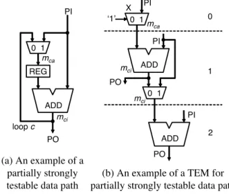
In this paper, we define partially strong testability to ap- ply combinational ATPG to a TEM of a data path and guar- antee that the number of time frames of the TEM is about the same as the length of a test plan of strong testability. An example of partially strongly testable data path and a TEM is shown in Figure 1.
Definition 2 (The Range of a Signal Line) Let Rlbe a set of values that can appear at a signal line l by controlling PIs. Then, Rlis called the range of line l. The range of the inputs/outputs of hardware elements connected with line l is defined as the range of line l.
Definition 3 (Dependency) Let Rliand Rl jbe the range of a signal line liand lj, respectively. There exists a depen- dency between li and lj if liand lj can not be simultane- ously set to any value in Rliand Rl j, respectively. A depen- dency of the inputs/outputs of hardware elements connected with li and lj is defined as the dependency between liand lj.
Definition 4 (Partially Strong Testability) Let L be a set of loops in a data path and let c be a loop in L. Let Mc
be a set of CMs with two data inputs and MUXs on c. A data path DP is partially strongly testable iff L satisfies the following conditions.
1. The data output of each hardware element mca∈ Mc
can be set to any value along a simple path.
2. Let mci be a hardware element in Mc Let dc be the number of time frames required for propagation of the values from mca to mci. There is no dependency be- tween a data output of maat time t and a data input on c of mciat time t + d.
Theorem 1 If DP is partially strongly testable, any de- tectable fault in DP are detectable in a TEM for partially strong testable data path and the number of time frames of the TEM is the maximum dmi+dmo+1 + nmCM. Let nmCM
be the number of CMs with two data inputs exist on a sim- ple path from a PI to a PO via m.
Proof: If DP is an acyclic structure, it is proved that any detectable fault in DP are detectable in a TEM by [8]. By condition 1 and 2 of partially strongly testability, any value in normal operation can be propagated to any hard- ware element on any loop by performing time expansion once along the loop. Moreover, any value in normal op- eration can be applied from PIs to any hardware element mby dmiframes and any value in normal operation can be propagated from m to a PO by dmoframes. Then, at most nmCMframes are needed so that there cannot exist a depen- dency between data inputs of CMs on a simple path via m. Therefore, if there are loops in DP and DP is partially strongly testable, any detectable fault in DP are detectable because a TEM of the DP can be treated as acyclic struc- ture. The number of time frames of a TEM is the maximum dmi+dmo+1 + nmCM.
ADD REG
0 1
PO PI
loop c mca
mci
(a) An example of a partially strongly testable data path
0 1 ADD 0 1 X
‘1’
PO PI
PI
0
1
2 ADD
PI
PO mca
mci
mci
(b) An example of a TEM for partially strongly testable data path Figure 1. Partially strong testability
4. DFT for Partially Strong Testability
4.1. Problem FormulationA given data path can be made partially strongly testable by adding thru function and hold function. We first formu- late a DFT problem for making a data path partially strong testable as the following optimization problem.
Definition 5 (DFT for Partially Strong Testability) input: a data path
output: a partially strongly testable data path and a TEM of a partially strongly testable data path
Optimization: minimizing hardware overhead
For CMs such as adders and multiplexers, we realize thru function by using a mask element instead of MUX be- cause the former requires lower area.
4.2. Overview of DFT Algorithm
This subsection describes the overview of the proposed heuristic DFT method. The DFT algorithm consists of the following three phases.
1. Construct a control forest: To satisfy the condition 1 of partially strong testability, we construct a set of simple paths which guarantee to propagate any value in the range of each signal line. The simple path is called a control path and a set of the paths is called a control forest. Thru function is added to CMs to prop- agate any value.
2. Resolve dependencies: To satisfy the condition 2 of partially strong testability, we find whether there ex- ists a dependency between data inputs of every hard- ware element. Hold function is added to LRs to re- solve a dependency.
3. Generate a time expansion model: For test generation, we generate a TEM. Hold function is added to LRs so that any detectable fault in a data path can be detected in only one TEM.
4.2.1. Control Forest Construction In the proposed method, in order to reduce the CMs to be added thru func- tion, if there are paths such that any value can be prop- agated along the paths without adding thru function, the paths are included in a control forest as much as possible. A control forest is constructed in order to decrease the de- pendencies of the control paths as much as possible and the ratio for the paths whose range is different from the range of a PI used as a control forest is the minimal.
We select the hardware elements and the paths from PI as the control forest. Let m be a hardware element, let mt
be a hardware element which is connected with a data out- put of m and not yet selected from m, and let nm be the number of mt. Let CC be a set of hardware elements such that the paths connected with all the data inputs of the hard- ware element are selected and there exists the path that is connected with a data output of the hardware element and is not yet selected. Let CM be a set of hardware elements with the minimum nm in CC. Let CREG be a set of regis- ters such that the path connected with a data inputs of the register is selected and all the path connected with a data output of the register are not yet selected. Let CCMbe a set of CMs such that at least one path connected with the data inputs of the CM is selected and all the path connected with a data output of the CM are not yet selected. The steps for constructing a control forest are shown as follows.
1. CC is initialized to a set of PIs. CREG,CCM are set to empty. All the hardware elements and the paths are not selected.
2. This step is repeatedly performed until CM is empty. CM is initialized to a set of hardware elements with the minimum nmin CC. We select m∈ CMand delete mfrom CM. Then, if there is no mt, m is deleted from CC. We select mt and the path between m and mt and operate as follows.
• If mt is a MUX and mt is selected in the first time, mtis added to CC.
• If mtis a HR or a LR, mt is added to CREG.
• If mtis a CMA, all the paths connected with data inputs of mt are selected and mt is never added to CC, mt is added to CC and deleted from CCM
iff mt exists in CCM.
• If mtis a CMA which does not satisfy above con- dition or mtis a CMB, mt is added to CCM. The selection from m is continuously performed until mtwhich is never selected is selected.
3. If CCis not empty, the process returns to step 2. 4. If CREGis not empty, all the registers in CREGis added
to CC and deleted from CREG and the process returns to step 2.
5. If there exists a CMA m∈ CCM, m is added to CCand deleted from CCM and the process returns to step 2. Then, if there exists no CMA in CCMand there exists
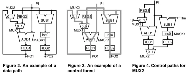
ADD1 REG3 0 1
REG1 PI
PO1
SUB1
REG2 ins0 MASK1
PO2 0 1
MUX1 MUX2
Figure 2. An example of a data path
ADD1 REG3
REG1 PI
PO1
SUB1
REG2 ins0 MASK1
PO2 MUX1
MUX2 0 1
0 1
Figure 3. An example of a control forest
0 1
SUB1
REG2 REG1
PI
MUX2
Thru
ins0 MASK1 ADD1
0 1 MUX1
REG3
‘1’
Figure 4. Control paths for MUX2
a CMB m∈ CCM, m is added to CC and deleted from CCMand it returns to step 2.
6. Let m be a hardware element, let in1mbe the data input of m connected with the path selected in the first time and let outm be a data output of m. If m satisfies at least one of following conditions, thru function that propagates from in1mto outmis added to m.
• There exists no register on the re-convergent path in a control forest which re-converge with m. And m exists on a loop or a loop exists on the path connected with the output of m.
• On the step 5, m is a CMA included in CCM.
• m is a CMB. And m exists on a loop or a loop exists on the path connected with the output of m.
An example of a control forest for Figure 2 is shown in Figure 3. In the example of Figure 2, after step 1-4, the hardware elements and paths except SUB1 or subsequent ones are selected. In step 6, thru function is added to SUB1. 4.2.2. Dependency Resolution It is assumed that there exists a dependency between two data inputs of a hardware elements if the control paths for the hardware element are a re-convergent path in a control forest which re-converge with the hardware element and the sequential depths of the re-convergence path are same.
Let mc be a hardware element such that there is a de- pendency between two data inputs of mc. If mc exists on a loop or there exist HRs on the control paths from mc to PIs, the dependency needs to be resolved. To resolve the dependency, the hold time of the registers adjacent to one data input of mcis figured out. If there exists the LRs in the registers, hold function is added to the LRs.
An example of control paths is shown in Figure 4. There exist control paths with the sequential depth 1 or 2 from the PI to the left data input of MUX2. There exists a control path with the sequential depth 1 from the PI to the right data input of MUX2. Therefore, there exists the dependency between the two data inputs of MUX2. The dependency
must be resolved because MUX2 exists on a loop. REG1 is holded one cycle so that the dependency can be resolved. 4.2.3. Time Expansion Model Generation A TEM is used for test generation of partially strongly testable data path. In the proposed method, a hold function is added of the process of a TEM generation so that only one TEM can be generated.
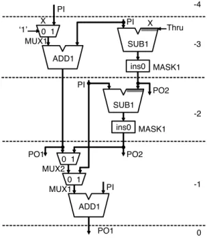
Let t be the current time frame number of a TEM. Let CO,CREG1.CREG2 be a set of hardware elements, respec- tively. The steps for a TEM generation are shown as fol- lows.
1. CO is initialized to a PO. CREG1,CREG2 are set to empty. t is set to zero.
2. This step is repeatedly performed until CO is empty. A hardware element md∈ COis deleted from COand md is added to the TEM at t. Then, we operate as follows. If mdis added to the TEM in the first time, hardware elements connected with all the data inputs of md are added to CO. If md is added to the TEM in the second time or more, hardware elements con- nected to mdon the control forest are added to CO. If md is a HR or a LR, md is added to CREG1. If there exists the dependency between the two data inputs of md, the registers are holded according to the already figured out in 4.2.2 so that the dependency can be re- solved. The signal lines between mdand the hardware elements added to CO are added to the TEM. More- over, if the signal lines connected with POs, the POs are added to the TEM.
3. If CREG1is not empty, the registers in CREG1which are loaded at t are added to CREG2. Let MDbe a set of CMs on the paths from the registers in CREG2to POs in the TEM. If there is the dependency between two data in- puts of m∈ MDand m exists on a loop, the dependency is resolved in order to guarantee observation of the values. The registers which are reached from a data input of m in the TEM are holded so that the depen- dency can been resolved and deleted from CREG2. If
0 -2 -3 -4
MUX1 ADD1 0 1
ins0 SUB1
ins0 SUB1
MASK1 MASK1 PI
-1
PO1 PO2
X Thru
0 1 ADD1 0 1 MUX1
PI PI
MUX2 X
‘1’
PO1 PI
PO2
Figure 5. An example of a TEM
there exists LRs in the register, hold function is added to the LRs. The hardware elements connected with the data inputs of the registers in CREG2are added to CO
and the signal lines between the registers and the hard- ware elements are added to the TEM. The registers in CREG2are deleted from CREG1and CREG2. Then, the t is decremented one and the process returns to step 2. 4. One of the POs and OMs which are not added to the
TEM is added to CO. Then, the process returns to step 2 as t is the adequate time not to appear combinational hardware elements redundantly as possible.
An example of a TEM for Figure 2 is shown in Figure 5. In Step 1, COis initialized to PO1. In Step 2, there exists the dependency between the two data inputs of MUX1 and MUX2. Then, REG1 is holded one cycle at−1. In Step 5, the operation from PO2 is not performed because PO2 appears at−1,−2.
The hardware elements with the data input connected with no hardware element in the TEM have thru function. The control inputs of the hardware elements are controlled according to the control forest and the data inputs are set to unspecified values. A combinational ATPG is applied to a generated TEM using the above-mentioned restrictions. The generated test patterns are transformed so that the test patterns can be applied to the original data path.
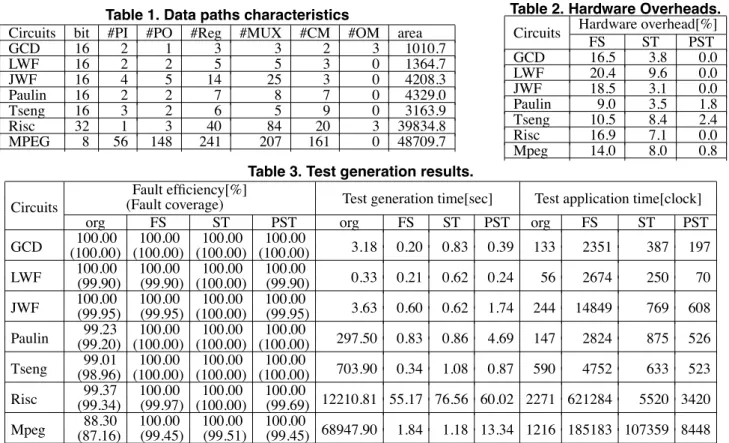
5. Experimental Results
We evaluate the effectiveness of the proposed method by experiments. RTL benchmark circuits used for the ex- periments are GCD, LWF, JWF and PAULIN, which are popularly used circuits [4, 5], and RISC and MPEG, which
are more practical and larger circuits designed by a semi- conductor company [4, 5]. Circuit characteristics of these circuits are shown in Table 1. Column “bit” denotes the bit width of the circuits. Column “#PI”, “#PO”, “#Reg”,
“#MUX”, “#CM” and “#OM” denote the numbers of pri- mary inputs, primary outputs, registers, multiplexeres, op- erational modules and observational modules, respectively. In our experiments, we used AutoLogicII (MentorGraph- ics) as a logic synthesis tool with its sample libraries to synthesize those circuits. In Table 1, column “Area” de- notes the total circuit size after synthesis.
We used TestGen (Synopsis) as a sequen- tial/combinational ATPG tool on Sun Blade 2000 (Sun Microsystems). Test generation for sequential circuits using a TEM requires a combinational ATPG which can deal with multiple stuck-at faults. In this experiments, since TestGen can not deal with multiple stuck-at fault, we use the circuit model which can express multiple stuck-at faults in a time expansion model as single stuck-at fault [9].
The results of the hardware overhead are shown in Ta- ble 2 and the results of test generation are shown in Table 3. Column “org”, “FS”, “ST” and “PST” denote results of the original circuits (without DFT), of the circuits modified by the full-scan design, of the circuits modified by the method of [4] and of the circuits modified by the proposed method, respectively. The value in parentheses in column “Fault efficiency” shows the fault coverage. Column “Test gener- ation time” denotes the time spent on the ATPG and does not include the time spent on the DFT since the time spent on the DFT is negligible as compared with the time spent on the ATPG. The test application time of the full scan de- signs are calculated by assuming the case where these cir- cuits have single scan chain.
The proposed method can always achieve drastically lower hardware overhead than both “FS” and “ST” can. Es- pecially for GCD, LWF, JWF and RISC, there is no need for DFT since the original circuits satisfies the partially strong testability as they are.
We observe that the test generation time of FS, ST and PST which can achieve 100% FE are much shorter than that of org. Moreover, PST can achieve almost same test gener- ation time as ST which is based on hierarchical test gener- ation. We consider that faults were efficiently detected by the fault simulation in PST since the whole circuit is the target for test generation in PST. However, PST requires a little bit long test generation time compared to FS. This is because PST uses a TEM for test generation.
In the result of test application time, PST can achieve shorter test application time than ST because faults were ef- ficiently detected by the fault simulation in PST. Moreover, PST can achieve much shorter test application time than FS. This is because PST does not require scan-shift oper-
Table 1. Data paths characteristics
Circuits bit #PI #PO #Reg #MUX #CM #OM area
GCD 16 2 1 3 3 2 3 1010.7
LWF 16 2 2 5 5 3 0 1364.7
JWF 16 4 5 14 25 3 0 4208.3
Paulin 16 2 2 7 8 7 0 4329.0
Tseng 16 3 2 6 5 9 0 3163.9
Risc 32 1 3 40 84 20 3 39834.8
MPEG 8 56 148 241 207 161 0 48709.7
Table 2. Hardware Overheads. Circuits Hardware overhead[%]
FS ST PST
GCD 16.5 3.8 0.0
LWF 20.4 9.6 0.0
JWF 18.5 3.1 0.0
Paulin 9.0 3.5 1.8
Tseng 10.5 8.4 2.4
Risc 16.9 7.1 0.0
Mpeg 14.0 8.0 0.8
Table 3. Test generation results. Circuits
Fault efficiency[%]
Test generation time[sec] Test application time[clock] (Fault coverage)
org FS ST PST org FS ST PST org FS ST PST
GCD (100.00) (100.00) (100.00) (100.00)100.00 100.00 100.00 100.00 3.18 0.20 0.83 0.39 133 2351 387 197
LWF 100.00(99.90) 100.00(99.90) (100.00)100.00 100.00(99.90) 0.33 0.21 0.62 0.24 56 2674 250 70 JWF 100.00(99.95) 100.00(99.95) (100.00)100.00 100.00(99.95) 3.63 0.60 0.62 1.74 244 14849 769 608
Paulin (99.20) (100.00) (100.00) (100.00)99.23 100.00 100.00 100.00 297.50 0.83 0.86 4.69 147 2824 875 526 Tseng (98.96) (100.00) (100.00) (100.00)99.01 100.00 100.00 100.00 703.90 0.34 1.08 0.87 590 4752 633 523
Risc (99.34)99.37 100.00(99.97) (100.00)100.00 100.00(99.69) 12210.81 55.17 76.56 60.02 2271 621284 5520 3420 Mpeg (87.16)88.30 100.00(99.45) 100.00(99.51) 100.00(99.45) 68947.90 1.84 1.18 13.34 1216 185183 107359 8448
ations. Furthermore, FS cannot allow at-speed test while other approaches can.
6. Conclusion
In this paper, we defined partially strong testability as a characteristic of a data path. We also proposed a DFT method for RTL data paths based on partially strong testability. The proposed method achieves 100% FE within practical test generation time by using combina- tional ATPG. It also allows at-speed testing. Furthermore, the hardware overhead required by the proposed method is drastically lower and the test application time is shorter compared with the method for strong testability [4].
Acknowledgments
The authors would like to thank Prof. Michiko Inoue of Nara Institute of Science and Technology for her valu- able discussions. This work was supported in part by 21st Century COE Program and in part by Japan Society for the Promotion of Science (JSPS) under Grants-in-Aid for Sci- entific Research B(2)(No. 15300018).
References
[1] H. Fujiwara, Logic Testing and Design for Testability, The MIT press, 1985.
[2] M. Abramovici, M. A. Breuer and A.D.Friedman, Digi- tal Systems Testing and Testable Design, Computer Science Press, 1990.
[3] R. B. Norwood and E. J. McCluskey, “Orthogonal scan:Low overhead scan for data Paths,” Proc.1996 Int.Test Conf.,pp.659-668(1996)
[4] H. Wada, T. Masuzawa, K. K. Saluja and H. Fujiwara, “De- sign for strong testabillity of RTL data paths to provide com- plete fault efficiency,” Proc. of 13th International Conf.on VLSI Design, pp.300-305, Jan. 2000.
[5] S. Ohtake, S. Nagai, H. Wada and H. Fujiwara,“A DFT method for RTL circuits to achieve complete fault effi- ciency based on fixed-control testabillity,” Proc. of ASP- DAC, pp.331-334, 2001.
[6] J. Lee and J.H. Patel, “Hierarchical test generation under architectural level functional constraints,” IEEE Trans. on Computer-Aided Design of Integrated Circuits and Systems, vol. 15, no. 9, pp. 1144-1151, Sept. 1996.
[7] T. Inoue, T. Hosokawa, T. Mihara, and H. Fujiwara, “An op- timal time expansion model based on combinational ATPG for RT level ciruits,” Proc. IEEE the 7th Asian Test Symp., pp. 190-197, Dec. 1998.
[8] T. Inoue, D. K. Das, T. Mihara, C. Sano and H. Fujiwara,
“Test generation for acyclic sequential circuits with hold registers,” International Conference on Computer Aided De- sign, pp.550-556, Nov. 2000.
[9] H. Ichihara, and T. Inoue, “A method of test generation for acyclic sequential circuits using single stuck-at fault combi- national ATPG,” IEICE Trans. Fundamentals, Vol. E86-A, No. 12, pp. 3072-3078, Dec. 2003.