Instruction-Based Self-Testing of Delay Faults
in Pipelined Processors
Virendra Singh, Member, IEEE, Michiko Inoue, Member, IEEE, Kewal K. Saluja, Fellow, IEEE, and Hideo Fujiwara, Fellow, IEEE
Abstract—Aggressive processor design methodology using high- speed clock and deep submicrometer technology is necessitating the use of at-speed delay fault testing. Although nearly all modern processors use pipelined architecture, no method has been pro- posed in literature to model these for the purpose of test gener- ation. This paper proposes a graph theoretic model of pipelined processors and develops a systematic approach to path delay fault testing of such processor cores using the processor instruction set. The proposed methodology generates test vectors under the ex- tracted architectural constraints. These test vectors can be applied in functional mode of operation, hence, self-test becomes possible. Self-test in a functional mode can also be used for online periodic testing. Our approach uses a graph model for architectural con- straint extraction and path classification. Test vectors are gener- ated using constrained automatic test pattern generation (ATPG) under the extracted constraints. Finally, a test program consisting of an instruction sequence is generated for the application of gen- erated test vectors. We applied our method to two example pro- cessors, namely a 16-bit 5-stage VPRO pipelined processor and a 32-bit pipelined DLX processor, to demonstrate the effectiveness of our methodology.
Index Terms—At-speed test, delay fault test, instruction-based self-test, microprocessor test.
I. INTRODUCTION
M
ODERN computer systems and systems-on-a-chip (SOCs) are built around very high-speed processors, in order to meet the increasing consumer demand of high performance and rich functionality with quick turn around time. Normally, these processor cores are preoptimized and implemented with deep submicrometer technology. Design reuse is being regarded as the only way that allows designers to keep pace with the technological developments. It reduces time to market and design effort. However, it introduces test diffi- culties. It is no longer sufficient to target conventional stuck-at faults; instead delay faults and crosstalk faults are becomingManuscript received September 20, 2005; revised April 5, 2006. This work was supported in part by Semiconductor Technology Academic Research Center (STARC) under the Research Project and by Japan Society for the Promotion of Science (JSPS) under Grants-in-Aid for Scientific Research B (2) under Grant 15300018, and by the JSPS Research Fellowship under Grant L04509.
V. Singh is with the IC Design Group, Central Electronics Engineering Research Institute, Pilani 333 031, India (e-mail: [email protected]; [email protected]; [email protected]).
M. Inoue and H. Fujiwara are with the Nara Institute of Science and Tech- nology, Nara 630-0192, Japan.
K. K. Saluja is with the Department of Electrical and Computer Engineering, University of Wisconsin-Madison, Madison, WI 53706 USA.
Digital Object Identifier 10.1109/TVLSI.2006.886412
increasingly important to keep pace with the rapid increase in the speed of integrated circuits. At-speed testing using an external tester is almost infeasible because of its inherent inaccuracy and cost. The widely used self-testing technique, built-in self-test (BIST), is a structural testing methodology that provides a good quality test. However, due to the need of design change, possibility of excessive power consump- tion that may result into burn out of chips, and unacceptable performance loss and area overhead, it is also not a feasible solution for high-performance processor cores. Further, it may be unacceptable to use hardware BIST for testing an optimized high-performance, low-power core embedded deep inside an SoC due to its poor and limited accessibility and its inability to accommodate design changes.
A practical research direction is instruction-based self-test (also known as software-based self-test) as an effective alter- native to hardware-based self-test. It links instruction-level test with the low-level fault model. Instruction-based self-test can be applied in the functional mode of operation. In order to apply test instructions in functional mode, it uses processor instruc- tions to deliver test patterns and collect the test responses. Thus, being inherently nonintrusive, it does not lead to area or perfor- mance overheads, or excessive power consumption. Therefore, it is the most suitable choice for testing optimized processor cores embedded deep inside an SoC. Moreover, the same test can also be used for the periodic online testing that contributes to system reliability, as it can be applied to a system in normal mode without affecting the system functionality.
This paper focuses on instruction-based self-testing method- ology. Nearly all modern processors use pipelined design, which motivated us to target pipelined processors. To the best of our knowledge, this paper is the first attempt towards the delay fault testing of pipelined processors in functional mode of operation using its instruction set. We use the path delay fault model, as this model is best suited for detecting real failures in high-speed circuits. A graph theoretic model is developed to model the behavior of a pipelined processor, and it is used for the test vector generation and test instruction sequence generation under the architectural constraints.
This paper is organized as follows. Section II describes the previous work done in the domain of instruction-based self- test. Section III describes the overview of our methodology and Section IV presents the graph model. Sections V and VI de- scribe the test generation process for datapath and controller parts of a processor. Section VII describes the instruction se- quence generation process. Section VIII presents experimental results to demonstrate the effectiveness of our methodology, and this paper finally concludes with Section IX.
1063-8210/$20.00 © 2006 IEEE
II. PREVIOUSWORK
A number of software based self-test approaches [2]–[7], tar- geting stuck-at faults, have been proposed for nonpipelined pro- cessors. The approaches proposed by Shen and Abraham [2] and Batcher and Papachristou [3] are based on instruction ran- domization, and are more functional in nature. Both these ap- proaches [2], [3] give low fault coverage due to high level of abstraction and they generate large code sequences resulting in large test application time. Chen and Dey [4] used the concept of self-test signature in which they generate structural tests in the form of self-test signatures for functional modules by taking constraints into consideration. These self-test signatures are ex- panded into test sets using software LFSR during self-test and applied using a test application program. Due to the pseudo- random nature of this methodology, the self-test code size and test application time are large. Moreover, efficiency of pseudo- random software-based methodology depends on internal archi- tecture and bit width. Kranitis et al. [5], [6] proposed a method- ology based on instruction set architecture and register transfer level (RTL) description while using deterministic test sets (uni- versal test set) to test every functional component of the pro- cessor for all the operations performed by that component. The deterministic nature of the approach reduced test code size but these methods find it difficult to achieve high fault coverage for complex architectures. Kambe et al. [7] presented a tem- plate-based approach for nonpipelined processors. A method- ology for a pipelined processor based on the test templates was presented by Chen et al. [8], which uses statistical regression for function mapping. Although it is a semi-automatic approach, it leads to long program size to achieve reasonable fault coverage for complex architectures due to its statistical nature. Kranitis et al.[9] also proposed a methodology for pipelined processors based on RTL description and instruction set architecture using deterministic tests for functional blocks, whereas Paschalis et al. [10] proposed an online periodic test methodology for pipeline processors. But these approaches [9], [10] target only functional blocks; hence, they are unable to achieve high fault coverage for complex architectures. Although [8]–[10] considered pipelined processor, the pipelined behavior was not considered explicitly in these, as they are largely focused on the functional blocks. Also none of the previously stated, approach target faults in a controller explicitly. Shamshiri et al. [20] proposed an approach for online self-testing that includes test instructions to run BIST during the idle time. As it uses hardware BIST, its hardware overhead is large for complex processors.
A few instruction-based self-test approaches targeting delay faults for a nonpipelined processor have also been proposed. The approach proposed by Lai et al. [11]–[13] first classifies a path to be functionally testable or untestable. The authors argue that delay defects on the functionally untestable paths will not cause any chip failure. This approach extracts constraints by exhaustively searching all possible instructions and instruction pairs which are applicable in the functional mode. The results for the controller are not presented. This approach assumes that a processor can be clearly divided into a datapath and a con- troller which does not hold good for pipelined processors. The
scope of this approach is limited to simple processors. An effi- cient graph theoretical model-based approach was proposed by us in [14] and [15]. This approach efficiently extracts the con- straints by using the graph theoretic model (called IE-graph) for the datapath and the state transition graph model for the con- troller and generates test vectors for the datapath and the con- troller. Constrained combinational automatic test pattern gener- ation (ATPG) is used for the test vector generation. These test vectors can easily be applied by using instruction sequences as these are generated under constraints. This approach is also lim- ited to nonpipelined processors, though it can handle architec- tural registers and finite state machine (FSM)-based controller. To the best of our knowledge, no approach has been pro- posed in literature for the testing of pipelined processors tar- geting delay faults so far. The consideration of pipeline behavior helps test generation process to a large extent for delay faults as it needs to consider the applicability of two-pattern tests in two consecutive cycles in the functional mode. Moreover, a system- atic and scalable approach can be developed by modeling the behavior of a processor. This is the motivating factor behind the present work. We believe this is the first work towards the mod- eling of pipeline behavior for testing of a microprocessor in the functional mode.
III. OVERVIEW OF THEAPPROACH
The objective of this work is to develop a procedure for delay fault testing of a pipeline processor/processor core that can be used to generate tests for the functional mode of operation of a processor using its instruction set. The main contributions of this work are as follows:
• develop a graph theoretic model for pipeline behavior using the RT level description of the processor;
• provide a systematic approach to test the processor based on the developed model;
• evaluate the method using experimental studies.
This paper presents a unified approach to test all normal and bypassing/forwarding paths in the datapath and all paths in the controller by using a graph model of the behavior of the pro- cessor. A hierarchical approach is presented for the test genera- tion which classifies paths and extracts the constraints for poten- tially functionally testable paths at RTL to generate test vectors at gate level using constrained ATPG. The path delay [16] fault model is used in this work.
Throughout this paper, the following concepts are used. Definition 1: A path [16] is defined as an ordered set of gates
, where is primary input or output from a flip-flop (FF), and is a primary output or input to a FF. Output
of a gate is an input to gate .
Definition 2: The number of pipeline stages bypassed by a path is defined as distance associated with the path.
Definition 3: A path is defined as functionally testable path if it is guaranteed to get a test vector to test in the functional mode. Definition 4: A path is defined as a functionally untestable pathif there exists no test vector (which can excite, propagate, and latch the result) to test in functional mode.
Definition 5: A path is defined as a parity check functionally untestable pathif it can be classified as functionally untestable on the existence of odd parity in the path.
Finally, we need one more definition to account for the aborted faults as well as for use during the test generation.
Definition 6: A path is defined as a potentially functionally testable pathif it is not classified as a functionally testable, func- tionally untestable, or parity check functionally untestable path. This definition is used to initially classify faults as potentially functionally testable and as we determine a fault to be either testable or untestable, it is moved from its class to the appro- priate class. This definition is most useful when parity check condition, described in Section V, is used to classify the paths.
Unlike a nonpipelined processor which completes execution of one instruction before the execution of the next instruction, in a pipelined processor multiple instructions can be in various stages of execution. These stages can be viewed as independent hardware units and all the stages execute instructions concur- rently. In order to support concurrent execution of instructions, necessary data and control signals are carried along as an in- struction progresses in the pipeline stages. Simultaneous exe- cution of multiple instructions can lead to data, control, and structural hazards. Data bypassing is a commonly used hard- ware technique to resolve data hazards; stalling is used for the unresolved hazards. Data flows from the first pipeline stage to the last pipeline stage during the normal execution (without any hazard). The simultaneous execution of multiple instruc- tions in various stages and the use of the data forwarding/by- passing mechanism make the behavior of the pipelined pro- cessor complex.
It is very difficult to separate datapath and controller parts clearly in a pipelined processor as every pipeline stage carries all the data and control signals required by the pipeline stages ahead of it. Nonetheless, our model defines them clearly and considers the paths in the datapath part and the control part separately. The data transfer activities between the architectural registers and data and address (memory address and register address) part of the pipeline registers is assumed to be in the datapath. The paths, which go through the control logic, are considered in the control part. The activities in datapath are controlled by the control sig- nals which are carried forward with the data; thus, the function of datapath is constrained by the controller. Hence, only a subset of structurally applicable test vectors may be applied in the func- tional mode of operation due to the presence of constraints.
A graph theoretic model called pipeline instruction execution graph (PIE-graph), has been developed that is constructed by using the instruction set architecture and RTL description. It is based on the instruction execution graph (IE-graph) introduced by us in [14] and [15], and the ground breaking work of Thatte and Abraham [1], for nonpipelined processors. This graph models the complex pipeline behavior. Our present model classifies paths as functionally testable (FT), functionally untestable (FUT), potentially functionally testable (PFT), and parity check functionally untestable (PCFUT) paths. After the classification, it extracts constraints for the PFT and PCFUT paths. First, constraints on the control signals in one or more relevant pipeline stages are extracted and then the constraints on justifiable data in the data registers or pipeline registers
Fig. 1. Test program flow.
under the control constraints are extracted. PCFUT paths are further classified as FUT paths or PFT paths. A combinational constrained ATPG is used for the test vector generation for the PFT paths. We can get test sequences without using ATPG for FT paths, and no test sequence is needed for FUT paths. For testing the controller, the constraints on the legitimate values for a group of control signals are extracted by using the RTL description. PIE-graph is used along with these constraints for further extraction of control and data constraints for target paths through controller, and their classification. Constrained ATPG is used to generate the test vectors. Finally, instruction sequences to apply the test vectors, are generated by using the knowledge of the control signals of various pipeline stages and the PIE-graph. Test program generation flow is shown in Fig. 1.
IV. PIPELINEINSTRUCTIONEXECUTIONGRAPH
Data transfer activities between the data registers of a pipelined processor can be modeled by the PIE-graph, which as stated earlier, is based on the IE-graph, introduced by us in [14] and [15], for nonpipelined processors. The IE-graph models the behavior of a simple nonpipelined, FSM-based processor. The PIE-graph can be constructed from the instruction set architecture and RTL description of a processor. It captures the pipeline behavior. This includes architecture registers and data and addresses part of the pipeline registers. Note that this does not include the control part of the pipeline registers.
We noticed that many paths directly transfer data to the next stage using simple interconnects or through a set of multiplexers. Keeping this in mind we classified logic into three types: 1) interconnect ; 2) multiplexers ; and 3) processing logic . This classification simplifies the test generation process. This information can be obtained from RTL description even when the full structural description is not available.
Nodes of the PIE-graph are as follows: 1) architectural registers;
2) part of architectural registers which can be independently readable and writable;
3) equivalent registers (set of registers which behave identi- cally as a group with instruction set, such as register file);
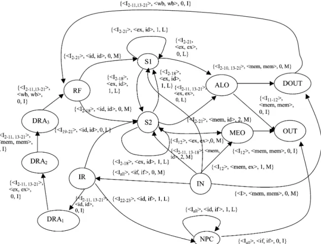
Fig. 2. PIE-graph of VPRO processor.
4) two special nodes, IN and OUT, which model the external world such as memory and input/output (I/O) devices; 5) data and address (memory address and register address)
part of pipeline registers.
If an architectural register is independently readable and writable in parts, then the architectural register is represented by the number of nodes equal to the number of independent parts (category 2) rather than a single node (category 1).
A directed edge between two nodes is drawn iff there exists at least one instruction responsible to transfer data (with or without manipulation) over the edge (paths) between the two registers corresponding to nodes. Each edge is marked with a 4-tuple
. This 4-tuple signifies that a set of instructions is responsible for the data transfer from stage to stage through the logic type , and the pair of instructions for delay testing must be separated by the cycles specified by the .
If a pipeline register is a source node, then the pipeline stage succeeding it will be stage; otherwise, the stage controlling the data transfer activities in the register will be in . If a pipeline register is a destination node, then the stage just before it (whose data it is latching) will be
stage, otherwise the stage that controls the data write activity in the register is . Data transfer activities inside a pipeline stage are modeled by keeping the same
and and zero distance, and the data transfer activities
across the pipeline stages (mainly bypassing paths) are mod-
eled by using , and appropriate distance
to create hazard in order to transfer data over that.
We will use a 16-bit, 5-stage pipelined processor VPRO de- sign with commonly used 24 instructions to demonstrate the concept. This processor uses load/store RISC architecture. It has register type, immediate type, and jump type instruction for- mats. This contains nearly all features of the pipelined RISC processors. A complete PIE-graph of VPRO is shown in Fig. 2, and the processor description is given in the appendix and in [19].
The PIE-graph of the VPRO processor consists of 13 nodes and 26 edges, whereas the PIE-graph of the pipelined DLX pro- cessor consists of 24 nodes and 48 edges. The complexity of the PIE-graph does not grow linearly with the processor complexity, e.g., with increase in bit width, number of general purpose reg- isters, or instructions, etc. In fact, increase in the bit-width and the number of registers in a register file do not affect the com- plexity of the graph. Hence, we believe that it is manageable for a modern pipelined processor and it should be addressable by tools once it is developed. The PIE-graph generation process is still manual. It is not automated because of different styles of writing the RTL code.
V. DATAPATH
This section deals with the paths that transfer data between architectural registers or data and address part of the pipeline
registers, which are significant in number. Other paths will be considered in the control part. The key idea behind this work is to develop a hierarchical and systematic approach which can achieve very high fault efficiency. In order to achieve this, the datapathof a pipeline processor is modeled by a PIE-graph. The developed graph model, along with the high level information (ISA and RTL description), is used to classify the paths at high level. This classification leads to eliminating those paths which cannot be excited in the functional mode. This section, based on the graph model, analyzes the conditions under which a fault can be excited in the functional mode and extracts the exact constraints. Moreover, it also facilitates the instruction sequence generation process.
We assume that any instruction can be followed by any other instruction in a pipeline stage except those instructions, which always need stall after the execution such as unconditional jumps. In order to test a path from register to register , we must create a transition at and capture the transferred data at . Although there may be paths with (bypass paths) to , there is guaranteed to be a path with zero distance (normal path) which brings the same values as the bypass paths, and hence, we only need to consider the normal path
for data transfer to . We also allow the propagation of data to through normal paths except from . This observation prunes the search space substantially.
Definition 7: Instructions, which behave identically within a pipeline stage, are defined as equivalent instructions, for that stage.
For example, ADD and INC behave identically in the EX stage of the VPRO processor; hence, these are the equivalent instructions in the EX stage. Similarly, instructions (ADD, ADDU, ADDI, ADDUI, LW, LH, LB, SW, SH, SB) are the equivalent instructions for the EX stage of the pipelined DLX processor. We can use these equivalent instructions to reduce the marked instructions which, in turn, reduce the constraint extraction and test generation effort. We make a table of the equivalent instructions for every stage, which is also used during instruction sequence generation.
Example 1: The bypass paths from memory to register S1 of the VPRO processor (represented by an edge between IN and S1) can be tested by the following instruction sequence:
The edge between IN and S1 is marked with distance 2, which means these paths bypass two pipeline stages. We need four in- structions to test these paths. The instructions and launch a transition from memory and propagate the launched transition in the mem stage, and the instructions and propagate the tran- sition in the decode stage. Finally, the instruction transfers the result to register R4. During the first cycle, the instructions and execute concurrently in the mem stage and decode stage, respectively, and during the second cycle, the instructions and
Fig. 3. Target path and pipeline stages.
execute concurrently in the mem stage and the decode stage, respectively. Therefore, this sequence can test the paths from IN to S1.
A path from register to register , marked with LT , where LT I,M,L , can be tested by a test instruction sequence IP IP ID ID IS IS , where ID ID ID are the filler instructions. To test a path, we need constraints for both stages and in two consecutive cycles (as shown in Fig. 3). Instruction pair (IP , IP ) is responsible to create a transition at register and allows it to propagate in the stage. The instruction pair (IS , IS ) is responsible to propagate the created transition in the stage and, finally, instruction IS latches the result in register
. The instructions IP and IS must be executed concurrently in the stages and , respectively. Similarly, the instructions IP and IS must be executed concurrently in the stages and , respectively. Other instructions ID ID are used to provide the proper distance between the instructions IP and IS , so that a transition along the path can be excited, propagated, and the result will be latched. We assume that data from other stages (for example, data from in Fig. 3) come through MUX and such data do not affect the data transfer along the target path. Therefore, ATPG does not care for these values and we do not need to extract their constraints. For example, in example 1 the data transfer from the mem stage to the ID stage selects the appropriate MUX control signal. This selection automatically deselects the other data transfer from the EX stage or the ID stage. Therefore, ATPG need not consider dataflow from the other stages. A sequence of instructions is needed to test these paths. Note that IP IS if
, and IP IS and IP IS if .
Instruction pair (IP and IP ) must be marked on any zero distance (with ) in-edge of and instruction pair (IS and IS ) must be marked on the target path (edge between and ). If source node is IN node then any load instruction can be used as IP or IP . If the target path is inside a pipeline stage then we don’t need dummy instructions, and are left with an instruction pair (IS and IS ). The instructions IS and IS must be marked on any zero distance in-edge of and at target edge, respectively.
A. Path Classification and Constraint Extraction
Our approach classifies all paths into four categories, which are: 1) FT paths; 2) FUT paths; 3) PFT paths; and 4) PCFUT paths. We can get a test sequence without using ATPG for FT paths, whereas we do not need to generate test for FUT paths. For the rest of the categories we need to extract architectural constraints.
There are two types of constraints: control constraints and data constraints. Control constraints are the constraints on con- trol signals, which are responsible for transfering data between two nodes. These are obtained from the PIE-graph. Data con- straints are the constraints on justifiable data under the control constraints. Control constraints are extracted as instruction pairs (IP , IP ) and (IS , IS ). Note that the nonrobust test [16] does not take care of first vector for off inputs. Therefore, we need to extract a set of instructions for IP and IS instead of instruc- tion pairs (IP , IP ) and (IS , IS ). We can easily get the set of instructions for IP and IS from the instructions marked on the input edge to and on the target edge, respectively.
Let there be an edge between nodes and , marked with LT . Constraints for paths of various types of logic are extracted as follows:
1) when the logic type is interconnect “ :”
These paths are generally used to carry forward data to the next stage and are always with . has only one in-edge, which is from . An instruction sequence (IS , IS ) is needed to test. Any instruction marked on the zero distance in-edge of register , can be used as IS , and any instruction marked in the target edge can be used as IS . These two instructions give the constraint on the control signals in the stage. has no other in-edge; hence, it will not observe any data constraint. These paths can be tested as interconnects test. Therefore, these paths are classified as FT paths;
2) when logic type is multiplexer “ :”
These paths pass through a set of MUXs and behave as in- terconnects if control signals are properly assigned. There- fore, under the control constraints (proper assignment of MUX select signals), data constraints are not applicable, as other paths to will automatically be deselected with the proper assignment of MUXs control signals. These paths can be tested as interconnect test;
We consider two different distance cases separately: a) when (normal flow inside a pipeline stage):
These paths transfer the data inside the same stage. Therefore an instruction pair (IS , IS ) is needed to test these paths. Any instruction marked on the zero distance in-edge of can be used as IS , and any instruction marked on the target edge can be used as IS . Instruction pair (IS , IS ) gives the constraints on the control signals in the stage. These paths always find a sequence of instructions without any data constraints, hence, classified as FT paths; b) when (data flow across the pipeline stages, i.e.,
forwarding path):
These paths are responsible for the data transfer across the pipeline stages. These paths are classified as FUT paths if these are marked with and have a self-loop because a transition cannot be launched. Other paths can be tested by an instruction sequence IP IP ID ID IS IS . The instructions IP and IP must be marked on any of zero distance in-edge of , and the instructions IS and IS must be marked on the target edge. Therefore, the instruc- tion pair (IP , IP ) gives the control constraints on
Fig. 4. Edge consideration for constraint extraction: (a) structural organiza- tion and (b) edges in PIE-graph.
the control signals of stage , and the instruction pair (IS , IS ) gives the constraints on the control signals in stage . These paths are classified as FT paths; 3) when logic type is processing logic “ :”
This includes the paths which pass through the combina- tional logic. Let an edge between two registers and
be marked with LT . The following
edges and nodes must be considered: 1) all the in-edges to with distance and logic type “ ” (having some in- structions common with ); 2) all the in-edges to with zero distance, logic type “ ,” and have some instruc- tions common with ; and 3) all zero distance
in-edges to .
All those registers which have out-edge to (with dis- tance —same as distance of target path, logic type “ ,” and some instructions common with the target edge) pro- vide the data constraints for the propagation of created transition in the stage. All those registers which have out-edge to (with zero distance, logic type “ ,” and have some instructions common with the target path) pro- vide data constraints for the propagation of the created transition in the stage. Fig. 4 shows the edges and nodes which are needed to be considered. Note that
, and ;
We consider two different distance cases separately: a) when (Normal flow inside a pipeline stage):
This includes the paths in a single stage. We need an instruction pair (IS , IS ) for testing. IS can be any instruction among the instructions marked on the in-edge of , and IS can be any instruction among the instructions marked on the target edge. An instruc- tion pair (IS , IS ) gives the constraint on the control signal in the stage. We have to find out the data con- straints on all those registers which have zero distance in-edge to with logic type “ ” using the PIE-graph and RTL description. Let have an in-edge from register which is marked with common instruc- tions with the target edge. Data constraints for these registers can be obtained as follows.
If the selected instruction IS is not marked on any of the in-edge of , then the register must have constant value across two time frames (under IS and IS );
b) when (data flow across pipeline stages, i.e., forwarding path):
These paths are responsible to transfer data across the pipeline stages. These paths need consec- utive instructions IP IP ID ID IS IS to test, which consists of filler instructions to excite these paths. IP and IP can be any instruction marked at any zero distance in-edge of , and IS and IS can be any instruction marked at target edge. Instruction pair (IP , IP ) gives the control constraints on the control signals of the stage, and instruction pair (IS , IS ) gives the constraint on the control sig- nals of the stage. Note that IP IS for , and we need an instruction sequence IP IS IS to test a path.
If an edge between register to is marked with logic type “ ” and , then the paths from bit to bit of register represents a self-loop. The paths between bit to bit of the register can be function- ally testable only when an odd inversion parity exists in the path, i.e., when the odd number of gates which can invert the logic (e.g., NOT, NOR, etc.) exists, oth- erwise, these paths are functionally untestable. These paths are classified as PCFUT. Many paths of this kind exist in the circuit, such as paths in the pass logic of ALU, paths in shifter, paths in logic operation block of ALU, etc. The rest of the paths are classified as PFT paths.
Instruction pair (IP , IP ) imposes constraints on those registers which have out-edge to with distance , logic type “ ” and some instructions common with the target edge. Instruction pair (IS , IS ) imposes data constraints to those registers which have zero distance out-edge of logic type “ ” to register with some instruction common with the target edge. Let register have out-edge to which is marked with distance , logic type “ ,” and have some common instructions with target edge, and a register have zero distance out-edge to which is marked with logic type “ ,” and has some common instructions with target edge. Register must have constant value across two time frames (under IP and IP ) if selected instruction IP is not marked on any in-edge of . Register must have constant value across two time frames (under IS and IS ) if selected IS is not marked on any the in-edge of .
Note that during stall cycle a path cannot be excited. The path can be excited when a stall cycle is followed by a nonstall cycle that can also be achieved in normal condition (without stall) and the previously stated pro- cedure can be used.
Example 2: Paths from the node S1 to ALO in the VPRO processor:
Paths from S1 to ALO are marked with
as shown in Fig. 5. This implies that any instruction from to can transfer data on the target path. We consider only normal data flow for the paths other than
Fig. 5. Edge consideration for the paths between S1 and ALO.
the target paths. Register S1 has only one zero distance edge
marked with the tuple . Therefore, IS
can be any instruction from to , and IS can also be any instruction from to . We can extract constraints in terms of instruction pairs and convert them into pairs of control signals (alu control and comparator control). Register S2 also has an
out-edge with ALO marked with ,
which provides the data constraints. Since the register S2 does not have any instruction marked at the in-edge which is not marked at the zero distance in-edge of S1, these paths do not observe data constraints. Since there are no constraints on data registers, we can find the values for control signals (ALU control signals and comparator signals) for the set of valid instructions for IS and IS , i.e., set of control signals for instructions to . All the possible combinations of control signals under IS and IS are the control constraints. Eight sets of control signals have been extracted under IS and the same eight sets for IS .
B. Test Vector Generation
An inversion parity test program, which checks the parity of the path, is used to further classify PCFUT paths into FUT paths or PFT paths. The previously stated procedure can be used to simplify the circuit for ATPG. Constrained ATPG is used to generate test vectors for all the PFT paths by using extracted constraints. ATPG is given with PFT paths and their respective extracted constraints, and it returns the test vectors if paths are functionally testable or identifies these to be untestable.
In order to generate test vectors under functional constraints, a PODEM-based delay fault test generation algorithm is im- plemented. For each PFT path, at first, it generates test vectors under extracted constraints for a nonrobust (NR) test if it exists. Otherwise, it declares the path as functionally NR untestable and generates the test vector under extracted constraints for that path for a functional sensitizable (FS) test if it exists. If a FS test does not exist then it identifies that path as a functionally FS untestable path. The algorithm flow is shown in Fig. 6.
VI. CONTROLLER
This section deals with the paths that contribute to control sig- nals. Any path, which goes through control logic, is dealt with in this section. In order to execute an instruction, the instruc- tion is decoded by the decode unit (in the decode stage). The decode unit dispatches control signals along with the required data to the pipeline stages ahead. Therefore, each pipeline stage has control signals that are not structured in nature but most of the time these can be grouped together in a small group.
Fig. 6. Constraint test generation flow.
A. Path Classification and Constraint Extraction
In our approach, a small grouping of control signals is used to find constraints. We need to extract two types of constraints: 1) constraints on the legitimate values of the group of control signals and 2) constraints on inter group signals in a pipeline stage.
1) Constraints on the Legitimacy of Signals: Control signals generally form a group of a small number of signals, where every possible value is not valid. Therefore, we need to ex- tract all the legitimate values. Test patterns must be generated under the legitimate values. For example, comparator control (comp_ctrl) signals in VPRO are grouped in a group of 3 bits, and the legitimate values are and .
2) Constraints on Inter Group Signals: It is not sufficient to consider only the legitimate values for a group of signals but we also need to consider the legitimacy of the inter group sig- nals in a pipeline stage, as all the possible combinations are not valid. We extract these in terms of instructions, i.e., map the con- trol signals to the instructions which can generate the particular combination and all possible combinations are extracted. For example, in VPRO when ALU ctrl (alu_ctrl) signal is the comparator control (comp_ctrl) signal must be .
The part of a pipeline register which carries the control sig- nals is called the control register (CR). There may be paths from the CR to the CR, the CR to the data register (DR), the DR (such as IR) to the CR, or the DR to the DR through control logic. Paths from CR-to-CR are used to carry the control signals for the pipeline stages ahead. These paths are usually connected directly and can always be tested as interconnect tests. Hence, these paths are classified as FT paths. Test vectors are generated under the previously stated constraints. Paths from the DR to
the CR are usually present in the decode stage. These paths are classified as PFT paths, and the test vectors for these paths can be generated under the previously stated constraints. Paths from CR to DR are the paths which pass through the combinational logic and are significant in number. We construct a table that shows the transition on some bit in CR with instructions after exclusion of equivalent instructions.
Let there be a path between a bit of control register and data register . Constraints can be extracted in the following manner:
1) when control register and data register are in the same stage:
It needs an instruction sequence of two instructions (IS , IS ). All those instruction pairs that can produce a transi- tion at bit and those are also marked on the in-edge of the register can be the test instructions (IS , IS ). All the data registers that have zero distance out-edge to (have some common instructions with the selected potential in- struction pairs) are needed to check for data constraints. Data constraints can be obtained in the same way as we ob- tain for datapath. These paths are classified as PFT paths; 2) when control register and data register are in dif-
ferent stages:
Register must have an edge from a register that lies in the same stage in which lies. This edge gives us the distance (say ), and we need a instruction se- quence IP IP ID ID IS IS to apply a test. All those instructions which can produce a transition at bit of and marked on any of the in-edge of those regis- ters which have out-edge to with same distance , can act as IP , and IP . Constraints on those registers which have out-edge to (with distance ) must be considered under IP , and IP . All those instructions which are marked on the in-edge of (with ) can act as IS and IS , and data constraints on those registers which have zero distance out-edge to must be considered under the control constraints of IS , IS instructions. These data con- straints can be obtained in the same way as in datapath. These paths are classified as PFT paths.
Paths from DR to DR through control logic, usually carry con- trol signals to multiplexers in the forwarding paths. Let there be a path from register to .
1) when both registers and are in the same stage: Register must have zero distance in-edges. The in- structions marked on these edges provides the control con- straints. These paths do not observe data constraints and these are classified as PFT paths.
Depending on the multiplexer control signals, an in-edge to is selected which forwards data during this test. Let that edge be marked with distance . These paths can be tested by an instruction sequence
IP IP ID ID IS IS ;
2) when both registers and are in different stages: Register must have an edge from a register that lies in the same stage in which lies. The edge from to gives us the distance (say ). The test vec- tors can be applied through an instruction sequence IP IP ID ID IS IS . All the instructions
marked on the edge from to can act as IS and IS . All the instructions marked on the in-edges of can act as IP and IP . These paths do not observe data constraints and these are classified as PFT paths.
B. Test Vector Generation
Constrained ATPG, as discussed in Section V-B, is used to generate test vectors for all the PFT paths under the extracted constraints. ATPG is given with PFT paths and their respective extracted constraints, and it returns the test vectors if the paths are functionally testable or it identifies these to be untestable.
VII. TESTINSTRUCTIONSEQUENCEGENERATION
The generated test vector pairs as explained before are as- signed to control signals and registers. A sequence of instruc- tions is needed to apply these test vectors. This process needs the following three steps:
1) test instruction sequence generation; 2) justification instruction sequence generation; 3) observation instruction sequence generation.
Test instruction sequence generation step generates a se- quence of instructions which is responsible to launch the transition, propagates the launched transition, and latches the result provided that desired data are available in the appropriate registers. These data are made available by the justification instruction sequence. Finally, the result must be transferred to memory by a sequence of instructions, called observation sequence.
1) Test Instruction Sequence Generation: We have generated the test vectors for the paths between a register pair, under ex- tracted constraints, and the information regarding the registers is available to us. We can use this information and PIE-graph to generate test instructions, which make this process simpler. It is clear from the earlier discussion that if an edge between regis-
ters and is marked LT , then we need
an instruction sequence IP IP ID ID IS IS to apply the test vectors provided that test vectors are available in desired registers. Instructions IP (when ) and IP (when ) are decided by the control signals of the stage , and instructions IS and IS are decided by the control signals of the stage. If there are more than one potential candidates for these instructions then we must select an easy to observe instruction (such as STORE) for IS and an easy to justify instruction for the rest. Once IP , IP , IS , and IS instructions are decided, we fill the rest of the instructions by NOP instructions which can be replaced later on by the justification instructions for IS and IS that can reduce the number of instructions.
2) Justification Instructions: During the test instruction se- quence generation, we assumed that the desired data are avail- able in appropriate registers. Now, we need to generate a se- quence of instructions to justify the data in the registers.
We cannot directly justify data in the pipeline registers. Therefore, we map back the data to either memory or architec- ture registers where we can justify easily. In order to do this, we construct a table that maps every pipeline data/address register to a justifiable register or memory and to an output register or
TABLE I
REGISTERMAPPING—VPRO PROCESSOR
TABLE II
RESULTS FORVPRO PROCESSOR
TABLE III
RESULTS FORPIPELINEDDLX PROCESSOR
memory when we execute some particular instruction. Such a table for VPRO is shown in part which contain some of the mapped I/O in Table I.
We use Table I to find the register/memory where we need to justify data. Simple justification instructions are used. A routine developed specifically for justification of a value in a special register, is used to justify the value in the special register. For example, we need to have a sequence of instructions, as opposed to a pair of instructions, to justify the data in the status register which sets some flag(s).
3) Observation Instructions: Result from the register must be transferred to memory. The instruction IS transfers data to some output register or memory, and that information we can get from Table I. If it is transferred to memory then we do not need any observation instruction, otherwise, we need to transfer data from register file to memory using the STORE in- struction. A special routine is used for the data transfer from the special registers and the control registers. For example, data from a status register can be observed by a sequence of instruc- tions which checks the status of different flags.
Example 3: Consider a test vector pair for a path between registers S1 and ALO of the VPRO processor
,
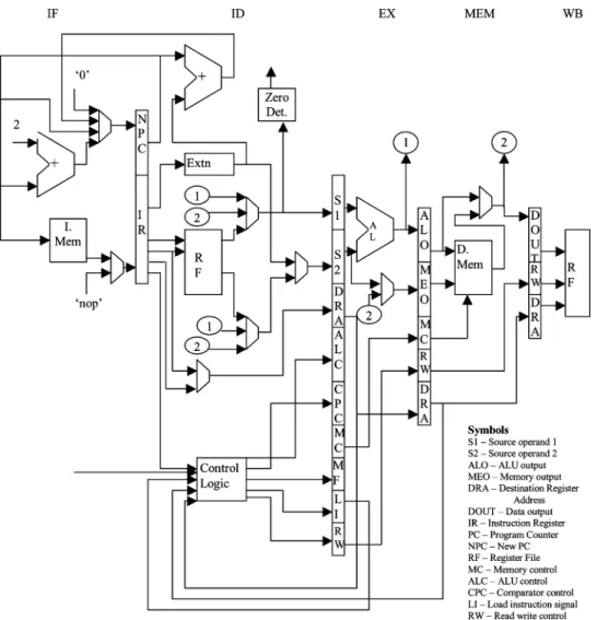
Fig. 7. Structural organization of VPRO processor.
and
. The test instruction sequence will be
where and
This edge is marked with . Therefore, we need two test instructions IS and IS which can be obtained from the control signals of the execution stage. Control signals imply that the instruction IS must be ADD (provide ,
) and IS must be SUB (provide
, ). We map pipeline register S1 and S2 to memory or architectural registers using a mapping table. Both these registers are mapped to the register file. We must choose four different registers from the register file to justify the value. Let R1 and R2 be chosen for S1, and R3 and R4 be chosen for S2. The content of R1, R2, R3, and R4 must be 0024H, 0004H, 0428H, and 0224H, respectively. We must also map the output pipeline register to memory or architectural register using the mapping table. ALO is mapped to the register file. Therefore, we must once again choose some register from the register file, and let it be R5 (it can also be R1 or any other register). Test
instructions will be ADD R5, R1, R3, and SUB R5, R2, R4. In order to observe the result we have to transfer data to memory. Observation instruction will be STORE instruction. In order to justify data in registers R1, R2, R3, and R4, we need LOAD instructions.
The previously stated method can generate a test sequence to apply the generated test vectors under architectural constraints. However, in theory, it is possible that a fault effect (error) that is captured in a register may be masked when the results are propagated for storage in the memory, or even the justifica- tion sequence may not be valid. It may happen due to mul- tiple excitation of the same fault either during the justification process or during the observation process. But, we believe that the likelihood of this to happen is very little and in any case such fault masking can be identified by fault simulation. If a fault is masked by the justification sequence then the fault effect from the justification sequence can be directly transferred to memory by an observation sequence without going through the test in- struction sequence, because the fault is already excited by the justification instruction sequence. If a fault is masked by the ob- servation sequence then it can be eliminated by the insertion of some dummy instruction(s) between the test instruction se- quence and the observation instruction sequence. Hence, fault masking can be eliminated.
VIII. EXPERIMENTALRESULTS
We have applied our methodology to two processors namely 16-bit 5-stage pipelined VPRO processor and 32-bit 5-stage pipelined DLX processor. The VPRO processor has been syn- thesized using 2345 gates and 268 sequential elements, and the pipelined DLX processor [17] is synthesized with 34 347 gates and 1898 sequential elements. Complete PIE-graphs for both processors are constructed by using instruction set architecture and RTL descriptions. The PIE-graph is used for the constraint extraction and the path classification. Our developed con- strained ATPG for path delay faults is used, as commercially available ATPG are not capable of handling constraints.
Results for the VPRO and DLX processors for the NR and FS [16] tests are shown in Tables II and III, respectively. The order of the generation of test vectors is the NR test followed by the FS test. For each path, at first, ATPG generates a test vector pair for the NR test, if it exists under the extracted archi- tectural constraints. Otherwise, it generates the test vector pair for the FS test if it exists under architectural constraints. The FS testable paths include the NR testable paths. The abort limit was set to 500. Here, we considered a path that goes through the control logic as a part of the controller. The results show that only a small fraction (about 24%) of paths are function- ally testable. However, we achieve 100% fault efficiency in the test generation. These test vectors are generated under architec- tural constraints; hence, these can be applied through instruction sequences. As pointed out in Section VII, these instruction se- quences may lead to fault masking due to the observation and the justification sequences. Fault masking can be identified by fault simulation and eliminated as explained in Section VII.
We now estimate the size of the test programs to test these processors. In order to apply a test vector pair, a sequence consisting of approximately 15 instructions is sufficient as follows. We need a sequence of about eight instructions to load operands, about four test instructions—without filler instruc- tions, one observation instruction, and about two instructions to load the memory locations. Therefore, a maximum of 2 858 130 instructions are needed to apply the generated 190 542 test vector pairs for DLX processor. Assuming each instruction to be 4 bytes, we need 10.9-MB storage space. Such a test program will take 37 ms to run on a 100-MHz implementation of a DLX processor, assuming on average 30% stalls during execution. Although these numbers can be reduced substan- tially by merging some vector pairs. None the less, these figures (storage requirement and test time) show that this approach is suitable for self-testing of processors and it can also be applied for periodic online testing in order to enhance the reliability.
IX. CONCLUSION
In this paper, we presented a systematic hierarchical approach for the delay fault testing of pipelined processor cores using their instruction sets. To achieve this we developed a graph theo- retical model using the RTL description of the processor to cap- ture the complex pipeline behavior. The graph model is used to extract architecture constraints for test generation. The extrac- tion process can also identify some functionally untestable paths
TABLE IV
INSTRUCTIONENCODING—VPRO PROCESSOR
at this stage. The test generator uses the gate level description of the design and the extracted constraints to generate test vectors. In order to apply these generated test vectors in the functional mode which enables at-speed testing, an instruction sequence generation procedure is developed. The graph model also as- sists the test instruction sequence generation process. The ef- fectiveness of this approach is demonstrated through the exper- imental results on two representative pipelined processors. The estimated test program size and test application time fit into the online periodic testing criterion. Hence, the proposed approach can also be used for online periodic testing which can further improve the reliability of the system in the field. We would like to extend this model for the more complex processors such as super-scalar and VLIW architectures in future.
APPENDIXI VPRO PROCESSOR
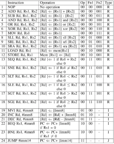
The VPRO is a 16-bit, 5-stage pipelined RISC processor. It has 24 most common instructions. It uses load/store architecture and consists of 8 general purpose 16-bit registers.
Instruction Set Architecture:
It consists of three types of instructions. 1) Register- Register type instructions
2) Immediate type instructions
3) Jump type instructions
The structural organization of the processor is shown in Fig. 7 and the instruction encoding is given in Table IV.
ACKNOWLEDGMENT
The authors would like to thank Dr. S. Ohtake and Dr. T. Yoneda of Nara Institute of Science and Technology for their valuable comments. They would also like to thank the STARC members for their valuable comments.
REFERENCES
[1] S. M. Thatte and J. A. Abraham, “Test generation for microprocessors,” IEEE Trans. Comput., vol. C-29, no. 6, pp. 429–441, Jun. 1980. [2] J. Shen and J. A. Abraham, “Native mode functional test generation
for processors with applications to self test and design validation,” in Proc. Int. Test Conf., 1998, pp. 990–999.
[3] K. Batcher and C. Papachristou, “Instruction randomization self test for processor cores,” in Proc. VLSI Test Symp., 1999, pp. 34–40. [4] L. Chen and S. Dey, “Software-based self-testing methodology for pro-
cessor cores,” IEEE Trans. Comput.-Aided Des. Integr. Circuits Syst., vol. 20, no. 3, pp. 369–380, Mar. 2001.
[5] N. Krantis, D. Gizopoulos, A. Paschalis, and Y. Zorian, “Instruction- based self-testing of processor cores,” in Proc. VLSI Test Symp., 2002, pp. 223–228.
[6] N. Krantis, A. Paschalis, D. Gizopoulos, and Y. Zorian, “Instruction- based self-testing of processor cores,” J. Electron. Testing: Theory and Appl. (JETTA), vol. 19, pp. 103–112, 2003.
[7] K. Kambe, M. Inoue, and H. Fujiwara, “Efficient template generation for instruction-based self-test of processor cores,” in Proc. IEEE Asian Test Symp., 2004, pp. 152–157.
[8] L. Chen, S. Ravi, A. Raghunath, and S. Dey, “A scalable software- based self-test methodology for programmable processors,” in Proc. Des. Autom. Conf., 2003, pp. 548–553.
[9] N. Krantis, G. Xenoulis, A. Paschalis, D. Gizopolous, and Y. Zorian,
“Application and analysis of RT-level software-based self-testing for embedded processor cores,” in Proc. Int. Test Conf., 2003, pp. 431–440. [10] A. Paschalis and D. Gizopoulos, “Effective software-based self-test strategies for on-line periodic testing of embedded processors,” in Proc. Des. Test Eur., 2004, pp. 578–583.
[11] W.-C. Lai, A. Krstic, and K.-T. Cheng, “On testing the path delay faults of a microprocessor using its instruction set,” in Proc. VLSI Test Symp., 2000, pp. 15–20.
[12] ——, “Test program synthesis for path delay faults in microprocessor cores,” in Proc. Int. Test Conf., 2000, pp. 1080–1089.
[13] W.-C. Lai and K.-T. Cheng, “Instruction-level DFT for testing pro- cessor and IP cores in system-on-a-chip,” in Proc. Des. Autom. Conf., 2001, pp. 59–64.
[14] V. Singh, M. Inoue, K. K. Saluja, and H. Fujiwara, “Instruction-based delay fault testing of processor cores,” in Proc. Int. Conf. VLSI Des., 2004, pp. 933–938.
[15] ——, “Delay fault testing of processor cores in functional mode,” IEICE Trans. Inf. Syst., vol. E-88D, no. 3, pp. 610–618, Mar. 2005. [16] A. Krstic and K.-T. Cheng, Delay Fault Testing for VLSI Circuits.
Norwell, MA: Kluwer, 1998.
[17] J. L. Hennessy and D. A. Patterson, Computer Architecture: A Quanti- tative Approach. San Mateo, CA: Morgan Kaufmann, 1996. [18] V. Singh, M. Inoue, K. K. Saluja, and H. Fujiwara, “Instruction-based
delay fault self-testing of pipelined processor cores,” in Proc. IEEE Int. Symp. Circuits Syst., 2005, pp. 5686–5689.
[19] ——, “Software-based delay fault self-testing of pipelined processor cores,” NAIST, Nara, Japan, (2004). [Online]. Available: http://isw3. naist.jp/IS/TechReport/report/2004006.ps
[20] S. Shamshiri, H. Esmaeilzadeh, and Z. Navabi, “Instruction-level test methodology for CPU core self-testing,” ACM Trans. Des. Autom. Electron. Syst., vol. 10, no. 4, pp. 673–689, Oct. 2005.
Virendra Singh (M’03) received the B.E. and M.E. degrees in electronics and communication engineering from Malaviya National Institute of Technology, Jaipur, India, in 1994 and 1996, respec- tively, and the Ph.D. degree in computer science from Nara Institute of Science and Technology (NAIST), Nara, Japan, in 2005.
He has been a Scientist at Central Electronics En- gineering Research Institute (CEERI), Pilani, India, since March 1997. Prior to this, he served as an As- sistant Professor at Banasthali University, Vanasthali, India, from June 1996 to March 1997. His research interests include design val- idation and test of high performance processors and fault tolerant computing.
Dr. Singh is a member of the ACM and a life member of the Institute of Electronics and Telecommunication Engineers (IETE) of India.
Michiko Inoue (M’95) received the B.E., M.E., and Ph.D. degrees in computer science from Osaka University, Osaka, Japan, in 1987, 1989, and 1995, respectively.
She worked at Fujitsu Laboratories Ltd., Kawasaki, Kanagawa, Japan, from 1989 to 1991. She is currently an Associate Professor of Graduate School of Information Science, Nara institute of Science and Technology (NAIST), Nara, Japan. Her research interests include distributed algorithms, parallel algorithms, graph theory, and design and test of digital systems.
Dr. Inoue is a member of the Institute of Electronics, Information, and Com- munication Engineers of Japan, the Information Processing Society of Japan, and Japanese Society for Artificial Intelligence.
Kewal K. Saluja(F’94) received the B.E. degree in electrical engineering from the University of Roorkee, Roorkee, India, in 1967, and the M.S. and Ph.D. degrees in electrical and computer engineering from the University of Iowa, Iowa City, in 1972 and 1973, respectively.
He is currently a Professor with the Department of Electrical and Computer Engineering at the University of Wisconsin-Madison, where he teaches courses in logic design, computer architecture, microprocessor-based systems, VLSI design and testing, and fault-tolerant computing. Prior to this, he was with the University of Newcastle, Newcastle, Australia. He has held visiting and consulting positions at various national and international institutions including University of Southern California, Los Angeles, CA, Hiroshima University, Hiroshima, Japan, Nara Institute of Science and Technology, Nara, Japan, and the Uni- versity of Roorkee. He has also served as a consultant to the United Nations Development Program. He was the general chair of the 29th FTCS and he served as an Editor of the IEEE TRANSACTIONS ONCOMPUTERS(1997–2001). He is currently the Associate Editor for the letters section of the Journal of Electronic Testing: Theory and Applications (JETTA).
Professor Saluja is a member of Eta Kappa Nu, Tau Beta Pi, and a fellow of the JSPS.
Hideo Fujiwara (S’70–M’74–SM’83–F’89) re- ceived the B.E., M.E., and Ph.D. degrees in electronic engineering from Osaka University, Osaka, Japan, in 1969, 1971, and 1974, respectively.
He was with Osaka University from 1974 to 1985 and Meiji University, Tokyo, Japan, from 1985 to 1993, and joined Nara Institute of Science and Tech- nology (NAIST), Nara, Japan, in 1993. He served as a Senator of NAIST from 1998 to 2000. Presently, he is a Professor at the Graduate School of Information Science, NAIST. His research interests include logic design, digital systems design and test, VLSI computer-aided design (CAD), and fault tolerant computing, including high-level/logic synthesis for testability, test synthesis, design for testability, built-in self-test, test pattern generation,
parallel processing, and computational complexity. He has authored seven books including Logic Testing and Design for Testability (MIT Press, 1985). He has also authored or coauthored more than 270 technical papers. He has served as an Editor of the IEEE TRANSACTIONS ONCOMPUTERS, Journal of Electronic Testing, Journal of Circuits, Systems, and Computers, Journal of Very Large Scale Integration (VLSI) Design, and others, and is an advisory member of IEICE Transactions on Information and Systems.
Dr. Fujiwara was a recipient of the IECE Young Engineer Award in 1977, IEEE Computer Society Certificate of Appreciation Awards in 1991, 2000 and
2001, Okawa Prize for Publication in 1994, IEEE Computer Society Meritorious Service Awards in 1996 and 2005, IEEE Computer Society Continuing Service Award in 2005, and IEEE Computer Society Outstanding Contribution Award in 2001. He is a Golden Core member of the IEEE Computer Society, a fellow of the Institute of Electronics, Information and Communication Engineers of Japan (IEICE), and a fellow of the Information Processing Society of Japan.