Bipartite Full Scan Design: A DFT Method for Asynchronous Circuits
Hiroshi Iwata†‡, Satoshi Ohtake†‡, Michiko Inoue†‡ and Hideo Fujiwara†‡
† Graduate School of Information Science, Nara Institute of Science and Technology 8916-5 Takayama, Ikoma, Nara 630-0192, Japan
‡ Japan Science and Technology Agency, CREST Email:{ hiroshi-i, ohtake, kounoe, fujiwara }@is.naist.jp
Abstract—A globally-asynchronous and locally-synchronous (GALS) system has been known as a realistic hardware design solution for many difficulties such as global clock network that arise due to the continuous scaling of semiconductor technology. Although a full scan design method for synchronous circuits is applied to asynchronous circuits to achieve the same testability of their combinational parts, the overhead is extremely high. To reduce the overhead, several variation of scan-based approaches have been proposed but they cannot guarantee complete test. In this paper, we propose a bipartite full scan design as a new DFT method for asynchronous circuit where we guarantee complete test for both combinational and sequential parts of circuits with area and performance overhead comparable to the previous best method in terms of overhead.
Keywords-Asynchronous circuit testing, L1L2* full scan de- sign, bipartite full scan design, scan C-element path
I. INTRODUCTION
A globally-asynchronous and locally-synchronous (GALS) system has been known as a realistic solution for many difficulties such as global clock network that arise due to the continuous scaling of semiconductor technology. Therefore, asynchronous circuits are required to have as high testability as synchronous circuits. In a GALS system, locally synchronized functional modules are connected with self-timed interconnects using asynchronous handshake communication protocols. The use of GALS design methodology eases reuse of legacy functional modules and simplifies timing closure between the modules. Furthermore, heterogeneous and variable clocking of the functional modules can be easily implemented in a GALS system and then reduction of power consumption of the whole system can be achieved. ITRS predicts that 25% and 45% of a design will be driven by handshake clocking in the year 2015 and the year 2022, respectively[1].
GALS systems compose of both synchronous and asyn- chronous parts, and therefore, asynchronous parts are re- quired as high testability as combinational parts. As a straightforward application of a synchronous DFT method to asynchronous circuits, Level Sensitive Scan Design (LSSD) for asynchronous circuits has been proposed[2]. The method inserts an LSSD scan element to every combinational loop to enable combinational test generation for the combinational kernels. Since the method requires insertion of a large
number of LSSD scan elements, it involves high area and performance overhead. To resolve these problems, several scan-based approaches have been proposed. These can be classified into two categories: partial scan and full scan. The partial scan approaches [3], [4] reduce the number of combinational loops to be broken and keep the kernel sequential. Efthymiou et al.[3] proposed a method of testing CHAIN communication channel by breaking only global feedback loops. Ohtake et al.[4] minimized the number of breaking points by considering the minimum feedback arc set of a circuit graph.
In [5], [6], [7], full scan design methods with lower hardware overhead than the LSSD method have been pro- posed. Beest et al.[5] have adopted the L1L2* scan design[8] where each combinational loop is broken by a single scan latch and a pair of consecutive latches in a scan path works as scan shift register latch (scan SRL). Since LSSD needs two latches for one scan element, the number of additional latches can be reduced to half. They also proposed a multiplexer-based scannable C-element for L1L2* scan design[6] to further reduce area and performance overhead. The method adds only one additional multiplexer on the combinational loop inside every C-element and inserts no latch on the functional paths. Moreover, Shi et al.[7] en- hanced the multiplexer-based scan C-element to test transi- tion faults.
The most important merit of full scan-based DFT methods for asynchronous circuits is that the well developed combi- national circuit testing can be applied with minor modifica- tion. The L1L2* scan designs [5], [6] have lower overhead but they cannot guarantee complete test for combinational part of an asynchronous circuit and do not support testing of the sequential part of the circuit. In this paper, we propose a new full scan design method based on L1L2* for C-element- based asynchronous sequential circuit and a new scannable C-element design. Our method has the following advantages: (1) complete test is guaranteed for the combinational part which cannot be achieved by the previous L1L2*-based full scan design method, (2) complete test is guaranteed for the sequential part which is not supported by any previous full scan design methods, and (3) performance overhead is comparable to the previous best method[6] in terms of overhead.
IEEE 19th Asian Test Symposium (ATS'10), pp. 206 - 211, December 2010.
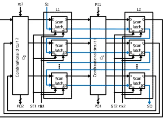
Figure 1. L1L2* scan design.
The rest of the paper is organized as follows. In Section II, we review the previous methods based on full scan and point out their limitations. Some preliminaries are introduced in Section III. Sections IV and V present our proposed DFT method on scan path configuration and a new scan C-element, respectively. Section VI concludes the paper.
II. RELATED WORKS
In this section, we first review the L1L2* scan design proposed in [8] as shown in Fig.1. For a circuit of single latch design [9], the combinational part of a circuit can be divided into two disjoint sub combinational circuitsC1and C2 and the set of all the latches are partitioned into two sub sets, L1 and L2, where latches in L1 drive onlyC1and are driven only byC2, and latches in L2 drive onlyC2and are driven only byC1. Latches in L1 and L2 are connected alternately to compose a scan path, and any pair of two consecutive latches in the scan path works as a scan SRL. For this design, test application for the combinational circuit is also divided into two stages, forC1andC2. Scan shift is operated by applying load and hold controls alternately to L1 and L2, respectively. By this scan shift, any values can be set to all the scan SRLs.
For asynchronous circuits, several scan elements which are used to break combinational loops have been proposed. If a scan SRL is inserted to every combinational loop in a circuit, any test pattern can be applied to the combinational part of the circuit by using the scan SRLs but the perfor- mance and area overhead are extremely high. The overheads can be also reduced by using the L1L2* scan design for the asynchronous circuits. Beest et al.[5] introduced the L1L2* scan design scheme to asynchronous circuits. In their method, a scan latch composed of a multiplexer and a latch is used to break a combinational loop. By inserting the scan latches to make an asynchronous circuit a single latch design and constructing scan SRL based on the L1L2* scan design scheme, any test pattern can be applied to each individual sub combinational circuit. Furthermore, to reduce performance overhead of a scan latch inserted to the internal
Figure 2. A capture conflict on a scan C-element.
Figure 3. Loop containing single latch in capture procedure.
loop of a C-element, Beest et al.[6] proposed a new scan C- element. In the scan C-element, a latch is placed outside the functional loop.
However, the existing methods cannot always guarantee test response capture due to capture conflict and the presence of combinational loops.
A state transition of a C-element depends on its state. Therefore, an appropriate value is required to capture a test response into the C-element. Since the next state is determined by a majority of two input values and its current state, for example, when the two inputs have1/0 and 0, a state 1 is required to capture the error. In this case, since the state of the previous scan element is0, the state is 0 and the error1/0 at one input cannot be captured. We call this situation a capture conflict. Figure 2 shows an example of the capture conflict. In [5], [6], this problem is not discussed, and some test response might not be captured.
The second problem on the existing method is presence of combinational loops. Multiplexer-based scan C-element can construct L1L2* scan design with low area and performance overhead. However, if this type of scan C-element is used in the L1L2* scan design, as proposed in [5], there may exist a loop with one latch, and it becomes a combinational loop if the latch is in the load mode in a capture process as illustrated in Figure 3. In this case, an oscillation may occur
and then the expected value is not guaranteed.
In this paper, for an asynchronous circuit, we propose a DFT method based on L1L2* scan design. In our pro- posed method, the problems of the capture conflict and the combinational loop are resolved, and complete test for both the combinational part and the sequential elements in the asynchronous circuit are guaranteed.
III. PRELIMINARIES
In this paper, we consider an asynchronous circuit which consists of only two-input C-elements and latches as its se- quential elements and a feedback free combinational circuit.
Definition 1 (Bipartite asynchronous circuit structure): For an asynchronous circuitC, C is bipartite asynchronous circuit structure if the combinational part of C is divided into two disjoint sub circuits C1 and C2, and the set of all the sequential elements of C are partitioned into two subsets, L1 and L2, such that sequential elements in L1 drive only C1 and are driven only by C2, and sequential elements in L2 drive onlyC2and are driven only byC1.
In this paper, we assume that a scan element has two modes, normal operation and scan operation. In scan opera- tion, the element operates as a latch i.e., the mode is further classified into load operation and hold operation.
Definition 2 (bipartite scan path): A scan pathp, which is a sequence of scan elements, is called bipartite scan path (B-scan path) if it satisfies the following conditions.
1) Scan elements onp are partitioned into two subsets. 2) Any two consecutive scan elements on p belong to
different sets.
3) All the scan elements in each set perform the same mode of operation simultaneously.
Definition 3 (S-graph): An S-graph G = (V, E) of an asynchronous circuit C is a directed graph, where a node v ∈ V represents a sequential element in C and an edge (u, v) ∈ E represents that a data output of u is a transitive fanin1of a data input ofv.
Definition 4 (Undirected cycle): For an S-graph, a cycle on the graph if the directions of all the edges are ignored is called an undirected cycle on the S-graph.
In this paper, an asynchronous circuit is tested by han- dling the combinational part and each individual sequential element separately. For a combinational circuit, we target the following logical faults. A logical fault of the combinational circuit changes the logic function of some output of the combinational circuit to some other logic function but does not include any other input variables and does not make the circuit sequential. Note that all the stuck-at faults in the combinational circuit can be represented by the logical faults. A combinational circuit is said to be completely tested
1A signal line l is said to be a transitive fanin of some other signal line m if there exists a combinational connection from l to m.
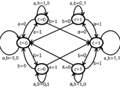
Figure 4. State diagram of a C-element.
if all the detectable logical faults of the combinational circuit can be detected.
For a sequential element, we target the following logical faults. A logical fault of a sequential element changes the logic function, i.e., the state transition function and/or output function, to some other logic function but does not include any other input variables and does not change states appeared in the state table. Note that all the stuck-at faults in a sequential element composed of standard gates can be represented by the logical faults. A sequential element is said to be completely tested if all the detectable logical faults of the sequential element can be detected.
Complete test of a combinational circuit can be achieved if, for each output of the circuit, any pattern can be applied to the inputs that are transitive fanin of the output and any response from the output can be observed.
Figure 4 shows the state diagram of a two-input C- element. There are 12 transitions and 6 stable states in the diagram. Complete test of the C-element can be achieved if every transition in the state diagram is examined, i.e., for each pair of a stable state and a pattern which is single input change of the input pattern of the stable state, observing the response from the C-element by setting the stable state and applying the pattern. A latch is also a two input sequential element. Complete test of latches can be achieved by the similar way as testing of the C-element.
IV. BIPARTITE FULL SCAN DESIGN
In this section, we assume that scan elements consist of scan latches and scan C-elements where a scan C-element is single latch type proposed in [5] or the one proposed in Section V.
To resolve the capture conflict, we introduce a new testability for asynchronous circuits. As we mentioned, to capture an error at some C-element, the C-element has to have some appropriate value. We call the value a capture pattern. The testability requires that for any two consecutive scan C-elements si and si+1 in a scan path, there is no combinational connection from si to si+1. This condition allows a test pattern to detect a fault and its corresponding capture pattern to be controlled independently.
Definition 5 (bipartite full scan testability): For an asyn- chronous circuit C, C is bipartite full scan (BF-scan) testableif it satisfies the following conditions.
1) Every sequential element inC is a scan element. 2) C has at least one scan paths and each sequential
element is included in some scan path.
3) C is bipartite asynchronous circuit structure and com- posed of combinational sub circuits C1 and C2 and sets of sequential elements, L1 and L2.
4) Each scan pathp = s1, . . . , si, . . . , snis a B-scan path in terms of the sets L1 and L2.
5) For each pair of scan elements si and si+1 (i = 1, . . . , n − 1) on p, the data output of si is not a transitive fanin of the data input ofsi+1 inC. . The scan path p satisfying the conditions 4) and 5) is called a bipartite full scan (BF-scan) path.
Theorem 1: For an asynchronous circuitC, the combina- tional part of C can be completely tested if C is BF-scan testable.
Proof: Let C1, C2, L1 and L2 be sub circuits and sets of sequential elements described in Condition 3) of Definition 5. Letf be a detectable logical fault in C and f is related to an outputo. Let si be a scan element connected to o. If there is a scan element si+1 next to si in a scan path, si and si+1 have the same value after shifting in a test pattern off , and values of other scan elements can be controlled independently fromsi. From the definition, there is no combinational connection fromsi+1andsi. Therefore, the values of si and scan elements connected to transitive fanins of o can be controlled independently. For the test pattern, specified values are required only at the transitive fanins. Therefore, the test pattern and its capture pattern for si can be controlled independently. The captured response can be shifted out using the property of the B-scan path. Thus the theorem holds true.
A. Test generation method for the combinational part A test pattern for each fault on the sub circuit of an asynchronous circuit can be generated by a commercial combinational ATPG tool and its capture pattern can be obtained for the fault by a commercial fault simulation tool. For facilitating test application, we can reduce the number of test patterns as follows. By using the test pattern and capture pattern pair for a fault, some other faults may be detected. It can be examined by the fault simulation tool and the detected faults can be removed from the fault list. Moreover, several test pattern and capture pattern pairs can be applied simultaneously if these patterns are compatible with each other.
B. Proposed DFT method
In this subsection, we propose a DFT method which makes an asynchronous circuit BF-scan testable. First, we formulate the DFT problem as follows.
Definition 6 (DFT for BF-scan testability):
Input: An asynchronous circuitC and the number of scan paths
Output: A BF-scan testable circuit which has the same function ofC.
Optimize: Minimize the number of additional latches. To solve the problem, we propose an algorithm which consists of the following three steps.
1) Every sequential element of C is replaced with its corresponding scan element.
2) The S-graph of the above circuitC is transformed to a bipartite graph ofGb= (V1, V2, E).
3) BF-scan paths are constructed.
i) Transformation from S-graph to bipartite graph: A bipartite graph is required that a length of every undirected cycle in the S-graph is even. In Step 2), we insert the minimum number of additional latches at the output of scan elements to transform the S-graph to a bipartite graph. Since the additional latches affect the performance of the normal operation, we minimize the number of the additional latches. The scan elements whose outputs have additional scan latches are determined by solving the following integer programming.
Minimize:
!n i=1
δi
Subject to:For each undirected cyclecj (j = 1, . . . , m),
!n i=1
[(1 + δi) × INi,j] = 2 × "j
1 ≤ "j≤n
wheren is the number of vertices in an S-graph, variable δi
(i = 1, . . . , n) is a Boolean variable to express the addition of a latch to the output of vi, m is the number of the undirected cycles in the S-graph, "j is an integer variable, and a coefficient INi,j(= 0, 1) indicates that vi belongs to cj if its value is1 and vice versa.
ii) Construct BF-scan paths: In Step 3), BF-scan path is constructed by using the bipartite S-graph obtained in the previous step. First, we define the compatibility graph as follows.
Definition 7 (Compatibility graph): For a bipartite S- graphGb= (V1, V2, Eb), the graph Gc= (V, Ec) is referred as the compatibility graph of Gb, where V is the set of verticesV1∪V2and(u, v) ∈ Ecis an edge betweenu, v ∈ V means that v is not adjacent to u and u is in V1 (resp.V2) ifv is in V2 (resp.V1) inGb.
Here, we describe the algorithm to construct BF-scan paths by using bipartite S-graphGb = (V1, V2, Eb) and its compatibility graphGc= (V, Ec).
1) For each scan path, select a scan element as the beginning of the scan path.
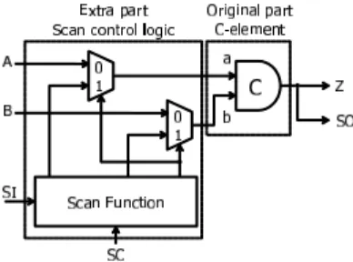
Figure 5. Gate level implementation of the proposed scan C-element.
2) For each scan path, select a scan element, whose corresponding vertex is adjacent to the vertex corre- sponding to the previously selected scan element in the compatibility graph, as the next scan element in the scan path. If there exists no selectable scan element, a new scan latch which is not connected to the circuit is added to the circuit, and the compatibility graph is updated.
3) Repeat Step 2) until all vertices are selected. Update operation of the compatibility graph is adding a new vertexv to V and if the previous scan element belongs to V1 (resp.V2), edges from x to all the vertices in V1 (resp. V2) are added to Ec.
Since the additional latches constructing the BF-scan path do not affect the performance of the normal operation, the number of additional latches is not minimized in this Step. The number of latches added in this step may be small for a large asynchronous circuit because independent scan elements may be sufficiently available for selecting one as the next scan element in Step 2).
V. SCANNABLEC-ELEMENT DESIGN AND TESTING SCAN PATH
A. Scannable C-element design
In this section, we propose a novel scannable C-element where we use the C-element’s bistability itself as a memory element for scan paths. By utilizing the bistability of C- elements, our proposed scan C-element has the following two important features: (1) every C-element on the scan paths can be completely tested by invoking any state transi- tion using consecutive single input change patterns, and (2) the performance overhead of the proposed scan C-element is the same as that of the multiplexer-based one which has the smallest delay overhead so far.
Figure 5 shows the block diagram of the proposed scan C-element. The structure of the proposed scan C-element consists of two parts, the original part (C-element) and the extra part (scan control logic). For this design, any type of C-element can be used in the original part. Scan control logic is a combinational circuit whose function is shown in Table I. The function of scan control logic has three
Table I
THE TRUTH TABLE OF SCAN CONTROL LOGIC SC a b Function
00 A B Normal operation (capture) 01 0 1 Scan operation (hold) 10 1 0 Scan operation (hold) 11 SI SI Scan operation (load)
types of operations: (1) normal operation which is used in normal mode of the circuit and capture mode during test, (2) hold operation which is used to preserve the internal state of the C-element, and (3) load operation which is used to load the value on SI into the proposed scan C- element. The details of the scan control logic are described as follows. Operation (1) switches the scan C-element to the normal operation by applying SC=00. Operation (2) can be performed by applying (a,b)=(0, 1) or (a,b)=(1, 0) to the C-element by applying SC=01 or SC=10, respectively. The pattern (a,b)=(0, 1) or (a,b)=(1, 0) is referred as a hold pattern. We can avoid any race on the capture process with the proposed scan C-element by choosing one of the hold pattern. The details are discussed in the next subsection. Operation (3) loads the value of SI into the C-element by applying SC=11.
B. Race avoiding method in capture procedure
In this subsection, we propose a method to avoid a race in the capture process.
For the proposed scan C-element, we can choose hold function from (a,b)=(0, 1) and (a,b)=(1, 0). Suppose that (a,b)=(0, 1) is applied to the C-element to preserve the internal state and the internal state is 1. If a response (A,B)=(1/0, 0) is propagated to the input of the C-element and scan control is switched from “hold” to “capture”, the internal state of the C-element may not become an intended state because the internal state becomes1/0 if the value at A reaches earlier than B. Otherwise, the internal state becomes 0.
However, we can avoid such a race by applying (a,b)=(1, 0) to the C-element as the hold operation because the internal state of the C-element becomes 1/0 even if either of the values at A and B reaches earlier than the other. Therefore, we can avoid any race by selecting the hold operation based on the propagated response to the proposed scan C-element. The desired value of the race free hold operation for the C-element can be determined by running fault simulation during test generation. Even if we omit the fault simulation, any response can be captured by applying the test pattern for one of the hold operation (a,b)=(0, 1) and repeating the same test patterns for the other hold operation (a,b)=(1, 0).
C. Testing of proposed scannable C-element in b-scan path To test the C-element, it is necessary to apply some specific test sequence and capture the response. As a feature
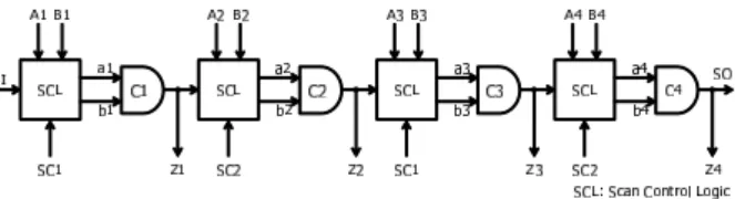
Figure 6. The scan path part of the micropipeline with proposed scan C-element
of the proposed scan C-element, an arbitrary two consecutive patterns with single input change can be applied to any C- element on the B-scan path. Moreover, the responses of the C-elements can be observed through the B-scan path where the test sequence is applied.
Figure 6 shows a B-scan path constructed with four proposed scan C-elements. To test C-elements in B-scan path, any response is necessary to be observed at SO where the response is obtained by setting specific stable states and applying test patterns to the C-elements. We classify the transitions of the C-element into three types, no output change (NOC), output flush (OF) and output change (OC). An NOC transition occurs when the output is maintained by holding the internal value of the C-element, i.e., there are four transitions, (a,b,c)=(0, 0, 0) → (0, 1, 0), (0, 0, 0) → (1, 0, 0), (1, 1, 1) → (0, 1, 1) and (1, 1, 1) → (1, 0, 1), where c is the internal value of the C-element. An OF transition occurs when the output is maintained by loading the same value of the internal value, i.e., there are four transitions, (a,b,c)=(0, 1, 0) → (0, 0, 0), (1, 0, 0) → (0, 0, 0), (0, 1, 1) → (1, 1, 1) and (1, 0, 1) → (1, 1, 1). An OC transition occurs when the output is changed by loading the different value from the internal value, i.e., there are four transitions, (a,b,c)=(0, 1, 0) → (1, 1, 1), (1, 0, 0) → (1, 1, 1), (0, 1, 1) → (0, 0, 0) and (1, 0, 1) → (0, 0, 0).
To test an NOC transition(0, 0, 0) → (0, 1, 0), we operate the following two steps. (1) Initialize all the C-elements to 0 in B-scan path by applying SC1=SC2=11 and SI=0. (2) Operate scan shift with SI=0 and 01 to SC1 (resp. SC2). By using the hold pattern (a,b)=(0, 1), the transition is applied to every C-element in L1 (resp. L2) and the responses are captured at L2 (resp. L1) by applying consecutive patterns 11, 01 to SC2 (resp. SC1). Since the captured values are used as scan in of next scan C-elements, the erronous value can be shifted out to SO. Other NOC transitions are tested as the same manner by changing the combination of hold patterns and SI values.
To test an OF transition(0, 1, 0) → (0, 0, 0), we operate the following three steps. (1) Initialize all the C-elements to 0 in B-scan path by applying SC1=SC2=11 and SI=0. (2) Apply the hold pattern (a,b)=(0, 1) to all the C-elements by applying SC1=SC2=01 and SI=0. (3) Initialize all the C- elements to0 by applying SC1=SC2=11. If there is an error on the transition (0, 1, 0) → (0, 0, 0) at some C-element,
the subsequent C-elements are load the erroneous value and propagate to SO.
To test an OC transition (a,b,c)=(0, 1, 0) → (1, 1, 1), we operate the following three steps fori-th C-element in the B- scan path. (1) Initialize all the C-elements to0 in the B-scan path by applying SC1=SC2=11 and SI=0. (2) Operate scan shift with SI=1 and SC1=01, 11 and SC2=11, 00 and vice versa until (a,b)=(1, 1) is applied to i-th scan C-element. (3) Initialize all the C-elements to1 by applying SC1=SC2=11. The transition is applied to i-th scan C-element since the situation ofi-th scan C-element was (0, 1, 0) before applying the load pattern(1, 1). Therefore, the erronous value can be propagated to SO like OF transitions.
D. Experimental result
In this subsection, we evaluate the testability and the overhead of the proposed scan C-element and compare it to the previous design including multiplexer-based scan C- element, introduced in [6].
All the proposed scan C-elements in the B-scan path are tested completely with the method discussed in Section V-C. On the other hand, any existing scan C-element in B- scan path can not be tested. To test the C-element in an existing scan C-element, it is needed for testing with setting
“scan enable” off, i.e., it is not practical because the C- elements are tested in the circuit without using the scan path. Furthermore, it is difficult to achieve complete test even if it is possible.
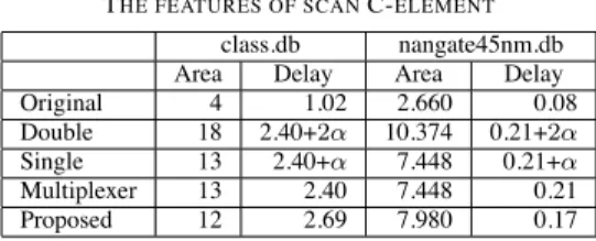
We have implemented several types of the scan C- elements with standard cells and combinational loops. We used Synopsys Design Compiler C-2009.06 as a logic syn- thesis tool and 2 types of technology library, class.db and nangate45nm.db. Class.db and nangate45nm.db are standard cell libraries whose areas of a nand gate are 1 and 0.798, respectively. Since there is no information of the delay about the latch in the libraries, we referred the delay of the latch as α. Table II shows the results of logic synthesis. Columns
“Area” and “Delay” under “class.db” and “nangate45nm.db” mean that the area of scan C-element and the delay of the normal operation, respectively. Rows “Original”, “Dou- ble”, “Single”, “Multiplexer” and “Proposed” mean that the synthesis results of original C-element, double latch type scan C-element, single latch type of scan C-element, multiplexer-based scan C-element, and our proposed scan C-element. From the experiment, proposed scan C-element can be completely tested with low overhead comparable to the conventional approaches.
VI. CONCLUSION
L1L2* scan design methods proposed for asynchronous circuits do not guarantee the complete test because there may exist dependency between a test pattern and its capture pattern. In this paper, we have introduced bipartite full scan (BF-scan) testability to remove the dependency affecting
Table II
THE FEATURES OF SCANC-ELEMENT class.db nangate45nm.db
Area Delay Area Delay
Original 4 1.02 2.660 0.08
Double 18 2.40+2α 10.374 0.21+2α
Single 13 2.40+α 7.448 0.21+α
Multiplexer 13 2.40 7.448 0.21
Proposed 12 2.69 7.980 0.17
complete test and we propose a DFT method that makes an asynchronous circuit BF-scan testable.
Moreover, we have proposed a new scan C-element using C-elements’ bistability themselves as memory elements of scan paths. All the C-elements on the bipartite scan path constructed with our proposed scan C-element can be tested with any single input change transition. Experimental result shows the proposed scan C-element can be implemented with low hardware and performance overhead. By using BF- scan testability and proposed scan C-element, asynchronous circuits can be tested completely.
ACKNOWLEDGMENT
The authors would like to thank Prof. Tomokazu Yoneda of Nara Institute of Science and Technology for valuable discussion and cooperation. This work was supported in part by Japan Society for Promotion of Science (JSPS) under Grants-in-Aid for Scientific Research (B) (No. 20300018).
REFERENCES
[1] “International technology roadmap for semiconductors 2007 edition: Design,” 2007.
[2] H. Hulgaard, S. M. Burns, and G. Borriello, “Testing asyn- chronous circuits: a survey,” Integr. VLSI J., vol. 19, no. 3, pp. 111–131, 1995.
[3] A. Efthymiou, J. Bainbridge, and D. A. Edwards, “Test pattern generation and partial-scan methodology for an asynchronous SoC interconnect,” IEEE Trans. VLSI Syst., vol. 13, no. 12, pp. 1384–1393, 2005.
[4] S. Ohtake and K. K. Saluja, “A systematic scan insertion technique for asynchronous on-chip interconnects,” in Digest of papers of Workshop on Low Power Design Impact on Test and Reliability (LPonTR), May 2008.
[5] F. te Beest, A. Peeters, K. Van Berkel, and H. Kerkhoff,
“Synchronous full-scan for asynchronous handshake circuits,” J. Electron. Test., vol. 19, no. 4, pp. 397–406, 2003. [6] F. te Beest and A. Peeters, “A multiplexor based test method
for self-timed circuits,” in Proc. of 11th IEEE International Symposium on Asynchronous Circuits and Systems, 2005, pp. 166–175.
[7] F. Shi and Y. Makris, “Testing delay faults in asynchronous handshake circuits,” in Proc. of 2006 IEEE/ACM international conference on Computer-aided design, 2006, pp. 193–197.
[8] S. DasGupta, P. Goel, R. G. Walther, and T. W. Williams, “A variation of lssd and its implications on design and test pattern generation in VLSI,” in Proc. of Test Conf., 1982, pp. 63–66. [9] M. Abramovici, M. A. Breuer, and A. D. Friedman, Digital Systems Testing and Testable Design. Wiley-IEEE Press, 1994.