Fast and Effective Fault Simulation for Path Delay Faults Based on
Selected Testable Paths
∗Dong Xiang
School of Software, Tsinghua University, Beijing 100084, China
Yang Zhao
Dept. of Comp. Sci. Tsinghua University Beijing 100084, China
Kaiwei Li
Dept. of Comp. Sci. Tsinghua University Beijing 100084, China
Hideo Fujiwara
Graduate Sch. of Inform. Sci., Nara Inst. of Sci. and Techn. Ikoma, Nara 630-0101, Japan
Abstract — Test generation and fault simulation of path delay faults are very time-consuming. A new fault simulation method of fully enhanced scan designed cir- cuits is proposed for path delay faults based on single stuck-at tests without circuit transformation. The pro- posed method identifies robustly and non-robustly testable paths first, for which a selected path circuit (SPC) is con- structed. The SPC circuit contains no internal fanouts. Fault simulation of non-robustly testable paths is reduced to 3-valued logic simulation of the SPC circuit. Fault sim- ulation is completed on the SPC circuit by only tracing the active part of SPC circuit. An effective fault dropping tech- nique is also adopted based on the selective tracing scheme. The proposed fault simulation scheme is extended to that of robustly testable path delay faults. Experimental re- sults confirm that the proposed fault simulator is exact. It is shown according to experimental results that the pro- posed fault simulator gets exact fault simulation results in very short time. Sufficient experimental results are pre- sented to compare with previous methods on CPU time and accuracy.
Keywords —Fault simulation, non-robust testing, path delay faults, robust testing, selected path circuit.
I. Introduction
Path delay fault test pairs can detect a lot of defects that cannot be discovered by the single stuck-at fault tests. Test generation and testing of path delay faults attract much attention. One of the most important problems for test generation of path delay faults is the huge number of paths in the circuit, which can increase exponentially with the size of the circuit. It is observed that most of the path delay faults in a circuit are usually redundant. It is unnecessary to spend much effort on test generation and fault simulation of the redundant path delay faults [2, 9]. Recently, a very good structure called zero-suppressed binary decision diagram is used to select testable or critical paths in reasonable time [12].
Enough methods have been proposed to handle test gen- eration of path delay faults by the single stuck-at fault test generation techniques [11, 14, 18]. However, circuit trans- formation is required for methods in [11, 14], which makes them unable to handle large circuits. Xiang, et al. [18] proposed a test generation method based on stuck-at tests, which presents a compact test set for complete coverage in reasonable time. The test generation method in [18] does not need to transform the circuit unlike many previous methods.
∗This work was partially supported by the National Science Foundation of China under grants 60373009 and 60425203.
Fault simulation for path delay faults has been studied extensively [4, 5, 6, 7, 13, 16, 17], which contributes to most of the CPU time to generate path delay fault test pairs. Schultz, Fink and Fuchs [16] proposed a parallel fault sim- ulation method for fault simulation of path delay faults. Non-enumerative fault simulation of path delay faults at- tracts a lot of attention. Pomeranz and Reddy [13] pro- posed the first non-enumerative fault simulation method in polynomial time of the circuit size. Several levels of approximation with increasing accuracy and complexity were also presented all in polynomial time of the circuit size. An exact non-enumerative fault simulator was pro- posed by Gharaybeh, Bushnell, and Agrawal in [5] based on the path-status graph, which is suitable for fault simu- lation of path delay faults for large circuits. Kagaris and Tragoudas [7] proved that the non-enumerative fault sim- ulation problem of path delay faults is NP-hard.
The proposed method selects non-robustly testable or robustly testable paths first, and a selected path circuit (SPC) is constructed based on the selected path set. Test pairs of path delay faults are obtained from single stuck-at fault tests. The SPC circuit contains no internal fanout. Fault simulation reduces to logic simulation of the original circuit, where the SPC circuit is searched exhaustively. An effective fault dropping technique is also adopted with a backward selective tracing scheme by effectively pruning the SPC circuit. The proposed method is suitable for fault simulation of both robust and non-robust test pairs of path delay faults. Experimental results show that the proposed fault simulator (called FastExact) is very fast compared to two non-enumerative fault simulators. The FastExact fault simulator presents exact fault simulation.
In the rest of this paper, preliminaries of the paper are presented in Section 2. A new fault simulation scheme based on forward logic simulation and the SPC circuit is proposed in Section 3. A new procedure to construct an SPC circuit that contains fanouts only at the inputs of the SPC circuit is proposed in section 4. An interesting fault simulation scheme is proposed in Section 5 by using a backward selective tracing scheme to drop faults. The fault simulation method is extended to robust test fault simulation in Section 6. Experimental results are presented in Section 7. The paper is concluded in Section 8.
II. Preliminaries
Let g1-g2- . . . -gn be a path p, and gi(v) be the value of gate gi when applying the test vector v to the circuit, where g1 and gn are primary input and primary output, respectively. The off-inputs of f (gi, p) are the inputs of gi
that are not gi−1. The path can have a rising or falling
Paper 26.2 INTERNATIONAL TEST CONFERENCE 1
U1
U
s 0 s
s 0 s 1
U0
1 xx
x0 x1
Figure 1: The Hasse diagram of the 10 values of the logic system.
1
2
3
4
5
6
7
9
(a)
7 1
73
72 0 0 0
{a2/0, b2/0}
{a3/0, b3/0}
81
{a2/0, b2/0}
1 0 6
1
{a1/0, b1/0} {a1/0, b1/0}
b 2 2
3
4
5 b3
(b) 82
1
1
1 a 2
b1 a 1 1 1
a 3
1
9{a3/0, b3/0}
{a2/0, b2/0, a3/0, b3/0}
1
10
{a1/0, b1/0}
11 8
10
11
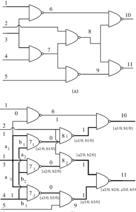
Figure 2: Example circuit fault simulation by logic simulation: (a) the original c17, (b) the full transfor- mation of c17.
transition at g1. A path p is a path delay fault if propaga- tion time of the rising or falling transition through the path exceeds a limit. Falling transition and rising transition at the source node of a path p are pf and pr, respectively.
Let cv and ncv be the controlling value and the non- controlling value of a gate. The definition for a robust test pair is directly obtained from [9].
Definition 1 Let f denote the on-input to gate g in the target path. Let h denote an off-input to gate g. The off- input h is called robust off-input with respect to an input vector pair V if:
• there is a cv → ncv transition or stable non- controlling value on h when the on-input f has a cv → ncv transition, and
• there is a non-controlling value on h when the on- input f has a ncv → cv transition.
Definition 2 A path delay fault for which there exists an input vector pair such that it activates the required transi-
construct-select-path-circuit()
1. Add the first path p in P into the SPC circuit, and delete p from P .
2. While P 6= ∅, for each p ∈ P , do
(a) Check nodes of p from the input to the out- put. Just put the node into SPC if it is not in SPC. If a node l of the path has been con- tained in SPC, put the predecessor of the node l in the path as an input of the gate whose output is l.
(b) Check the path p from l to the end, if the suc- cessor l′of l is still contained in the SPC, just go ahead; otherwise, generate a new fanout at the current node with node l feeding the gate l′ if l′ is not contained in SPC.
(c) Continue the process in steps a and b until reaching the output of path p.
3. For any node l in the original circuit that is not contained in the SPC, add l into SPC as an input of a gate if l is an input of a gate that is contained in both the original circuit and SPC, add l to the circuit as the input of the gate.
Figure 3: Selected path circuit construction for fault simulation.
tions on the path and all off-inputs in the path are robust off-inputs is called a robust testable path delay fault.
A non-robust test guarantees detection in the case of a single path-delay fault [5, 4, 3]. Therefore, a path de- lay fault for which there exists a non-robust test is called singly testable. The conditions for a non-robust test pair (v1, v2) are, (1) transition (with the appropriate direction ) is launched at the primary input of the target path, that is, for any on-path line g, we have g(v1) 6= g(v2); (2) for each gate along the target path, all off-inputs along the path have non-controlling values under v2.
We can generate test pairs of path delay faults for fully enhanced scan designed circuits without any circuit trans- formation. For any target path, a new circuit (called equiv- alent test generation circuit, ETGC) can be constructed as follows: The new circuit includes the original circuit in addition to another copy of the target path, where all off-input lines of the target path are connected with the corresponding lines in the original circuit. Test generation of the target path delay fault is equivalent to test genera- tion of the single stuck-at fault at the source node of the additional path as presented in [18].
As for the robustly testable path delay faults, the fault simulator and the test generator is implemented based on the 10−valued logic system. The 10-valued logic system [3] contains s0 (0,0), s0 (1,0), s1 (0,1), s1 (1,1), x0 (x,0), U, x1(x,1), U0, U1, and xx. Figure 1 presents the Hasse dia- gram of the 10-valued logic system. Let value a and b be connected, and a be the predecessor in the Hasse diagram.
We have value a contains value b. For example, x0 contains both s0 and s0, U1 contains U and x1, and x1 contains s1 and s1. The equivalent test generation circuit (ETGC) for a path can be constructed as follows: The target path in the ETGC circuit as mentioned above is replaced by one or more SPC circuits. For each gate in an SPC circuit, the ex- tra nodes of the gate are connected with the corresponding nodes in the original circuit. Test generation of a testable path delay fault is reduced to test generation of the single stuck-at fault at an input or a fanout branch of an input in the extra SPC circuit. Note that all inputs inside the extra SPC circuit are connected to the corresponding in- puts in the original circuit. This technique can completely simplify test generation for path delay faults. However, fault simulation is still handled in the corresponding SPC circuit based on the selective backtrace technique via logic simulation that is introduced later in this paper.
Accuracy of a fault simulator is very important. We call a fault simulator exact if it produces no simulation error in the process of fault simulation. That is to say, the fault simulator detects all path delay faults and only those faults that are detectable by the test pair set. The proposed fault simulator is an exact one, the exactness of which is confirmed experimentally in Section 7.
III. Forward Fault Simulation
We introduce a new method for fault simulation of path delay faults based on forward logic simulation and the SPC circuit. It is shown that fault simulation for circuits with- out internal fanout can be completed by using a logic sim- ulation scheme. While it is impossible to transform a cir- cuit completely when the circuit contains a huge number of paths, we present a new scheme by constructing an SPC circuit that contains only the selected critical and testable paths.
Figure 2(b) presents the full transformed circuit of the original circuit as shown in Figure 2(a). Logic values of all nodes corresponding to the test vector (1,2,3,4,5) = (0,1,1,1,1). It is clear that the test vec- tor can detect single stuck-at faults a1/0, b1/0, a2/0, b2/0, a3/0 and b3/0. Therefore, the test vector pair (1,2,3,4,5) = (00, 11, 01, 01, 11) covers path delay faults {p1/r, p2/r, p3/r, p4/r, p5/r, p6/r}, where p1, p2, p3, p4, p5 and p6are paths 3 − 7 − 8 − 10, 4 − 7 − 8 − 10, 3 − 7 − 8 − 11, 4 − 7 − 8 − 11, 3 − 7 − 9 − 11 and 4 − 7 − 9 − 11, and p/r represents the rising transition on a path.
However, there exist a large number of path delay faults that are untestable. These untestable faults can make the size of the transformed circuit very large. Repeated fault simulation on the untestable path delay faults is very time- consuming. It is quite good if the untestable paths are deleted from the transformed circuit, which can reduce the size of the transformed circuit greatly.
To solve the above problem, an SPC circuit is con- structed based on the selected critical and testable paths for fault simulation of path delay faults. The selected crit- ical and testable paths construct a simplified circuit that can still contain enough number of reconvergent fanouts of the original circuit. The SPC circuit is transformed into a fanout-free one by moving all fanouts to the inputs of the circuit. The SPC circuit has acceptable size because the number of critical paths is much less than that of the total paths in the original circuit.
forward-fault-simulation-by-logic-simulation()
1. Do logic simulation on the original circuit. 2. For each primary input i without fanout, it corre-
sponds to a path p. P (i) = {p/f } if i is assigned value 0, and P (i) = {p/r} if i is assigned value 1. For each fanout branch at the primary input i, it corresponds to a path p, P (i) = {p/f } if i is assigned value 0, and P (i) = {p/r} if i is assigned value 1.
3. For each gate g with inputs i1, i2, . . . , ik, P (g) =
∪jP (ij), where all other inputs it (t 6= j) are as- signed the sensitization value by the test vector. 4. For any inverter g with input i, P (g) = P (i). 5. Continue the above process until reaching the out-
puts of SPC circuit. The test vector pair covers faults ∪iP (i), where i is an output of the circuit.
Figure 4: Replacing fault simulation by logic simula- tion.
The procedure to construct the SPC circuit as presented in Figure 3 is based on the selected path set P . The first path is put into the SPC circuit directly. For each of the remaining paths, check from the source node. Just put the node into the circuit if it is not found in the SPC circuit. Put the predecessor of the node l in the path as an input of the gate whose output is l in SPC circuit if node l has been in the SPC circuit. Continue the above process until a node l′of the path is found not in the SPC circuit. Let l be the predecessor of l′in the path, which has been in SPC circuit. Generate a fanout at l, where the fanout branch feed gate l′. Our method can construct an SPC circuit based on any subset of testable paths. This feature of the procedure presented in Figure 3 is very attractive.
Some nodes in the original circuit may be not contained in the SPC circuit based on the selected testable and crit- ical paths. Nodes in the original circuit that are not con- tained in the SPC circuit and feed to one gate of the SPC circuit should be added. These nodes, called extra nodes of the SPC circuit, are added to the circuit. The constructed SPC circuit may contain some internal fanouts, which is transformed into one with no internal fanouts.
Fault simulation can be handled on the transformed SPC circuit with the logic-simulation-based scheme pre- sented in Figure 4. Logic simulation on the original circuit is used for a given test vector to get values of the extra nodes in the SPC circuit. It is necessary for the procedure presented in Figure 4 to get values of those extra nodes for the given test vector. Let P (i) be the sensitized path set that contains gate i in the SPC circuit. The sensitization value of an AND or NAND gate is 1, and 0 for an OR or NOR gate. Each path from the primary input (or pseudo primary input) or a fanout branch of a primary input has only one path leading to a primary output (or pseudo pri- mary output). The proposed procedure checks each path from its input to the output. It is detected by the test vec-
2
3
4 5 1
1 1 1
0
1
7 2
3
4 7
7 1
3
2
5
(a) 1
81 1
82
(b) 1
1
1 1
1 1 1
0 1
0
0
0
9
11 10 11 10
8
7
9
6 6
Figure 5: The SPC circuit: (a) the SPC circuit of c17, (b) the full transformation of the SPC circuit.
1 2 n
1 m
2 1
2 3
(a) (b)
1 2
(c)
3 1 2
(d) b
b b b
i i i
a b c
a b d
d d d
{ }a { }a,b,c { , }
d d d d d
a b c a b c a b c
b
a a b c
( )d3
a
Figure 6: Useless paths in the SPC circuit: (a) General structure, (b) an example, (c) the transformed circuit of 6(b), and (d) the actual transformed circuit.
tor if all off-inputs of the path are assigned sensitization values. The covered paths are kept in P (i) after running the procedure in Figure 4, where i is a primary output (or pseudo-primary output). Different outputs keep separate detected path sets.
Let us consider the circuit as shown in Figure 2(a) again, and the following paths be selected as critical paths: {3- 7-8-11, 3-7-9-11, 4-7-9-11, 4-7-8-11, 3-7-8-10, 4-7-8-10 } = {p1, p2, p3, p4, p5, p6}. Figure 5(a) presents the SPC of c17 according to the procedure in Figure 4 and the given criti- cal path set. Figure 5(b) gives the fully transformed circuit of the SPC circuit in Figure 5(a). Our method gets the values of all extra nodes based on logic simulation on the original circuit corresponding to a test vector. As shown in Figure 5(a), our method gets value of the extra node 6 based on logic simulation for the original circuit. The same results as that presented in Figure 2 can be obtained. Test vector 01111 covers single stuck-at faults a1/0, a2/0, a3/0, b1/0, b2/0, and b3/0. And test pairs (1,2,3,4,5) = (00, 11,
construct-fanout-free-SPC()
1. While one path in P has not been handled, do steps 2, 3, 4, 5, 6, and 7.
2. Add the first path p ∈ P into the SPC circuit, and delete p from P . For each path p ∈ P , check whether the fanout at the primary input has been in the SPC circuit. If so, exit; otherwise, do 3, 4, 5, 6, and 7.
3. Check whether all fanouts contained in p (corre- sponding to the original circuit) have been in the SPC circuit. If so, 6 and 7.
4. At least one fanout in p has been in the SPC cir- cuit, check whether path p has the same fanout branch in the original circuit. If not, exclude the path p.
5. Check path p from the input to the output, if one gate l of the path has been in the SPC, put the predecessor of the node l in path p as an input of gate l in the SPC.
6. Just put each node of path p into the SPC if it is contained in the SPC. If one gate l of the path p has been in the SPC, put the predecessor of the node l in path p as an input of l.
7. For each new fanout added to the SPC, record the corresponding branch number in the original circuit.
8. For each node l that feeds a gate of the SPC in the original circuit, add l to the gate as an extra line. If P is empty, end. Otherwise, go to step 1.
Figure 7: Constructing a fanout-free SPC circuit.
01, 01, 11) covers path delay faults {p1/r, p2/r, p3/r, p4/r, p5/r, p6/r}.
IV. Constructing Fanout-Free SPC Circuits The transformed SPC circuit may contain some paths that are not contained in the selected path set. Figure 6(a) presents the general structure of the SPC circuit. There ex- ist at least max(n, m) selected testable paths to construct the SPC as shown in Figure 6(a). There exist n·m paths in the transformed circuit, where some of them may not be re- ally the selected testable or critical paths. As shown in the example in Figure 6(b), Figure 6(c) shows the transformed circuit, and Figure 6(d) presents the actual transformed circuit. Therefore, it is not good to transform the SPC circuit directly. It is necessary to exclude those paths that are not contained in the selected path set.
We would like to introduce a new procedure as pre- sented in Figure 7 to construct multiple SPC circuits that contain no fanouts, which can exclude the useless paths. The procedure in Figure 7 generates a separate SPC cir- cuit in each round. In each round, all remaining paths are
backward-fault-simulation-by-logic-simulation() 1. Do logic simulation on the original circuit. 2. For each primary output or pseudo-primary out-
put in the fanout-free SPC circuit, let its inputs be i1, i2, . . . , in, for each of its inputs i, recursively do the following process in steps 2 and 3.
3. Check all other inputs that feed the gate are assigned non-controlling values, if so, backtrace from the input i until reaching a primary input or a pseudo-primary input; otherwise, stop at the node.
4. For any inverter g with input i, backtrace to i; continue the above process until reaching a pri- mary input or a pseudo-primary input.
5. For all primary inputs or pseudo-primary inputs, check whether the uncovered faults there are ac- tivated, return all activated uncovered faults.
Figure 8: Backward fault simulation by selective trac- ing.
*
*
*
*
*
d
e f a c
b g
Figure 9: Selective backtrace for fault simulation via logic simulation.
checked once, but each path is not traversed completely. Only the fanouts contained in each path are checked if it is not included in the current SPC circuit. If the fanout branch of a path p at the primary input has been in the SPC, the path always generates a new fanout in the SPC if it is included into the SPC circuit. Therefore, the path p cannot be included into the current SPC. After that, check whether all internal fanouts of the path p have been in the SPC circuit. If so, check whether all internal fanout branchs (excluding the fanout at the input) of path p have been contained in the SPC circuit. If so, the path can be merged into the SPC circuit.
A path p is merged into the SPC circuit at one or more fanouts of the original circuit, or even internal fanouts not contained in the SPC at the beginning part of the path. When an internal fanout of a path has been contained in
s1
x1
x0
s0
s0 (or s1)
(or )
s0 (or s1)
(or )
Figure 10: Robustly sensitizable conditions for path delay faults.
backward-fault-simulation-for-robust-tests()
1. Get the robustly testable path set first based on the techniques presented [12]. Construct the fanout-free SPC circuit. Do 4−valued logic simu- lation on the original circuit with the test. 2. For each primary output or pseudo-primary out-
put in the fanout-free SPC circuit that are as- signed s0 or s1 by the test vector. Let its its inputs be i1, i2, . . . , in, for each of its input i, re- cursively do the process in steps 2 and 3.
3. Check each input that is assigned value s0 or s1, check whether all other inputs feed the gate are assigned robustly sensitizable values; if so, back- trace from the input i until reaching a primary input or a pseudo-primary input; otherwise, stop at the node.
4. For any inverter g with input i, backtrace to i; continue the above process until reaching a pri- mary input or a pseudo-primary input.
5. For all primary inputs or pseudo-primary inputs, check whether the uncovered transitions there are detected by the test vector, return all detected uncovered transitions.
Figure 11: Backward fault simulation for robustly testable path delay faults by selective tracing.
the SPC circuit and it has the different fanout branch in the original circuit from that of the one in the SPC circuit, the path cannot be merged into the SPC circuit. Let two paths starting from the same or different primary inputs converge, they share the same gates for all remaining gates in the fanout-free SPC circuit. A new fanout is added to the SPC circuit when a path has one fanout not contained in the current SPC circuit. Extra nodes are added to the SPC circuit for any nodes feed one gate in the SPC cir- cuit, where the extra nodes are not contained in the SPC circuit. The number of fanout-free SPC circuits cannot be very large. Also, the fanout-free SPC circuits are con- structed once and for all. That is, the SPC circuits are only constructed once during the whole process of test genera- tion.
The CPU time to establish the SPC circuits can be very large. Our method randomly partitions the path set into multiple path subsets. The SPC circuits are constructed corresponding to each path subset. The CPU time to es- tablish the SPC circuits can be reduced drastically. Usu- ally, the number of nodes in the SPC circuits does not increase a lot. The number of path subsets can be simply determined by the number of paths.
V. Fault Dropping Using Backward Selective Tracing
The fault simulation procedure presented in Figure 4 may contain some redundant process, where each line must
6
12 10 7
8
9
11 s1
(1,0) (1,0)
(1,0) (0,1)
(0,1)
4 2 s1
(0,1)
5 s1 (0,1) 3
14 (1,0)
13 (1,0)
Figure 12: Fault simulation example for robustly testable path delay faults by selective tracing.
keep a list to record the set of single stuck-at faults that propagate to itself. We would like to propose a backward fault simulation procedure without any redundant work as introduced in Figure 8. The new procedure backtraces from all primary outputs or pseudo-primary outputs to primary inputs or pseudo-primary inputs. For each gate, backtrace to its input if the sensitization condition for that input meets. That is, all other inputs of the gate are assigned non-controlling values. Otherwise, stop at that node. Continue the above process until reaching an input. For each input, or each of its fanout branches if it is a fanout, check whether the corresponding undetected fault is activated by the test vector. If so, the fault is detected by the test vector. The procedure in Figure 8 does not need any redundant process. Also, no list is necessary for each line to record the fault list.
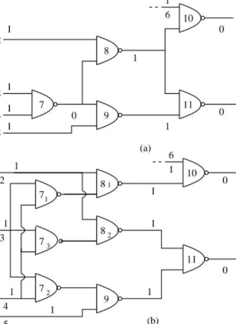
Let us consider the example in Figure 2(b) again. Back- trace from 10 and 11. Backtrace from 10 to 81 and 71, which stops at 6 because the corresponding paths are not included in the SPC circuit. It is found that a1/0 and b1/0 are detected by the test. Backtrace from 11 to 82 and 9, and to 73 and 72, respectively. It is clear that faults a2/0, b2/0, a3/0, and b3/0 are covered by the test. That is, the test pair {1, 2, 3, 4, 5} = {11, 11, 01, 01, 11} covers the rising transition path delay faults on paths {3-7-8-10, 3-7- 8-11, 3-7-9-11, 4-7-8-10, 4-7-8-11, 4-7-9-11}, where the first value of the test pair is the initial value and the second is the stable value.
The backward fault simulation process does not need to traverse some nodes in an SPC circuit when the faults re- lated to an input or a fanout branch at an input have been covered. This technique can further reduce fault simulation time and prune the SPC circuit effectively. As shown in Figure 9, the path delay faults related to lines a and b have been covered. Both lines are assigned a star label. The line c is also assigned a star label. Let d be assigned a star la- bel too. It is clear that e must be assigned a star label. Therefore, it is unnecessary to traverse the lines preceding to e, where faults corresponding to all predecessors of e have been covered for the backward fault simulation from g. This selective backtracing technique can further save enough time when the SPC circuit contains no untestable path delay faults. The SPC circuit pruning technique cor- responds to the fault dropping process of the conventional fault simulators.
VI. Fault Simulation for Robustly Testable Path Delay Faults
Robust test generation for path delay faults can still be completed by using a single stuck-at test generation tool and the ETGC circuit model. The only differences are that the logic system must be replaced by the 10-valued logic system, and the robustly sensitizable conditions of all off-path lines are different. The robustly sensitizable conditions as presented in Figure 10 are as follows:
• As for a falling transition at an input of an AND gate or NAND gate, its off-path inputs must be assigned value s1; let a rising transition at an input of an AND gate or NAND gate, its off-path inputs must be as- signed x1.
• All off-path inputs must be assigned x0 in order to propagate a falling transition on an input of an OR or NOR gate robustly; as for a rising transition on an input of an OR or NOR gate, its off-path inputs must be assigned s0.
• For a rising transition or a falling on an input of an XOR or a NXOR gate, its off-path inputs must be assigned s0 or s1.
A backward fault simulation procedure is proposed for ro- bustly testable paths in order to avoid the path set op- erations. This can greatly reduce CPU time to do fault simulation. This scheme does not need to keep a path set for each node in the SPC circuits, which can save a large amount of memory. The backward fault simulation proce- dure is still proposed based on the 4-valued logic simula- tion. It starts from the primary outputs or pseudo-primary outputs by using a selective backtracing procedure.
The robustly sensitizable conditions as presented in Fig- ure 10 are checked for all inputs at the output of a gate. Backtrace continues along the input if the conditions are met for it, otherwise, stop at that node. Continue the above process until reaching a primary input or a pseudo- primary input. All the detected path delay faults can be collected at the inputs of the SPC circuit. An input of the SPC circuit or only a branch at an input is pruned when all path delay faults related to the input in the SPC circuit have been covered. A gate in the SPC circuit can also be pruned if all its inputs have been pruned as presented in Figure 9. The computing complexity of the procedure in Figure 11 is O(vec · N ), where vec is the number of test vectors, and N is the size of the SPC circuit.
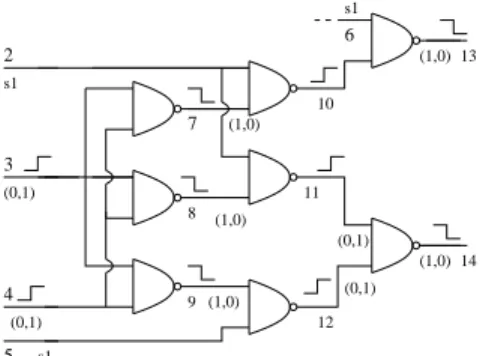
Experimental results are presented to demonstrate that the proposed backward fault simulation procedures obtain exact fault simulation results in Section 7. Theoretical proof of the exactness of the fault simulator is not pre- sented because of space limit. Figure 12 presents the logic simulation result for the robust test vector pair (2,3,4,5,6)
= (s1, s1, s1, s1, s1). The backward selective tracing iden- tifies the set of uncovered path delay faults. Let {p1, p2, p3, p4, p5, p6} = {3-7-10-13, 3-8-11-14, 3-9-12-14, 4-7-10-13, 4-8-11-14, 4-9-12-14}. The robust test vector pair detects rising transition path delay faults on all the above paths: {p1/r, p2/r, p3/r, p4/r, p5/r, p6/r}.
VII. Experimental Results
We have implemented the fault simulator called Fas- tExact for non-robustly and robustly testable path delay
Table 1: Testable Path Selection based on ZBDD [12] robust non-robust
Circuit paths CPU paths CPU
s298 343 0.03 364 0.04
s344 611 0.05 654 0.07
s349 611 0.05 656 0.08
s382 667 0.05 734 0.1
s386 413 0.04 414 0.09
s400 663 0.04 753 0.09
s420 738 2.59 738 0.13
s444 586 0.05 813 0.1
s510 729 0.07 738 0.1
s526 729 0.07 738 0.1
s641 1979 0.22 2270 0.35 s713 1184 0.24 4922 0.58
s820 980 0.21 984 0.18
s832 984 0.23 996 0.21
s838 2018 0.2 2018 0.2
s953 2302 0.18 2312 0.12 s1196 3581 0.72 3759 0.34 s1238 3589 0.83 3684 0.35 s1488 1875 0.38 1916 0.33 s1494 1882 0.38 1927 0.32 s1423 28696 10.88 45198 11.33 s5378 18656 3.45 21928 2.47 s9234 21389 57.01 59854 51.96 s13207 27603 10.45 476143 26.18 s35932 21783 30.59 58657 31.88 s38584 92239 62.81 334927 37.33
faults. As for non-robustly testable path delay faults, the fault simulator is completed on the SPC circuit based on the 3-valued (0, 1, and ×) logic simulation, where the SPC is constructed by the selected non-robustly testable paths [12]. As for the robustly testable path delay faults, the fault simulator is implemented based on the 4−valued logic simulation (s0 (0,0), s0 (1,0), s1 (0,1), s1 (1,1)) cor- responding to the 10-valued logic system, where the SPC is constructed by the robustly testable paths. The ro- bustly testable paths and non-robustly testable paths are obtained based on the ZBDD in [12]. Table 1 presents the number of robustly testable paths and non-robustly testable paths, and the CPU time (seconds) for ZBDD to acquire these testable paths. As shown in Table 1, ro- bustly testable paths and non-robustly testable paths are obtained for all circuits in very short CPU time.
The FastExact fault simulator is implemented by C lan- guage using a Blade2000 workstation. FastExact is run on the larger ISCAS89 circuits for the non-robust and robust test sets, where the deterministic test vector pairs are ob- tained by a stuck-at-test-based test generator [18]. The paths represents the number of non-robustly testable or robustly testable paths as shown in Table 2. In Table 2, init and fsim represent CPU time (seconds) to construct the SPC circuit and for the fault simulation, respectively. The parameter vec. represents the number of test vec- tors. FastExact obtains 100% fault coverage for all cir-
cuits. Table 2 presents fault simulation results of all non- robustly testable paths and robustly testable paths for all circuits except s15850 for non-robustly testable paths. Cir- cuit s15850 uses only a subset of the longest non-robustly testable path delay faults.
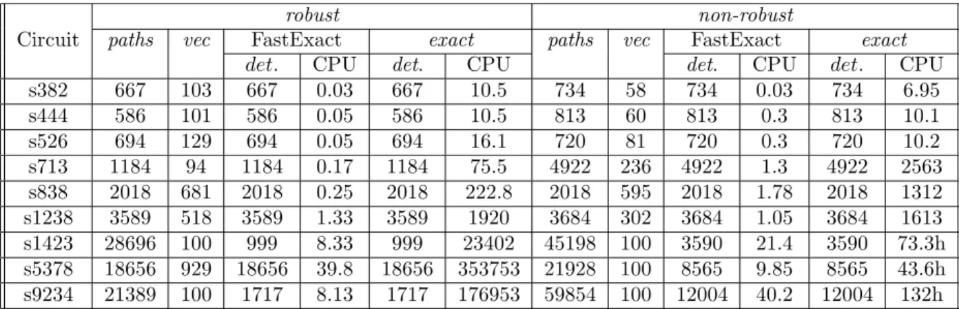
Table 3 presents comparison of the fault simulation re- sults with FastExact and the exact fault simulation results. The exact fault simulation checks all undetected path de- lay faults in the fault list one by one whenever there is a transition in the inputs of the circuit. It checks from the source node of a path to the sink node. A path delay fault is covered if all off-path lines are assigned sensitiza- tion values. In Table 3, parameters exact, FastExact, det., paths, and vec. represent the exact fault simulation re- sults, the proposed fault simulation results, the number of path delay faults detected by the test pair set, the number of path delay faults under consideration, and the number of test pairs. Parameter CPU represents the CPU time (seconds) only for the fault simulation, not including the time to construct the SPC circuit. It is found that for all circuits FastExact obtains exactly the same number of de- tected faults as that of the exact fault simulator. However, FastExact needs much less CPU time (seconds). The ex- act fault simulation avoids creating a separate SPC circuit, and instead it keeps the list of all the nodes on the path currently under evaluation and the sensitization values of their off-path lines. So the exact fault simulation requires less storage than our proposed method. However, it needs more CPU time to simulate all the undetected path de- lay faults one by one. Only 100 test pairs are checked for circuit s1423 because too much CPU time is required for exact fault simulation, so is circuit s9234. The experimen- tal results for random test pairs also prove the accuracy of our proposed fault simulator, which are not presented for space limit.
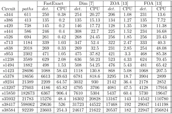
Table 4 presents comparison of the FastExact fault sim- ulator with the DIM [7], ZOA [13](the zero order) fault simulator and FOA (the first order) fault simulator in [13] using the deterministic robust test vectors generated by the SPC test generator [18]. It is found that the DIM fault simulator needs much more CPU time (seconds) than that of the FastExact fault simulator in all cases. However, the DIM fault simulator still includes some undetected faults in almost all cases. It also missed some detected faults in some cases. The ZOA [13] fault simulator obtains a pes- simistic fault coverages for all circuits in very short time. As for the FOA [13] fault simulator, it obtains pessimistic fault coverage estimation for all circuits in much more CPU time than FastExact. Only 1000 test pairs are used for cir- cuits s1423, s15850, and s38417 because the FOA and DIM fault simulators needs too much CPU time.
Table 5 compares the performance of the FastExact fault simulator with DIM [7], ZOA [13](the zero order fault simulator) and the FOA fault simulator in [13] with 1000 random test pairs. The DIM fault simulator overesti- mates fault coverage in almost all cases in much more CPU time than that of FastExact. The fault simulators ZOA and FOA underestimate fault coverage in almost all cases, while the FOA needs much more CPU time than that of FastExact and ZOA needs even less CPU time than that of FastExact in some cases.
robust non-robust
Circuit paths vec. FC cpu(s) paths vec. FC cpu(s)
init fsim init fsim
s13207 27603 2727 100 4.2 78.7 476143 2439 100 162 1238
s35932 21783 278 100 6.4 15.7 58657 69 100 18.2 9.97
s38417 598062 32348 100 585 20625 1138149 15658 100 1114 15471 s38584 92239 3484 100 18.3 282 334922 3842 100 188 1281 s15850 182673 7557 100 478 5813 121525 2417 100 447 3583
Table 2: Performance of the FastExact Path Delay Fault Simulator for Robust and Non-robust Tests
Table 3: Comparison with the Exact Fault Simulation Results
robust non-robust
Circuit paths vec FastExact exact paths vec FastExact exact
det. CPU det. CPU det. CPU det. CPU
s382 667 103 667 0.03 667 10.5 734 58 734 0.03 734 6.95
s444 586 101 586 0.05 586 10.5 813 60 813 0.3 813 10.1
s526 694 129 694 0.05 694 16.1 720 81 720 0.3 720 10.2
s713 1184 94 1184 0.17 1184 75.5 4922 236 4922 1.3 4922 2563
s838 2018 681 2018 0.25 2018 222.8 2018 595 2018 1.78 2018 1312 s1238 3589 518 3589 1.33 3589 1920 3684 302 3684 1.05 3684 1613 s1423 28696 100 999 8.33 999 23402 45198 100 3590 21.4 3590 73.3h s5378 18656 929 18656 39.8 18656 353753 21928 100 8565 9.85 8565 43.6h s9234 21389 100 1717 8.13 1717 176953 59854 100 12004 40.2 12004 132h
VIII. Conclusions
A fast and exact fault simulator called FastExact is pro- posed for path delay faults based on logic simulation and selected path sets. A new circuit called the SPC circuit is constructed by the non-robustly or robustly testable paths, which contains fanouts only at the inputs of the SPC circuit. A backward selective tracing scheme is run on the SPC circuit for non-robustly testable faults to pro- ceed only the active part based on logic simulation results of all nodes, where the logic simulation results are obtained on the original circuit. The backward selective tracing scheme does not need to store any fault list, therefore, does not need any extra memory. An effective fault dropping scheme is also adopted to prune the SPC circuit in the process of fault simulation. Experimental results confirm the accuracy of the proposed fault simulator. Experimen- tal results are presented to compare with several previous methods on CPU time and accuracy. In the future re- search, more efforts would be made to propose an effective procedure instead of ZBDD in [12] to select testable path delay faults.
References
[1] N. M. Abdulrazzaq and S. K. Gupta, “Path delay fault simulation for circuits with large numbers of paths for very large test sets,” in Proc. of 21th IEEE VLSI test Symposium, pp. 186-193, 2003.
[2] K. T. Cheng and H. C. Chen, “Classification and iden- tification of non-robust untestable path delay faults,”
IEEE Trans. on Computer-Aided Design, vol. 15, no. 8, Aug. 1996.
[3] K. Fuchs, F. Fink, and M. H. Schulz, “DYNAMITE: An efficient automatic test pattern generation system for path delay faults,” IEEE Trans. on Computer- Aided Design, vol. 10, no. 10, pp. 1323-1335, 1991. [4] F. Fink, K. Fuchs, and M. H. Schulz, “Robust and
non-robust path delay fault simulation by parallel processing of patterns,” IEEE Trans. on Computers, vol. 41, no. 12, pp. 1527-1536, 1992.
[5] M. A. Gharaybeh, M. L. Bushnell, and V. D. Agawal,
“The path-status graph with application to delay fault simulation,” IEEE Trans. on Computer-Aided Design, vol. 17, no. 4, pp. 324-332, 1998.
[6] K. Heragu, J. H. Patel, and V. D. Agrawal, “Improv- ing a non-enumerative method to estimate path de- lay fault fault coverage,” IEEE Trans. on Computer- Aided Design, vol. 16, no. 7, pp. 759-762, 1997. [7] D. Kagaris and S. Tragoudas, “On the non-
enumerative fault simulation problem,” IEEE Trans. on CAD, vol. 21, no. 9, pp. 1095-1101, 2002.
[8] B. Kapoor, “An efficient method for computing exact path delay fault coverage,” in Proc. of IEEE European Design and test Conference, pp. 516-520, 1995. [9] A. Krstic and K. T. Cheng, Delay Fault Testing for
VLSI Circuits, Kluwer Academic, 1998.
[10] H. K. Lee and D. S. Ha, “On the generation of test patterns for combinational circuits,” Technical Report12-93, Dept. of Electrical Eng., Virginia Poly- technic Institute and State University, 1993.
FastExact Dim [7] ZOA [13] FOA [13]
Circuit paths vec. det. CPU det. CPU det. CPU det. CPU
s349 611 95 611 0.05 606 1.9 321 0.12 446 2.1
s382 667 103 667 0.03 679 1.7 433 0.13 593 3.9
s386 413 118 413 0.03 413 1.15 407 0.15 413 0.95
s400 663 102 663 0.05 679 1.78 419 0.12 575 4.1
s420 738 244 738 0.05 738 5.68 453 0.33 570 3.62
s444 586 101 586 0.05 674 2 415 0.15 573 4.62
s510 729 218 729 0.1 737 3.95 464 0.37 687 6.52
s526 694 129 694 0.05 701 2.32 609 0.23 686 3.17
s641 1979 179 1979 0.62 1937 31.82 669 0.4 1708 10.58
s713 1184 94 1184 0.17 1224 10.7 553 0.25 1070 7.07
s832 984 242 984 0.15 991 5.27 967 0.73 979 8.65
s838 2018 681 2018 0.25 2019 81.8 1152 1.92 1521 44.33 s953 2302 395 2302 0.45 2313 29.5 1147 1.33 2061 55.98 s1196 3584 544 3584 1.38 3575 67.33 1648 2.28 3201 87.58 s1238 3589 518 3589 1.33 3543 62.08 1699 2.27 3199 87.28 s1494 1882 384 1882 0.55 1895 36.58 1526 2.05 1795 32.25 s1423 28696 1000 6244 84.4 6028 465.7 1311 5.13 4045 398 s5378 18656 929 18656 39.8 18696 2722 6166 17.0 10198 26201 s9234 21389 1549 21389 84.1 22501 7219 7195 49.2 12496 6782 s13207 27603 2796 27603 279 28105 26217 16248 132 18224 53250 s15850 182673 1000 27608 1081 28824 14387 10601 55.6 21888 211140 s35932 21783 166 21783 10.9 26422 10417 18905 24.1 20622 28546 s38417 598062 1000 64460 530 66836 58485 34664 162 53387 141231 s38584 92239 2788 92239 706 91553 42.7h 37371 465 62454 197.4h
Table 4: Comparison with the Previous Fault Simulators with the Deterministic Tests Generated by [18]
FastExact Dim [7] ZOA [13] FOA [13]
Circuit paths det. CPU det. CPU det. CPU det. CPU
s344 611 250 0.38 254 20.27 206 1.08 231 13.6
s386 413 135 0.2 135 15.13 134 1.27 135 7.72
s420 738 145 0.2 146 17.72 128 1.35 138 11.38
s444 586 246 0.4 308 22.7 225 1.52 234 16.68
s526 694 261 0.42 268 24.45 256 1.85 256 23.43
s713 1184 339 1.03 347 52.4 322 2.47 333 40.3
s838 2018 269 0.33 269 32.5 231 2.85 254 48.08
s953 2302 471 1.05 475 37.82 421 3.3 468 85.38
s1238 3589 629 2.08 636 50.23 523 4.33 624 70.45
s1494 1882 498 1.53 508 54.25 476 5.43 481 65.42
s1423 28696 1088 58.43 1118 130.8 868 5.08 1068 207.5 s5378 18656 6613 39.63 6781 818.6 3295 18.7 3904 2899 s9234 21389 2209 64.57 3032 930 2142 36.4 2178 2852 s13207 27603 4186 65.82 4795 3706 4081 47.5 4128 17916 s15850 182673 6367 906.4 7610 5304 5437 60.4 5730 19647 s35932 21783 15276 48.4 16302 20828 13167 143 14542 110780 s38417 598062 29636 526 31723 44522 17468 192 29047 141198 s38584 92239 23603 254.3 24617 21622 20537 182 22947 256824
Table 5: Comparison with the Previous Fault Simulators with 1000 Random Test Vectors
[11] S. Ohtake, K. Ohtani, and H. Fujiwara, “A method of test generation for path delay faults using stuck- at fault test generation algorithms,” in Proc. of IEEE/ACM DATE, pp. 310-315, 2003.
[12] S. Padmanaban and S. Tragoudas, “Efficient identi- fication of (critical) testable path delay faults using decision diagrams,” IEEE Trans. on Computer-Aided Design, vol. 24, no. 1, pp. 77-87, 2005.
[13] I. Pomeranz and S. M. Reddy, “An efficient non- enumerative method to estimate path delay fault coverage,” IEEE Trans. on Computer-Aided Design, vol. 13, no. 2, pp. 240-250, 1994.
[14] A. Saldanha, R. K. Brayton, and A. L. Sangiovanni- Vincentelli, “Equivalence of robust delay-fault and single stuck-at fault test generation,” in Proc. of ACM/IEEE DAC, pp. 173-176, 1992.
[15] J. Saxena and D. K. Pradhan, “A method to derive compact test sets for path delay faults in combina- tional circuits,” in Proc. of IEEE Int. Test Confer- ence, pp. 724-733, 1993.
[16] M. H. Schulz, F. Fink, and K. Fuchs, “Parallel pat- tern fault simulation of path delay faults,” in Proc. of ACM/IEEE DAC, June, pp. 357-363, 1989.
[17] Y. Wu and A. Ivanov, “Accelerated path delay fault simulation,” in Proc. of IEEE VLSI Test Symposium, pp. 1-6, 1992.
[18] D. Xiang, K. Li, H. Fujiwara, and J. Sun, “Generat- ing compact robust and non-robust tests for complete coverage of path delay faults based on stuck-at tests,” in 24th Proc. of IEEE Int. Conference on Computer Design, pp. 446-451, 2006.

![Table 1: Testable Path Selection based on ZBDD [12] robust non-robust](https://thumb-ap.123doks.com/thumbv2/123deta/5753755.27196/7.918.105.397.100.619/table-testable-path-selection-based-zbdd-robust-robust.webp)