79:1 (2017) 81–88 | www.jurnalteknologi.utm.my | eISSN 2180–3722 |
Jurnal
Teknologi Full Paper
TEST REGISTER INSERTION AT RTL BASED ON
REDUCED BIST
Norlina Paraman
a*, Chia Yee Ooi
b, Ahmad Zuri Sha’ameri
a, Hideo
Fujiwara
ca
Faculty of Electrical Engineering, Universiti Teknologi Malaysia,
81310 UTM Johor Bahru, Johor, Malaysia
b
Malaysia-Japan International Institute of Technology, Universiti
Teknologi Malaysia Kuala Lumpur, Jalan Sultan Yahya Petra, 54100
Kuala Lumpur, Malaysia
c
Faculty of Informatics, Osaka Gakuin University, Osaka 564-8511,
Japan
Article history Received 8 May 2016 Received in revised form
6 November 2016 Accepted 10 December 2016
*Corresponding author
[email protected]
Graphical abstract
R2 CLB1
CLB3 CLB2
R3
(a)
R2 CLB1
CLB3 CLB2
R3
(b) TPG TPG
PO RA
PI PI
Abstract
Built-in self-test (BIST) method has high area overhead and long test application time. In this paper, a new BIST method is proposed at register transfer level (RTL) as a design for testability (DFT) method to modify a given RTL circuit to a reduced BIST- able RTL circuit. First, we introduce modelling method called extended R-graph to represent the register connectivity of an RTL circuit. The original register in the RTL circuit is modified into multiple input signature registers (MISRs) as test register. The selection of MISR is performed by extended minimum feedback vertex set (MFVS) algorithm that identifies a set of vertices (representing test register) which breaks all the loops of extended R-graph with minimal cost when vertices are removed. It has been proven through simulation that the proposed BIST method has lower area overhead of 32.9% on average and achieves comparably high fault coverage compared to the previous method, concurrent BIST using ITC'99 benchmark circuits.
Keywords: Built in Self-Test (BIST), test register, register transfer level (RTL), multiple input signature register (MISR)
Abstrak
Kaedah ujian-sendiri terbina-dalam (BIST) mempunyai kawasan overhed yang tinggi dan penggunaan masa ujian yang panjang. Di dalam kertas ini, kaedah baru BIST dicadangkan di aras pindahan daftar (RTL) sebagai kaedah rekabentuk untuk pengujian (DFT) untuk mengubah litar RTL kepada litar RTL reduced BIST-able. Pertama, kami memperkenalkan pemodelan yang dinamakan R-graph lanjutan untuk mewakili penyambungan daftar di litar RTL. Daftar yang asal diubahsuai kepada daftar tandatangan berbilang input (MISR) sebagai daftar ujian. Pemilihan daftar sebagai MISR dilakukan oleh algoritma set verteks minimum yang mengenal pasti set vertex (mewakili daftar ujian) yang memutuskan semua gelung R-graph lanjutan dengan kos yang minimum apabila vertex disingkirkan. Ia telah dibuktikan melalui simulasi kaedah BIST yang dicadangkan mempunyai kawasan overhed yang lebih rendah sebanyak 32.9% secara purata dan setanding tinggi dari segi liputan kerosakan berbanding dengan kaedah yang terdahulu, BIST serentak, menggunakan penanda aras litar ITC’99.
Kata kunci: Ujian-sendiri terbina-dalam, daftar ujian, aras pindahan daftar, daftar tandatangan berbilang input,
© 2017 Penerbit UTM Press. All rights reserved
1.0 INTRODUCTION
With the advancement in semiconductor technology, the complexity of Very-Large-Scale Integration (VLSI) designs is growing and the cost of testing is increasing. The external test with time- consuming scan-in and scan-out of test data and expensive test equipment has become a bottleneck in testing due to limited input / output channels, bandwidth and speed of the external automated test equipment (ATE). The problems of ATE can be overcome by integration of built-in-self-test (BIST) technique in a circuit [1]. In this technique, test pattern generators (TPGs) are added to primary inputs (PIs) and response analysers (RAs) are added to primary outputs (POs). Thus, the circuit is enabled to generate test patterns internally and compact the output responses. However, adding these TPGs and RAs is not sufficient to achieve high fault coverage (even for single stuck-at faults) if the circuit contains loops in its structure. Therefore, several techniques BIST have been proposed [1].
Basically, selected registers in the circuit-under- test (CUT) are modified into test registers in order to improve the CUT’s connectivity. This is because test register is able to generate test patterns or compact test responses in the test mode. Test registers could be BILBO (built in logic block observer) [2], CBILBO (concurrent BILBO), MISR (multiple input signature register) and LFSR (linear feedback shift register). BILBO and MISR are able to generate test patterns and compact test responses [3]. However, BILBO needs different test sessions to generate test pattern and compact test responses separately while MISR can perform the two functions in the same test session. CBILBO also can generate test patterns and compact test responses in the same test session like MISR while LFSR can generate test patterns only.
Generally, BIST schemes are classified into test- per-scan and test-per-clock. In the test-per-scan scheme, the test registers generate test patterns and compact test responses in a few clock cycles based on scan-in and scan-out processes through scan path [4, 5, 6]. Test-per-scan scheme requires low area overhead. However, it has long test application time. In the test-per-clock scheme, the test registers generate test patterns and compact test responses in one clock cycle. The main advantage of this scheme is low test application time. However, test- per-clock requires higher hardware overhead than the test-per-scan scheme does.
BIST technique in the test-per-clock scheme [7, 8, 9, 10] can be classified into two categories. The first category requires simultaneous testing of all combinational blocks whereas the second category requires each module to be tested independently from the other modules. These two methods add TPG at all primary inputs and RA at all primary outputs.
Wunderlich tested all combinational blocks simultaneously [7]. The DFT method augments a given circuit with BILBO or CBILBO so that the circuit
becomes easily testable. Therefore, every loop of the circuit must contain one CBILBO or two BILBOs in order to operate both TPG and RA in the same test session. The advantage of this scheme is short test application time, since all combinational blocks are tested simultaneously. However, this scheme has high area overhead since several internal registers are modified to become BILBOs and CBILBOs.
In order to reduce hardware overhead in [7], Masuzawa proposed a BIST method based on hierarchical test where each combinational module is tested independently from other modules [8]. The DFT method for this approach is called single control testability. This scheme does not require to add extra registers but only adds extra combinational logics to augment a given data path so that it is easily testable. Hence, the area overhead is lower than that in approach [7]. The disadvantage of this scheme is long test application time because only a single combinational module is tested at a time.
Yamaguchi [9, 10] proposed a new testability called concurrent single control testability to remedy the disadvantage of test application time in [8]. They extended the concept of the testability by introducing concurrent testing so that multiple combinational modules can be tested concurrently at a time. This scheme has shorter test application time than that in approach [8] but suffer from area overhead.
Nicolici proposed a BIST method that extracted structural information from data path [11]. The same type modules are grouped in test compatibility classes. Each class has more than one LFSR that used as test patterns generator. More than one test sessions are required to test the whole circuit. Besides, an extra comparator is added to check the output responses. Therefore, they needs more area overhead on top of overhead incur by LFSR and MISR.
According to Nassar and Salama, they proposed a method with minimum area overhead and minimum number of test sessions [12]. The algorithm of register allocation and binding was introduced. By using this algorithm, CBILBO and BILBO are applied in the CUT with minimum number of test sessions. Extra multiplexers are added to provide interconnection between the modules. Based on the analysis result, the proposed algorithm used CBILBO, BILBO, MISR, TPG and multiplexers to make the CUT easily testable. As a results, it suffers from high area overhead. More than one test sessions are required depending on the CUT design and its characteristics.
In this paper, we propose a BIST technique that test all combinational blocks simultaneously using test-per-clock scheme. The simulation result is compared with the same approach that use test- per-clock scheme and not with the scan BIST because scan BIST requires long test application time. We classify the circuit into three categories based on BIST type and BIST insertion method to make the circuit BIST-able. They are called primitive BIST-able RTL circuit, concurrent BIST-able RTL circuit and
reduced BIST-able RTL circuit (the proposed BIST). There is no element of DFT augmented into primitive BIST-able RTL circuit. For concurrent BIST-able RTL circuit, its DFT method using approach in [7]. In [7], they obtained short test application time and high area overhead. We improve approach in [7] by keeping the advantage of short test application time and alleviating the disadvantage of area overhead. In order to reduce area overhead, we replace CBILBO with MISR for each loop because MISR also can generate test pattern and compact test response simultaneously, similar to CBILBO. The selected register as MISR as test register is determined such that the area overhead is minimum. We also get similarly high fault coverage to that of the approach in [7].
This paper is organized as follows. In Section 2, we present the classification of BIST-able RTL circuits whose all combinational blocks are tested simultaneously. In Section 3, we define the DFT method for reduced BIST-able RTL circuit. In Section 4, we present the simulation results and Section 5 for conclusion.
2.0 METHODOLOGY
In this section, we classify the RTL circuits into three categories and introduce DFT method.
2.1 Classification of BIST-able RTL Circuits
The RTL circuits are classified into three categories based on BIST type and BIST insertion method. They are called primitive BIST-able RTL circuit, concurrent BIST-able RTL circuit and reduced BIST-able RTL circuit. Each category uses LFSR as test pattern generator at PI while MISR as register analyser at PO. For primitive BIST-able RTL circuit, no internal register is modified into test register. For concurrent BIST-able RTL circuit, the original registers for each loop are augmented into CBILBO. For reduced BIST-able RTL circuit, the original circuit is augmented using our proposed DFT by ensuring at least a MISR or transparent MISR for each loop. MISR operates similarly to CBILBO to generate test pattern and compact test response simultaneously. To facilitate our discussion, we define the primitive BIST-able RTL circuit, concurrent BIST-able RTL circuit and reduced BIST-able RTL circuit as follows.
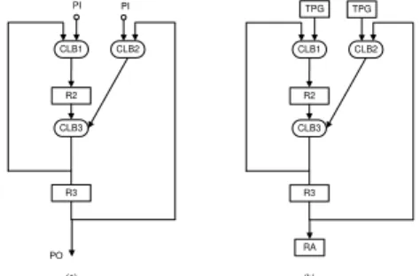
Definition 1 An RTL circuit is called primitive BIST-able if its primary inputs and primary outputs are modified into TPGs and RAs respectively.
Figure 1(a) shows the original circuit which is not self-testable. Figure 1(b) shows the primitive BIST-able RTL circuit. In order to make the circuit self-testable, we modify the PIs and POs into TPGs and RAs respectively as shown in Figure 1(b). During testing, the TPGs apply pseudorandom patterns to
combinational logic block (CLB) modules and the test responses of CLB modules are compressed by the register of PO which is modified into RA. Note that register R2 and R3 are not modified.
R2 CLB1
CLB3 CLB2
R3
(a)
R2 CLB1
CLB3 CLB2
R3
(b)
TPG TPG
PO RA
PI PI
Figure 1 (a) Original RTL circuit with two connected self- loops (b) Primitive BIST-able RTL circuit
Referring to this example, there is no DFT element inserted internally into the primitive BIST-able RTL circuit. This approach obtains low fault coverage due to the untestable caused by the loops in the circuit. Note that for every loop, the register is not modified into test register.
According to [7], they extend the primitive BIST- able circuit by inserting two BILBOs or one CBILBO in each loop to guarantee high fault coverage. It is known as concurrent BIST-able RTL circuit. In order to define concurrent BIST-able RTL circuit, the transparent CBILBO or transparent MISR is defined as follows.
Definition 2 A register, R is called transparent CBILBO or transparent MISR if it operates as wire in normal mode and operates as CBILBO or MISR in test mode.
Definition 3 An RTL circuit is concurrent BIST-able if the following conditions are satisfied:
i. Each loop has one CBILBO such that the CBILBO operates as TPG and RA simultaneously. If more than one register exist in a loop, just one register is modified into CBILBO and the rest of original registers are remained as unmodified register. ii. A transparent CBILBO is inserted
instead of several CBILBOs, if cost of area overhead of transparent CBILBO is lower than that of CBILBOs. iii. Primary inputs and primary outputs are modified into TPGs and RAs respectively.
Figure 2 shows two types of concurrent BIST-able RTL circuit. Figure 2(b) shows concurrent BIST-able with CBILBO for each loop and Figure 2(c) shows concurrent BIST-able with transparent CBILBO. Note that, in Figure 2(b), original register R2 is modified into CBILBO register (T2) and original register R3 is modified into CBILBO (T3). There is another solution to
make this original circuit self-testable. It also can be achieved by inserting just one transparent CBILBO (T4) at the sharing path of both loops as shown in Figure 2(c). Regarding the hardware cost, CBILBO is more expensive than BILBO and also inserting a transparent test register is more expensive than modifying an existing register with CBILBO.
T2 CLB1
CLB3 CLB2
T3
(c) R2 CLB1
CLB3 CLB2
R3 T4 transparent
CBILBO
CBILBO
CBILBO TPG TPG
RA
TPG TPG
RA
(b) R2
CLB1
CLB3 CLB2
R3
(a)
PI PI
PO
Figure 2 (a) Original circuit (b) Concurrent BIST-able RTL circuit with CBILBO register T2 and CBILBO register T3 in each loop (c) Concurrent BIST-able RTL circuit with one transparent CBILBO register T4
Similar to approach in [7], our approach replaces CBILBO with MISR to break each loop. In our approach, the MISR not only can compact test responses but also can generate test patterns simultaneously. Our method can get high fault coverage and low area overhead. We call it as reduced BIST-able RTL circuit. The reduced BIST-able RTL circuit is defined as follows.
Definition 4 An RTL circuit is reduced BIST-able if the following conditions are satisfied:
i. Each loop has one MISR such that the MISR operates as TPG and RA simultaneously. If more than one register exist in a loop, just one register is modified into MISR and the rest of original registers are remained as unmodified register.
ii. A transparent MISR is inserted instead of several MISRs, if cost of area overhead of transparent MISR is lower than that of the MISRs.
iii. Primary inputs and primary outputs are modified into TPGs and RAs respectively.
Figure 3 shows two types of reduced BIST-able RTL circuit. Figure 3(b) shows reduced BIST-able with a MISR (T5 and T6) for each loop and Figure 3(c) shows reduced BIST-able with a transparent MISR (T7). Note that original register R2 is modified into MISR register (T5) and original register R3 is modified into MISR (T6) in Figure 3(b). We also can insert only a transparent
MISR (T7) at the sharing path of both loops to make the circuit self-testable as shown in Figure 3(c). Regarding the cost, we choose the lower one between these two types based on the DFT method.
T5 CLB1
CLB3 CLB2
T6 MISR = TPG + RA
MISR = TPG + RA
(b)
(c) R2 CLB1
CLB3 CLB2
R3 T7
transparent MISR = (TPG
+ RA)
TPG TPG
RA
RA
TPG TPG
R2 CLB1
CLB3 CLB2
R3
(a) PI
PO PI
Figure 3 (a) Original RTL circuit (b) Reduced BIST-able RTL circuit with MISR register T5 and MISR register T6 in each loop (c) Reduced BIST-able RTL circuit with one transparent MISR register T7
Concurrent BIST-able RTL circuit and reduced BIST- able RTL circuit have different ways of breaking a loop in the circuit. DFT for concurrent BIST-able RTL circuit breaks a loop with CBILBO while DFT for reduced BIST-able RTL circuit breaks a loop with a MISR. The area cost of CBILBO is more expensive than the area cost of MISR. With the advantage of reduced area overhead by using a MISR, we call our approach reduced BIST-able RTL circuit. In addition, we also can get low test application time and comparable high fault coverage as in approach in [7].
2.2 DFT Method for Reduced BIST
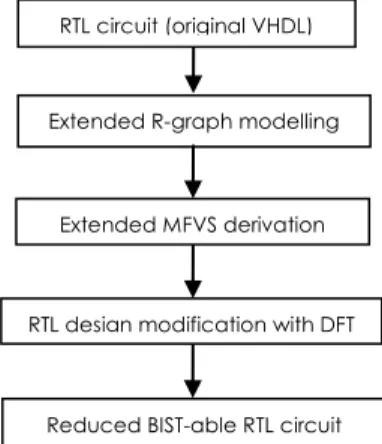
This section describes the DFT method that augments a given RTL into a reduced BIST-able RTL circuit. Figure 4 illustrates the DFT method for reduced BIST- able RTL circuit. Each benchmark circuit is written in VHDL that represents the RTL design. The RTL design uses a finite state machine with data path (FSM-D) model. Extended R-graph modelling is derived from VHDL. Next, extended MFVS is derived. The information of extended R-graph and extended MFVS are used to modify original RTL design with DFT. Then, reduced BIST-able RTL circuit is obtained.
Figure 4 DFT method for reduced BIST
2.2.1 Extended R-Graph
Similar to R-graph [13], extended R-graph is defined to represent the RTL circuit that contains the original register (node), test register (node) and connection between them (arc). The difference is extended R- graph has an extra vertex called dummy vertex, D. The purpose of dummy vertex is to represent the new hardware added as transparent test register. Extended R-graph is defined as follows.
Definition 5 An extended R-graph of an RTL is a directed graph G=(V,A,w) that has the following properties.
i. v∈V is a read node, write node or dummy node. If a read node and a write node correspond to the same variable, the same vertex represents them.
ii. (vi, vj)∈A denotes an arc if there exists a path from the read node vi
to the write node vj..
iii. (vi, vn)∈A denotes an arc if there exists a path from the read node vi
to the dummy vn.
iv. (vi, vm)∈A denotes an arc if there exists a path from the dummy vi to the dummy vm..
v. (vi, vs)∈A denotes an arc if there exists a path from the dummy vi to the write node vs.
vi. w:V→Z+ (the set of positive integers) defines the size of read, write node or dummy node corresponding to a vertex in V.
Read node is the input node (register) while write node is the output node (register). Properties i, ii, iii, iv and v explain the connection between vertices in extended R-graph. Arc is generated in several ways instead of between read node and write node. They are from dummy node to dummy node, read node to dummy node or write node to dummy node. Property vi describes the size of vertex.
Area Cost
Cost for each vertex that represents the corresponding register are included in the extended R-graph. Each vertex is added a cost except the primary input vertex and primary output vertex. One unit area is equal to the size of a NAND gate as used in Synopsys Design Vision. Cost, p(v) for each vertex of original register and dummy vertex are defined in the extended R-graph as follows.
i. Each cost of original vertex is 5wr. ii. Each cost of dummy vertex is12wd.
BILBO is used as MISR in the reduced BIST-able RTL circuit. The cost area added to augment an original vertex into MISR is 5. The cost area is 5 because it is the total area of additional logic of one AND gate, one NOR gate and one XOR gate as shown in Figure 5. The figure shows that cost area for AND gate, NOR gate and XOR gate are 1, 1 and 3, respectively such that the total cost area to insert 1-bit MISR is 5.
Figure 5 Area overhead for Figure 6 Area overhead for 1-bit register of MISR for 1-bit register of Transparent MISR
On the other hand, the cost area added to augment a dummy vertex into transparent test register is shown in Figure 6. It requires additional logic of one XOR gate, one multiplexer and one flip-flop to insert a new transparent MISR in the circuit. The area for multiplexer, XOR gate and flip-flop are 3, 3 and 6, respectively. Therefore, the total cost area to insert 1- bit transparent MISR is 12.
Figure 7 shows that each vertex except the primary input vertex and primary output vertex is assigned with a cost. The cost indicates the area overhead of the corresponding register when it is modified into a test register MISR or transparent MISR. R1 and R2 are original vertices while D1, D2 and D3 are dummy vertices. Thus, the cost of R1 and R2 are 5, and the cost of D1, D2 and D3 are 12.
PI1
R1
PI2 D1 D2 R2 PO
D3 12
12
5 5
12
Figure 7 An extended R-graph with cost area
Q
SETQ
CLR
D 3 Added flip-flop
mux 3 6
Q
SETQ
CLR
D 1
1 3
Original flip-flop
Extended R-graph modelling
Extended MFVS derivation
RTL design modification with DFT RTL circuit (original VHDL)
Reduced BIST-able RTL circuit
2.2.2 Extended MFVS
The algorithm of MFVS in [14] is used to identify the vertex that belong to minimum feedback vertex set (MFVS). At this paper, this algorithm is modified. The modified algorithm is called as extended MFVS. The extended MFVS is introduced in order to find a set of test registers such that the area overhead incurred (area cost) is minimum. Test register can be either MISR or transparent MISR. Note that test register MISR and transparent MISR are generated from original vertex and dummy vertex, respectively. Definition of extended MFVS is defined as follows.
Definition 6 An extended MFVS is a set of vertices V such that:
i. A vertex in the set of vertices, v∈V, breaks every loop.
ii. The summation cost of set of vertices that break the loops is minimized
∑ cost (v). v∈V
Two sets that break the loop are identified based on Definition 6. There are original vertex set and dummy vertex set. One of the sets is chosen as a test registers if that set has minimum total cost. Figure 7 shows the identification of vertex sets. Referring to Figure 7 two sets of MFVS is identified; original vertex set and dummy vertex are set. The MFVS of original vertex set is {R1, R2} and the MFVS of dummy vertex set is {D2}. Cost of each R1 and R2 is 5 and cost of D2 is 12. The total cost of original vertex set and dummy vertex set are 10 and 12, respectively. As a result, the original vertex set is selected as test register because the total cost of original vertex set is lower than that the total cost of dummy vertex set. Thus, R1 and R2 are modified into MISR to make the circuit testable. The test register is transparent MISR if dummy vertex set is selected as test register.
3.0 RESULTS AND DISCUSSION
3.1 Simulation Setup
RTL circuit is converted to its reduced BIST-able circuit using the method in Section 3. Next, reduced BIST- able RTL circuit is synthesized to its gate level netlist using Design Vision. The result of area is obtained by Design Vision. Another tool, fault simulation in TetraMax is used to obtain fault coverage. The pseudo random test pattern is generated using C++. The analysis and comparison of the results for each circuit is done in terms of area overhead, fault coverage and test application time to show the effectiveness of the proposed method compared to the previous method, concurrent BIST-able RTL circuit. The simulation has been conducted on ITC’99 benchmark [15] circuits. The characteristic of the benchmark circuits are shown in Table 1. Referring to
Table 1, FF represents the number of flip-flops while PI/PO represents the number of inputs/outputs of the circuit. The area column represents the area of the circuit where one unit of area is equal to the size of NAND gate.
Table 1 Characteristics of the benchmark circuits ITC’99 FF Area IO pins
PI PO
b01 5 90 4 2
b02 4 63 3 1
b03 30 422 6 4
b06 9 138 4 6
b09 28 391 3 1
b10 17 341 13 6
b11 31 788 9 6
b13 51 777 12 10 b14 215 10651 34 54
3.2 Simulation Results
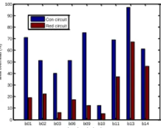
The effectiveness of reduced BIST method is measured in terms of fault coverage, area overhead and test application time. The model of single stuck- at-fault is considered during the simulation. The proposed method is compared with concurrent BIST- able RTL circuit [7] and primitive BIST-able RTL circuit. Figure 8 represents the percentage of the area overhead for concurrent BIST-able RTL circuit (con circuit) and reduced BIST-able circuit (red circuit). Since no DFT element is inserted into the primitive BIST-able RTL circuit except the TPGs and RAs, thus no area overhead is considered. One unit area is equal to the size of a NAND gate in the netlist. The area overhead for reduced BIST-able circuit is provided by the new gates added to the circuit during DFT insertion.
b01 b02 b03 b06 b09 b10 b11 b13 b14
0 10 20 30 40 50 60 70 80 90 100
benchmark circuits
area overhead (%)
Con circuit Red circuit
Figure 8 Area overhead for concurrent BIST-able RTL circuit and reduced BIST-able RTL circuit
It can be observed that all the benchmark circuits that have been augmented to reduced BIST-able RTL circuit have significantly lower area overhead compared to concurrent BIST-able RTL circuit. This is the main advantage of the proposed method. Area overhead of the proposed method is caused by the new gates added into the original register such that it becomes MISR, as test register. On the other hand, several new gates and another register are added to modify the original register to become CBILBO, as
0 10 20 30 40 50 60 70 80 90 100 0
20 40 60 80 100
clock cycles
fault coverage
con circuit red circuit pri circuit
0 50 100 150 200 250 300
0 20 40 60 80 100
clock cycles
fault coverage
con circuit red circuit pri circuit
0 50 100 150 200 250 300 350 400 450 500
0 20 40 60 80 100
clock cycles
fault coverage con circuit
red circuit pri circuit
0 50 100 150 200 250 300 350
0 20 40 60 80 100
clock cycles
fault coverage
con circuit red circuit pri circuit
0 1 2 3 4 5 6 7 8 9
x 104 0
20 40 60 80 100
clock cycles
fault coverage con circuit
red circuit pri circuit
0 1 2 3 4 5 6 7
x 104 0
20 40 60 80 100
clock cycles
fault coverage con circuit
red circuit pri circuit
0 1000 2000 3000 4000 5000 6000 7000 8000 9000
0 20 40 60 80 100
clock cycles
fault coverage
con circuit red circuit pri circuit
test register for concurrent BIST-able RTL circuit. Referring to circuit b02, only one register called stato that has 3 bits is modified into MISR and CBILBO. By modifying register stato into MISR and CBILBO, the area overhead incurs about 22% and 51%, respectively. In addition, the original register is modified into MISR at RTL such that the area overhead becomes low.
Next, the measurement in terms of fault coverage is shown. The graphs of fault coverage versus clock cycles for primitive BIST-able RTL circuit, concurrent BIST-able RTL circuit and reduced BIST-able circuit are shown in Figure 9 – Figure 17. The clock cycles are determined first. Next, the fault coverage is measured within the pre-determined clock cycles. The proposed method shows that the fault coverage is slightly lower than that of concurrent BIST-able RTL circuit for all the circuits. Since the test patterns generated by MISR for a combinational block partly depend on the test responses from the preceding combinational block, some of the random test patterns cannot be generated. Because there are not many useful random test patterns missed by the MISR, the fault coverage of our method is just slightly lower than that of concurrent BIST-able RTL circuit.
Figure 9 shows the fault coverage for circuit b01. The fault coverage for reduced BIST-able circuit and concurrent BIST-able RTL circuit are 15% and 20%, respectively in 20 clock cycles. After the clock cycles are up to 60, the fault coverage of our method increases to 83% compared to 88% for concurrent BIST-able RTL circuit. For circuit b09 in Figure 13, reduced BIST-able RTL circuit method obtains 82% while concurrent BIST-able RTL circuit achieves 86% after 7000 clock cycles. Circuit b09 needs more clock cycle of applying random test patterns in order to achieve the satisfactory fault coverage because the size of circuit b09 is bigger compared to circuit b01. This is supported by the results for other bigger circuits such as b10, b11, b13, b14 which need more than 1000 test patterns in order to achieve high fault coverage.
For circuit b11, b13 and b14, they need more than 50,000 test patterns to achieve high fault coverage. In these cases, MISR has 10 bits instead of 3 bits such that long sequences of test pattern are applied to detect a fault on circuit, thus, this increases the number of test patterns needed in the simulation.
Figure 9 Fault coverage for circuit b01
Figure 10 Fault coverage for circuit b02
Figure 11 Fault coverage circuit b03
Figure 12 Fault coverage for circuit b06
Figure 13 Fault coverage for circuit b09
Figure 14 Fault coverage for circuit b10
Figure 15 Fault coverage for circuit b11
0 0.2 0.4 0.6 0.8 1 1.2 1.4 1.6 1.8 2 x 10⁵ 0
20 40 60 80 100
clock cycles
fault coverage con circuit
red circuit pri circuit
0 2 4 6 8 10 12
x 104 0
10 20 30 40 50 60 70 80
clock cycles
fault coverage
con circuit red circuit pri circuit
Figure 16 Fault coverage for circuit b13
Figure 17 Fault coverage for circuit b14
4.0 CONCLUSION
A new BIST technique for RTL circuits has been introduced in this paper. A given RTL circuit is augmented by our DFT method is called reduced BIST-able RTL circuit. The DFT method modifies the original registers into MISR or transparent MISR to make the circuit easily testable. The proposed BIST method has lower area overhead by about 32.9% and achieves comparably high fault coverage compared to the previous method, concurrent BIST using ITC'99 benchmark circuits.
Acknowledgement
This research is fully supported by encouragement grant, Q.J130000.2623.11J03 PY/2014/03734. The authors fully acknowledged Universiti Teknologi Malaysia for the approved fund which makes this important research viable and effective.
References
[1] L. T. Wang, C. W. Wu and X. Wen. 2006. VLSI Test Principles and Architectures: Design for Testability. Burlington, MA: Morgan Kaufmann.
[2] B. Koenemann, J. Mucha and G. Zwiehoff. 1979. Built-in Logic Block Observation Techniques. IEEE Test Conference. 37- 41.
[3] Bin Zhou, Li-yi Xiao, Yi-Zheng Ye and Xin-Chun Wu. 2011. Optimization of Test Power and Data Volume in BIST Scheme Based on Scan Slice Overlapping. Journal of Electronic Testing: Theory and Applications. 43-56.
[4] Y. Sato, H. Yamaguchi, M. Matsuzono and S.Kajihara. 2011. Multi-Cycle Test with Partial Observation on Scan-Based BIST Structure. Asian Test Symposium. 54-59.
[5] S. Lei, Z. Wang, Z. Liu and F. Liang. 2010. A Unified Solution to Reduce Test Power for Test-Per-Scan Schemes. IEICE Electronics Express. 1364-1369.
[6] Ming-Jing, Jia-Guang Sun and H.Fujiwara. 2005. Improving Test Effectiveness of Scan-Based BIST by Scan Chain Partitioning. IEEE Transactions on Computer-Aided Design of Integrated Circuits and System. 916-927.
[7] A. P. Stroele and H. J. Wunderlich. 1998. Hardware-Optimal Test Register Insertion. IEEE Trans. on Computer-Aided Design of Integrated Circuits and Systems. 531-539. [8] T. Masuzawa, M. Idutsu, H. Wada and H. Fujiwara. 2000.
Single-Control Testability of RTL Data Paths for BIST. Proceeding 9th Asian Test Symposium. 210-215.
[9] K. Yamaguchi, H. Wada, T. Masuzawa and H. Fujiwara. 2001. A BIST Method Based on Concurrent Single-Control Testability of RTL Data Paths for BIST. Proceeding 10th Asian Test Symposium. 313-318.
[10] Kenichi Yamaghuci, Michiko Inoue and Hideo Fujiwara. 2007. Test-Per-Clock BIST with Low Overhead. Wiley Periodicals, Inc. Electronics and Communications in Japan Pt 2. 47-58.
[11] Nicola Nicolici. 2000. Power Minimisation Techniques for Testing Low Power VLSI Circuits. Ph.D. Thesis. University of Southampton.
[12] Nassar, D. A and Salama, A. E. 2002. A Heuristic DSP BIST Insertion Algorithm with Minimum Area Overhead. IEEE International Symposium on Circuits and Systems. 585-588. [13] Norlina Paraman, Chia Yee Ooi, Ahmad Zuri Sha'ameri and
Hideo Fujiwara. 2011. Built-in Self-Test for Functional Register-Transfer Level using Assignment Decision Diagram. IEEE Twelth Workshop on RTL and High Level Testing. 9-15. [14] Chakradhar, S. T., Balakrishnan, A. and Agrawal, V. D. 1994.
An Exact Algorithm for Selecting Partial Scan Flip-Flops. Proceeding of 31st ACM/IEEE Design Automation Conference. 81-86.
[15] http://www.cerc.utexas.edu/itc99 benchmarks/bench.html accessed 2015.